

Datasheet ALD500RAU-20SEI, ALD500RAU-20SE, ALD500RAU-20QEI, ALD500RAU-20QE, ALD500RAU-20PEI Datasheet (Advanced Linear Devices Inc)
...Page 1

ADVANCED
LINEAR
DEVICES, INC.
ALD500RAU/ALD500RA/ALD500R
PRECISION INTEGRATING ANALOG PROCESSOR
WITH PRECISION VOLTAGE REFERENCE
APPLICATIONS
• 4 1/2 digits to 5 1/2 digits plus sign measurements
• Precision analog signal processor
• Precision sensor interface
• High accuracy DC measurement functions
• Portable battery operated instruments
• Computer peripheral
• PCMCIA
FEATURES
• Resolution up to 18 bits plus sign bit and over-range bit
• Accuracy independent of input source impedances
• Accurate on-chip voltage reference
• Tempco as low as 10 ppm/°C guaranteed
• Chip select - power down mode
• High input impedance of 10
12
Ω
• Inherently filters and integrates any external noise spikes
• Differential analog input
• Wide bipolar analog input voltage range ±3.5V
• Automatic zero offset compensation
• Low linearity error - as low as 0.001% typical
• Fast zero-crossing comparator - 1µs
• Low power dissipation - 6mW typical
• Automatic internal polarity detection
• Low input current - 2pA typical
• Optional digital control from a microcontroller, an ASIC, or
a dedicated digital circuit
• Flexible conversion speed vs. resolution trade-off
BENEFITS
• Low cost, simple functionality
• Wide dynamic signal range
• Very high noise immunity
• Automatic compensation and cancellation
of error sources
• Easy to use to acquire bipolar signals
• Up to 19 bit (18 bit + sign bit) single conversion
or 21 bit (20 bit + sign bit) multiple conversion
and noise performance
• Inherently linear and stable with temperature
and component variations
PIN CONFIGURATION
ALD500R
I
1
B
C
2
INT
-
3
V
4
C
AZ
5
B
UF
6
AGND
-
7
C
REF
+
8
C
REF
9
N/C
10
N/C
QE, PE, SE PACKAGE
* N/C pin is connected internally. Connect to V
20
C
S
+
19
V
DGND
18
17
C
OUT
16
B
15
A
+
14
V
IN
-
V
13
IN
+
12
V
REF
-
11
V
REF
-
.
Ordering Information
Resolution Endpoint Voltage Reference Package Type Operating
16 bit 0.015% 0.5% 50ppm/C ALD500R-50PE ALD500R-50SE ALD500R-50QE 0°C to 70°C
17 bit 0.01% 0.3% 20ppm/C ALD500RA-20PE ALD500RA-20SE ALD500RA-20QE 0°C to 70°C
18 bit 0.005% ALD500RAU-20PE ALD500RAU-20SE ALD500RAU-20QE
17 bit 0.01% 0.2% 10ppm/C ALD500RA-10PE ALD500RA-10SE ALD500RA-10QE 0°C to 70°C
18 bit 0.005% ALD500RAU-10PE ALD500RAU-10SE ALD500RAU-10QE
17 bit 0.01% 0.3% 20ppm/C ALD500RA-20PEI ALD500RA-20SEI ALD500RA-20QEI -40°C to +85°C
18 bit 0.005% ALD500RAU-20PEI ALD500RAU-20SEI ALD500RAU-20QEI
18 bit 0.005% 0.3% 20ppm/C ALD500RAU-20DE -55°C to +125°C
Linearity Accuracy/Tempco Temperature
20L PDIP 20L SOIC 20L QSOP 20LCDIP
* Contact factory for customized voltage reference voltage levels, accuracy and tempco specifications.
Rev. 1.01 © 1999 Advanced Linear Devices, Inc., 415 Tasman Drive, Sunnyvale, California 94089-1706 Tel: (408) 747-1155, Fax: (408) 747-1286
http://www.aldinc.com
Page 2
R
= 100KΩ
REF
CB = 0.1µF
+
V
(14)
AGND
(6)
V
(13)
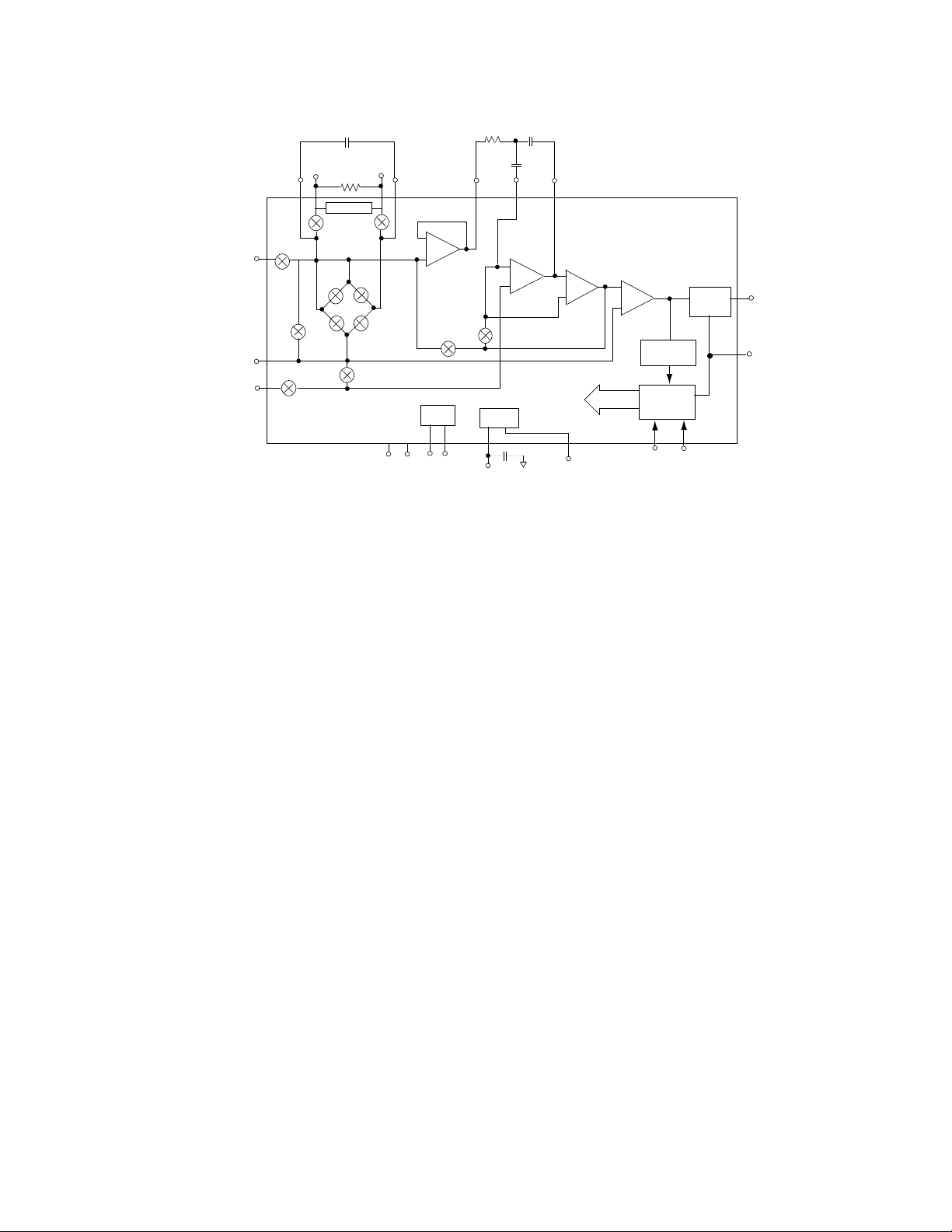
FIGURE 1. ALD500R Functional Block Diagram
C
N/C
SW
BUF
R
INT
INT
C
AZ
(5)
Integrator
+
AZ
Bias
C
B
I
B
(1)
C
INT
C
AZ
(2)
(4)
Comp1
Analog
Switch
Control
Signals
C
(20)
+
-
S
-
Comp2
+
Polarity
Detection
Phase
Decoding
Logic
A
B
(16)(15)
Control Logic
Level
Shift
C
OUT
(17)
DGND
(18)
C
REF
-
R
REF
REF
INT
SWRSW
-
SW
R
+
R
V
REF
(11)
R
+
R
-
SW
R
SW
G
SS
(3) (19) (10) (9)
-
C
REF
(7)
-
Buffer
+
SW
S
REF
Control
N/CVDDV
+
V
REF
(12)
+
C
REF
(8)
SW
IN
IN
SW
SW
Az
SW
SW
IN
-
IN
GENERAL DESCRIPTION
The ALD500RAU/ALD500RA/ALD500R are integrating
dual slope analog processors, designed to operate on ±5V
power supplies for building precision analog-to-digital
converters. The ALD500RAU/ALD500RA/ALD500R
feature specifications suitable for 18 bit/17 bit/16 bit
resolution conversion, respectively. Together with three
capacitors, two resistors, and a digital controller, a precision
Analog to Digital converter with auto zero can be
implemented. The digital controller can be implemented
by an external microcontroller, under either hardware
(fixed logic) or software control. For ultra high resolution
applications, up to 23 bit conversion can be implemented
with an appropriate digital controller and software.
The ALD500R series of analog processors accept
differential inputs and the external digital controller first
counts the number of pulses at a fixed clock rate that a
capacitor requires to integrate against an unknown analog
input voltage, then counts the number of pulses required
to deintegrate the capacitor against a known internal
reference voltage. This unknown analog voltage can then
be converted by the microcontroller to a digital word, which
is translated into a high resolution number, representing
an accurate reading. This reading, when ratioed against
the reference voltage, yields an accurate, absolute voltage
measurement reading.
The ALD500R analog processors consist of on-chip digital
control circuitry to accept control inputs, integrating buffer
amplifiers, analog switches, and voltage comparators and
a highly accurate, ultra-stable voltage reference. It
functions in four operating modes, or phases, namely auto
zero, integrate, deintegrate, and integrator zero phases.
At the end of a conversion, the comparator output goes
from high to low when the integrator crosses zero during
deintegration. ALD500R analog processors also provide
direct logic interface to CMOS logic families.
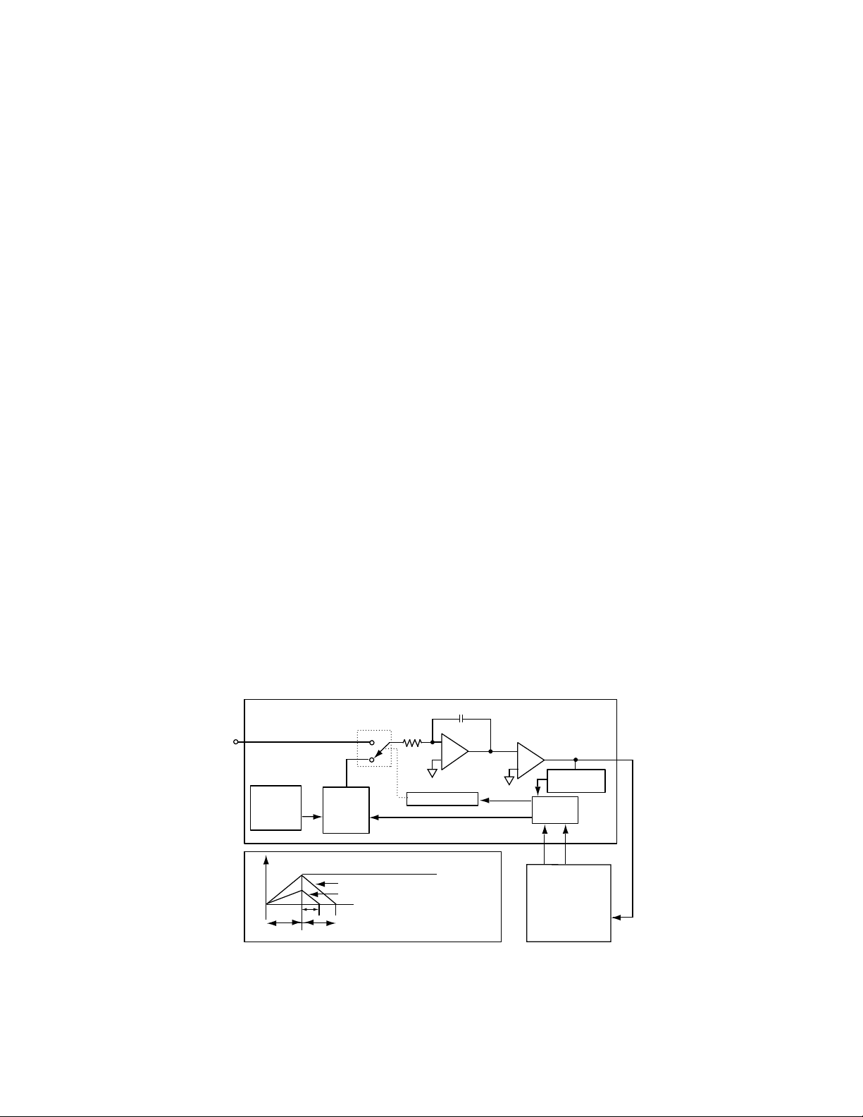
GENERAL THEORY OF OPERATION
Dual-Slope Conversion Principles of Operation
The basic principle of dual-slope integrating analog to digital
converter is simple and straightforward. A capacitor, C
charged with the integrator from a starting voltage, V
INT
, for a
X
, is
fixed period of time at a rate determined by the value of an
unknown input voltage, which is the subject of measurement.
Then the capacitor is discharged at a fixed rate, based on an
external reference voltage, back to V
where the discharge
X
time, or deintegration time, is measured precisely. Both the
integration time and deintegration time are measured by a
digital counter controlled by a crystal oscillator. It can be
demonstrated that the unknown input voltage is determined
by the ratio of the deintegration time and integration time, and
is directly proportional to the magnitude of the external reference
voltage.
The major advantages of a dual-slope converter are:
a. Accuracy is not dependent on absolute values of
integration time t
and deintegration time t
INT
DINT
, but is
dependent on their relative ratios. Long-term clock frequency
variations will not affect the accuracy. A standard crystal
controlled clock running digital counters is adequate to generate
very high accuracies.
b. Accuracy is not dependent on the absolute values of
R
INT and CINT
, as long as the component values do not vary
through a conversion cycle, which typically lasts less than 1
second.
c. Offset voltage values of the analog components, such
as VX, are cancelled out and do not affect accuracy.
d. Accuracy of the system depends mainly on the accuracy
and the stability of the voltage reference value.
2 Advanced Linear Devices ALD500RAU/ALD500RA/ALD500R
Page 3
e. Very high resolution, high accuracy measurements
can be achieved simply and at very low cost.
An inherent benefit of the dual slope converter system is noise
immunity. The input noise spikes are integrated (averaged to
near zero) during the integration periods. Integrating ADCs
are immune to the large conversion errors that plague
successive approximation converters and other high resolution
converters and perform very well in high-noise environments.
The slow conversion speed of the integrating converter provides
inherent noise rejection with at least a 20dB/decade attenuation
rate. Interference signals with frequencies at integral multiples
of the integration period are, theoretically, completely removed.
Integrating converters often establish the integration period to
reject 50/60Hz line frequency interference signals.
The relationship of the integrate and deintegrate (charge
and discharge) of the integrating capacitor values are
shown below:
.
V
INT
= VX - (V
IN
t
/ R
. C
INT
INT
INT
)
(integrate cycle) (1)
.
= V
INT
- (V
V
X
REF
t
DINT
/ R
INT
.
C
)
INT
(deintegrate cycle) (2)
Combining equations 1 and 2 results in:
V
/ V
REF
= -t
IN
DINT
/ t
INT
(3)
V
= Reference Voltage
REF
C
= Integrating Capacitor value
INT
R
= Integrating Resistor value
INT
Actual data conversion is accomplished in two phases: Input
Signal Integration Phase and Reference Voltage Deintegration
Phase.
The integrator output is initialized to 0V prior to the start of
Input Signal Integration Phase. During Input Signal Integration
reference voltage is integrated
Phase, internal analog switches connect V
to the buffer
IN
input where it is maintained for a fixed integration time period
(t
). This fixed integration period is generally determined by
INT
a digital counter controlled by a crystal oscillator. The
application of V
a rate determined by V
polarity of V
causes the integrator output to depart 0V at
IN
.
IN
and a direction determined by the
IN
The Reference Voltage Deintegration Phase is initiated
immediately after t
, within 1 clock cycle. During
INT
ReferenceVoltage Deintegration Phase, internal analog
switches connect a reference voltage having a polarity opposite
that of V
to the integrator input. Simultaneously the same
IN
digital counter controlled by the same crystal oscillator used
above is used to start counting clock pulses. The Reference
Voltage Deintegration Phase is maintained until the comparator
output inside the dual slope analog processor changes state,
indicating the integrator has returned to 0V. At that point the
digital counter is stopped. The Deintegration time period
), as measured by the digital counter, is directly
(t
DINT
proportional to the magnitude of the applied input voltage.
where:
V
x
V
INT
V
IN
t
INT
t
DINT
= An offset voltage used as starting voltage
= Voltage change across C
during t
(equal in magnitude)
DINT
during t
INT
INT
and
= Average, or an integrated, value of input voltage
to be measured during t
(Constant VIN)
INT
= Fixed time period over which unknown voltage is
integrated
= Unknown time period over which a known
R
INT
ANALOG
INPUT
(V
)
IN
VOLTAGE
REFERENCE
OUTPUT
INTEGRATOR
t
INT
t
DINT
t
DINT
SWITCHES
S1
REF
V
IN ≈ VFULL SCALE
V
IN ≈ 1/2VFULL SCALE
V
≈
0
x
After the digital counter value has been read, the digital
counter, the integrator, and the auto zero capacitor are all
reset to zero through an Integrator Zero Phase and an Auto
Zero Phase so that the next conversion can begin again. In
practice, this process is usually automated so that analog-todigital conversion is continuously updated. The digital control
is handled by a microprocessor or a dedicated logic controller.
The output, in the form of a binary serial word, is read by a
microprocessor or a display adapter when desired.
C
INT
INTEGRATOR
-
+
SWITCH DRIVER
POLARITY CONTROL
V
INT
= 4.1V MAX
V
INT
PHASE
CONTROL
COMPARATOR
-
+
POLARITY
DETECTION
CONTROL
LOGIC
AB
MICROCONTROLLER
(CONTROL LOGIC
+ COUNTER)
C
OUT
Figure 2. Basic Dual-Slope Converter
ALD500RAU/ALD500RA/ALD500R Advanced Linear Devices 3
Page 4
ABSOLUTE MAXIMUM RATINGS
Supply voltage, V
Differential input voltage range -0.3V to V+ +0.3V
Power dissipation 600 mW
Operating temperature range PE, SE package 0°C to +70°C
Operating temperature range QE package -55°C to +125°C
Storage temperature range -65°C to +150°C
Lead temperature, 10 seconds +260°C
+
13.2V
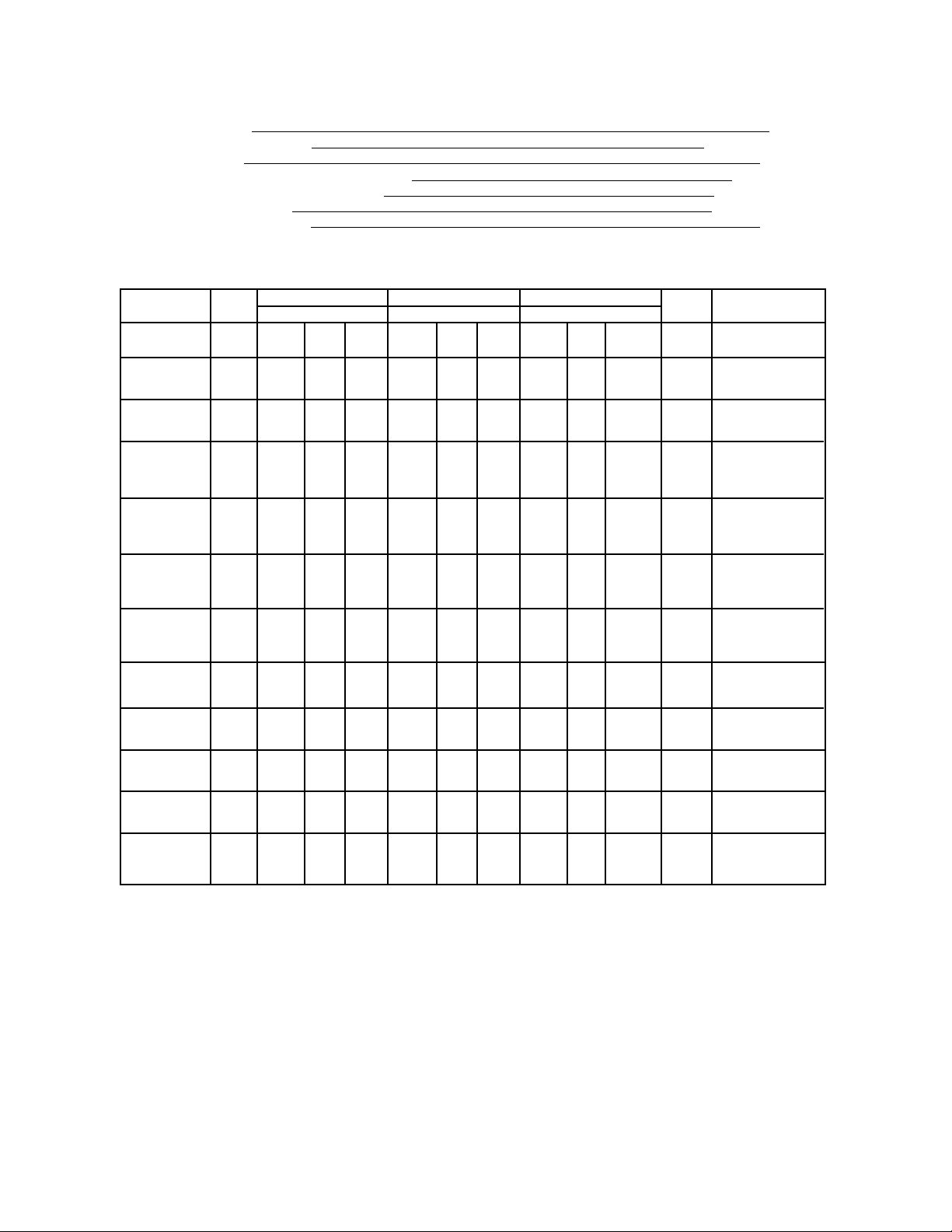
OPERATING ELECTRICAL CHARACTERISTICS
T
= 25°C V
A
+
= +5V V- = -5V (V supply ± 5V) unless otherwise specified; CAZ = C
REF
= 0.47µf
500RAU 500RA 500R
Parameter Symbol Min Typ Max Min Typ Max Min Typ Max Unit Test Conditions
Resolution 15 30 60 µV Notes 1, 7
Zero-Scale Z
Error 0.003 0.005 0.008 %
End Point E
Linearity 0.007 0.015 0.020 0°C to +70°C
Best Case N
Straight Line
SE
NL
L
0.0025 0.003 0.005 % 0°C to 70°C
0.001 0.005 0.003 0.010 0.005 0.015 % Notes 1, 2
0.0025 0.003 0.005 0.003 0.008 % Notes 1, 2
Linearity 0.004 0.008 0.015 0°C to +70°C
Zero-Scale TC
Temperature
ZS
0.3 0.6 0.3 0.7 0.3 0.7 µV/°C0°C to +70°C
Coefficient 0.15 0.3 0.15 0.35 0.15 0.35 ppm/°C Notes 1, 7
Full-Scale S
Symmetry Error
YE
0.005 0.008 0.01 % 0°C to 70°C
(Rollover Error) 0.008 0.010 0.012 %
Full-Scale TC
Temperature Note 7
FS
1.3 1.3 1.3 ppm/°C0°C to +70°C
Coefficient
Input I
Current
IN
222pAV
= 0V
IN
Common-Mode CMVR V
Voltage Range
Integrator V
Output Swing
INT
Analog Input VINV
Signal Range
Voltage V
Reference
REF
+1.5
SS
V
+0.9
SS
+1.5
SS
V
+1
SS
V
-1.5 VSS+1.5
DD
V
-0.9 VSS+0.9
DD
V
-1.5 VSS+1.5
DD
VDD-1 V
+1 V
SS
V
V
-1.5
-0.9
-1.5
+1.5
SS
V
+0.9
SS
V
+1.5
SS
V
-1
+ 1
SS
DD
V
DD
V
DD
DD
V
DD
V
DD
V
DD
V
V
-1.5
V
-0.9
V AGND = 0V
-1.5
V
-1
DD
Range
4 Advanced Linear Devices ALD500RAU/ALD500RA/ALD500R
Page 5

DC & AC ELECTRICAL CHARACTERISTICS
= 25°C V supply = ±5.0V unless otherwise specified; CAZ = C
T
A
500RAU 500RA 500R
Parameter Symbol Min Typ Max Min Typ Max Min Typ Max Unit Test Conditions
Supply Current I
Power Dissipation P
Positive Supply Range V
S
D
4.5 5.5 4.5 5.5 4.5 5.5 V Note 4
+S
0.6 1.0 0.6 1.0 0.6 1.0 mA V+ = 5V , A =1,B=1
10 10 10 mW V supply= ±5V
REF
= 0.47µf
Negative Supply Range V
Comparator Logic 1, V
Output High
Comparator Logic 0, V
Output Low
Logic 1, Input High V
Voltage
Logic 0, Input Low V
Voltage
Logic Input Current I
Comparator Delay t
1.8432 MHz Clock
A INPUT
B INPUT
C
C
START
CONVERSION
CYCLE
OUT
OUT
Positive Input Signal
Negative Input Signal
-4.5 -5.5 -4.5 -5.5 -4.5 -5.5 V Note 4
-S
OH
44 4VI
OL
3.5 3.5 3.5 V
IH
IL
L
0.01 0.01 0.01 µA
D
Figure 3. ALD500R TIMING DIAGRAM
~
66.667 msec.
~
~
~
NOT VALID
NOT VALID
Auto Zero
Phase
Clock data in
as needed.
0.5416 µs
START DEINTEGRATION CYCLE
123,093
Clock Pulses
~
~
or clock data out
of counters within the
the microcontroller
or fixed logic controller,
START INTEGRATION CYCLE
SOURCE
0.4 0.4 0.4 V I
SINK
111V
111µsec Note 5
1 Conversion Cycle
123,093
Clock Pulses
~
~
66.667 msec.
~
~
Input Signal
Integration
Phase
~
~
Reference
Voltage
Deintegration
~
~
~
~
~
~
Integrator Zero
Phase
Auto Zero
Phase
Phase
Fixed number
of clock pulses
by design.
Variable
number of
clock pulses.
At VIN MAX,
max. number of
clock pulses
~
= 246,185
Fixed period of
approx.1 msec.
Stop counter upon
detection of comparator
output going from high
to low state.
START INTEGRATOR ZERO CYCLE
REPEAT
CONVERSION
CYCLE
= 400µA
= 1.1mA
ALD500RAU/ALD500RA/ALD500R Advanced Linear Devices 5
Page 6

DC ELECTRICAL CHARACTERISTICS
= 25°C V supply = +5.0V unless otherwise specified; CAZ = C
T
A
Parameter Symbol 500RAU-10 500RAU-20 500RAU-50 Unit Test Conditions
500RA-10 500RA-20 500RA-50
Min Typ Max Min Typ Max Min Typ Max
Voltage Reference V
Supply Voltage V
Rejection Ratio
R
RSR
0.998 1.000 1.002 0.997 1.000 1.003 0.995 1.000 1.005 V
95 95 95 dB
REF
= 0.47µf, R
500R-50
= 100KΩ (1% metal film)
REF
Temperature V
Coefficient
Long Term Drift ∆V
Warm Up Time 10 10 10 min. Note 7
Positive Supply V+ 4.5 5.5 4.5 5.5 4.5 5.5 V
Operating Voltage Range
Negative Supply V- -5.5 -4.5 -5.5 -4.5 -5.5 -4.5 V
Operating Voltage Range
Power Down Supply I
Current
NOTES:
1. Integrate time ≥ 66 msec., Auto Zero time ≥ 66 msec., V
Resolution = V
2. End point linearity at ±1/4, ±1/2, ±3/4 Full Scale after Full Scale adjustment.
3. Rollover Error also depends on C
4. Contact factory for other power supply operating voltage ranges, including Vsupply = ±3V or Vsupply = ±2.5V.
5. Recommended selection of clock periods of one of the following:
t clk = 0.27µsec, 0.54µsec, or 1.09µsec
which corresponds to clock frequencies of 3.6864 MHz, 1.8432 MHz, 0.9216 MHz respectively.
6. R
REF
7. Sample tested parameter.
INT
is 100K Ω 1% metal film, 50 ppm/C.
RTC
/ -0.08 -0.08 -0.08 ppm/ Note 7
REF
∆t 1000hrs
PD
/integrate time/clock period
, C
INT
REF
3 10 7 20 15 50 ppm/C°
25 25 25 µA Note 7
= 4V, VIN = 2.0V Full Scale
INT
, C
characteristics.
AZ
~
6 Advanced Linear Devices ALD500RAU/ALD500RA/ALD500R
Page 7

PIN DESCRIPTION
Pin No. Symbol Description
1I
2C
3V
4C
5 BUF The Integrator resistor buffer connection.
6 AGND This pin is analog ground.
7C
8C
9 N/C Internally connected. Connect to V- for normal operation.
10 N/C Internally connected. Connect to V- for normal operation.
11 V
12 V
13 V
14 V
15 A Converter phase control MSB Input.
16 B Converter phase control LSB Input.
17 C
18 DGND Digital ground.
19 V
20 C
B
INT
-
AZ
-
REF
+
REF
-
REF
+
REF
-
IN
+
IN
OUT
+
S
Bias circuit pin. Connect a 0.1µF capacitor from this pin to V- to minimize noise.
Integrator capacitor connection.
Negative power supply.
The Auto-zero capacitor connection.
Negative reference capacitor connection.
Positive reference capacitor connection.
External voltage reference (-) connection. High impedance load (≥100MΩ) only.
External voltage reference (+) connection. High impedance load (≥100MΩ) only.
Negative analog input.
Positive analog input.
Comparator output. C
is LOW when a negative input voltage is being integrated. A HIGH-to-LOW transition on C
that the Deintegrate phase is completed. C
time the Integrator Zero phase.
Positive power supply.
Chip select - power down pin. Logic 1 = power on. Logic 0 = power down.
is HIGH during the Integration phase when a positive input voltage is being integrated and
OUT
is undefined during the Auto-Zero phase. It should be monitored to
OUT
signals the processor
OUT
Table 1. Conversion Phase and Control Logic Internal Analog Switch Functions
Switch Functions
Input Reference Input Auto Zero Reference VIN=AGND System
Connect Polarity Sample Offset
Conversion Control
Phase Logic
SW
IN
Auto Zero A = 0, B = 1 Open Open Closed Closed Closed Open
Input Signal A = 1, B = 0 Closed Open Open Open Open Open
Integration
Reference Voltage A = 1, B = 1 Open Closed* Open Open Closed Open
Deintegration
Integrator A = 0, B = 0 Open Open Open Closed Closed Closed
Output Zero
+
would be closed for a positive input signal. SW
*SW
R
+
SW
R or
-
would be closed for a negative input signal.
R
ALD500RAU/ALD500RA/ALD500R Advanced Linear Devices 7
SW
-
SW
R
AZ
SW
R
SW
G
SW
S
Page 8

ALD500RAU/ALD500RA/ALD500R CONVERSION CYCLE
The ALD500RAU/ALD500RA/ALD500R conversion cycle
takes place in four distinct phases, the Auto Zero Phase, the
Input Signal Integration Phase, the Reference Voltage
Deintegration Phase, and the Integrator Zero Phase. A typical
measurement cycle uses all four phases in an order sequence
as mentioned above. The internal analog switch status for
each of these phases is summarized in Table 1.
The following is a detailed description of each one of the four
phases of the conversion cycle.
Auto Zero Phase (AZ Phase)
The analog-to-digital conversion cycle begins with the Auto
Zero Phase, when the digital controller applies low logic level
to input A and high logic level to input B of the analog
processor. During this phase, the reference voltage is stored
on reference capacitor C
, comparator offset voltage and
REF
the sum of the buffer and integrator offset voltages are stored
on auto zero capacitor C
. During the Auto Zero Phase, the
AZ
comparator output is characterized by an indeterminate
waveform.
During the Auto Zero Phase, the external input signal is
disconnected from the internal circuitry of the ALD500RAU/
ALD500RA/ALD500R by opening the two SW
analog
IN
switches and connecting the internal input nodes internally to
analog ground. A feedback loop, closed around the integrator
and comparator, charges the C
compensate for buffer amplifier, integrator and comparator
capacitor with a voltage to
AZ
offset voltages.
This is the system initialization phase, when a conversion is
ready to be initiated at system turn-on. In practice the
converter can be operated in continuous conversion mode,
where AZ phase must be long enough for the circuit conditions
to settle out any system errors. Typically this phase is set to
be equal to t
INT
.
Input Signal Integration Phase (INT Phase)
During the Input Signal Integration Phase (INT), the
ALD500RAU/ALD500RA/ALD500R integrates the differential
voltage across the (V
+
) and (V
IN
-
) inputs. The differential
IN
voltage must be within the device's common-mode voltage
range CMVR. The integrator charges C
for a fixed period
INT
of time, or counts a fixed number of clock pulses, at a rate
determined by the magnitude of the input voltage. During this
phase, the analog inputs see only the high impedance of the
noninverting operational amplifier input of the buffer. The
integrator responds only to the voltage difference between the
analog input terminals, thus providing true differential analog
inputs.
The input signal polarity is determined by software control at
the end of this phase: C
C
= 0 for negative input polarity. The value is, in effect, the
OUT
= 1 for positive input polarity;
OUT
sign bit for the overall conversion result.
time and depends on system parameters and component
value selections. The total number of clock pulses or clock
counts, during integration phase determine the resolution of
the conversion. For high resolution applications, this total
number of clock pulses should be maximized. The basic unit
of resolution is in µV/count. Before the end of this phase,
comparator output is sampled by the microcontroller. This
phase is terminated by changing logic inputs AB from 10 to 11.
Reference Voltage Deintegration Phase (D
Phase)
INT
At the end of the Input Signal Integration Phase, Reference
Voltage Deintegration Phase begins. The previously charged
reference capacitor is connected with the proper polarity to
ramp the integrator output back to zero. The ALD500RAU/
ALD500RA/ALD500R analog processors automatically selects
the proper logic state to cause the integrator to ramp back
toward zero at a rate proportional to the reference voltage
stored on the reference capacitor. The time required to return
to zero is measured by the counter in the digital processor
using the same crystal oscillator. The phase is terminated by
the comparator output after the comparator senses when the
integrator output crosses zero. The counter contents are then
transferred to the register. The resulting time measurement
is proportional to the magnitude of the applied input voltage.
The duration of this phase is precisely measured from the
transition of AB from 10 to 11 to the falling edge of the
comparator output, usually with a crystal controlled digital
counter chain. The comparator delay contributes some error
in this phase. The typical comparator delay is 1µ
sec
. The
comparator delay and overshoot will result in error timing,
which translates into error voltages. This error can be zeroed
and minimized during Integrator Output Zero Phase and
corrected in software, to within ±1 count of the crystal clock
(which is equivalent to within ± 1 LSB, when 1 clock pulse = 1
LSB).
Integrator Zero Phase ( I
NTZ
Phase)
This phase guarantees the integrator output is at 0V when the
Auto Zero phase is entered, and that only system offset
voltages are compensated. This phase is used at the end of
the reference voltage deintegration and is used for applications
with high resolutions. If this phase is not used, the value of the
Auto-Zero capacitor (C
value of the integration capacitor (C
) must be much greater than the
AZ
) to reduce the effects
INT
of charge-sharing. The Integrator Zero phase should be
programmed to operate until the Output of the Comparator
returns "HIGH". A typical Integrator Zero Phase lasts 1msec.
The comparator delay and the controller's response latency
may result in Overshoot causing charge buildup on the
integrator at the end of a conversion. This charge must be
removed or performance will degrade. The Integrator Output
Zero phase should be activated (AB = 00) until C
OUT
goes
high. At this point, the integrator output is near zero. Auto Zero
Phase should be entered (AB = 01) and the ALD500RAU/
ALD500RA/ALD500R is held in this state until the next
conversion cycle.
The duration of this phase is selected by design to be a fixed
8 Advanced Linear Devices ALD500RAU/ALD500RA/ALD500R
Page 9

+
Differential Inputs (V
-
,V
IN
IN)
The ALD500RAU/ALD500RA/ALD500R operates with
differential voltages within the input amplifier common-mode
voltage range. The amplifier common-mode range extends
from 1.5V below positive supply to 1.5V above negative
supply. Within this common-mode voltage range, commonmode rejection is typically 95dB.
The integrator output also follows the common-mode voltage.
When large common-mode voltages with near full-scale
differential input voltages are applied, the input signal drives
the integrator output to near the supply rails where the
integrator output is near saturation. Under such conditions,
linearity of the converter may be adversely affected as the
integrator swing can be reduced. The integrator output must
not be allowed to saturate. Typically, the integrator output can
swing to within 0.9V of either supply rails without loss of
linearity.
Analog Ground
Analog Ground is V
Voltage Deintegration Phase. If V
-
during Auto Zero Phase and Reference
IN
-
is different from analog
IN
ground, a common-mode voltage exists at the inputs. This
common mode signal is rejected by the high common mode
-
rejection ratio of the converter. In most applications, V
IN
is
set at a fixed known voltage (i.e., power supply ground). All
other ground connections should be connected to digital
ground in order to minimize noise at the inputs.
+
Differential Reference (V
REF
, V
-
REF
)
The reference voltage can be anywhere from 1V of the power
supply voltage rails of the converter. Roll-over error is caused
by the reference capacitor losing or gaining charge due to the
stray capacitance on its nodes. The difference in reference for
(+) or (-) input voltages will cause a roll-over error. This error
can be minimized by using a large reference capacitor in
comparison to the stray capacitance.
Phase Control Inputs (A, B)
The A and B logic inputs select the ALD500RAU/ALD500RA/
ALD500R operating phase. The A and B inputs are normally
driven by a microprocessor I/O port or external logic, using
CMOS logic levels. For logic control functions of A and B logic
inputs, see Table 1.
Comparator Output (C
OUT
)
By monitoring the comparator output during the Input Signal
Integration Phase, which is a fixed signal integrate time
period, the input signal polarity can be determined by the
microcontroller controlling the conversion. The comparator
output is HIGH for positive signals and LOW for negative
signals during the Input Signal Integration Phase. The state of
the comparator should be checked by the microcontroller at
the end of the Input Signal Integration Phase, just before
transition to the Reference Voltage Deintegration Phase. For
very low level input signals noise may cause the comparator
output state to toggle between positive and negative states.
For the ALD500RAU/ALD500RA/ALD500R, this noise has
been minimized to typically within one count.
At the start of the Reference Voltage Deintegration Phase,
comparator output is set to HIGH state. During the Reference
Voltage Deintegration Phase, the microcontroller must monitor
the comparator output to make a HIGH-to-LOW transition as
the integrator output ramp crosses zero relative to analog
ground. This transition indicates that the conversion is
complete. The microcontroller then stops and records the
pulse count. The internal comparator delay is 1µsec, typically.
The comparator output is undefined during the Auto Zero
Phase.
)
IN
REFERENCE
DEINTEGRATE
ZERO
CROSSING
Negative Input Signal (VIN)
ANALOG INPUT
INTEGRATE
INTEGRATOR
OUTPUT
)
(V
INT
EXTERNAL INPUT
POLARITY DETECTION
COMPARATOR
OUTPUT
)
(C
OUT
0V
REFERENCE
DEINTEGRATE
ZERO
CROSSING
ANALOG INPUT
INTEGRATE
INTEGRATOR
OUTPUT
)
(V
INT
EXTERNAL INPUT
POLARITY DETECTION
COMPARATOR
OUTPUT
)
(C
OUT
Positive Input Signal (V
Figure 4. Comparator Output
ALD500RAU/ALD500RA/ALD500R Advanced Linear Devices 9
Page 10

APPLICATIONS AND DESIGN NOTES
Determination and Selection of System Variables
The procedure outlined below allows the user to determine the
values for the following ALD500RAU/ALD500RA/ALD500R
system design variables:
where:
V
MAX = Maximum input voltage desired
IN
(full count voltage)
R
INT
= Integrating Resistor value
For minimum noise and maximum linearity, R
the range of between 50kΩ to 150kΩ .
should be in
INT
(1) Determine Input Voltage Range
(2) Clock Frequency and Resolution Selection
(3) Input Integration Phase Timing
, C
(4) Integrator Timing Components (R
INT
INT
)
(5) Auto Zero and Reference Capacitors
(6) Voltage Reference
System Timing
Figure 3 and Figure 4 show the overall timing for a typical
system in which ALD500RAU/ALD500RA/ALD500R is
interfaced to a microcontroller. The microcontroller drives the
A, B inputs with I/O lines and monitors the comparator output,
C
, using an I/O line or dedicated timer-capture control pin.
OUT
It may be necessary to monitor the state of the comparator
output in addition to having it control a timer directly during the
Reference Deintegration Phase.
There are four critical timing events: sampling the input
polarity; capturing the deintegration time; minimizing overshoot
and properly executing the Integrator Output Zero Phase.
Selecting Input Integration Time
For maximum 50/60 cycle noise rejection, Input Integration
Time must be picked as a multiple of the period of line
frequency. For example, t
times of 33msec, 66msec and
INT
100 msec maximize 60Hz line rejection, and 20msec, 40
msec, 80msec, and 100 msec maximize 50Hz line rejection.
Note that t
of 100 msec maximizes both 60 Hz and 50Hz
INT
line rejection.
INT and D
Phase Timing
INT
Integrating Capacitor (C
INT
)
The integrating capacitor should be selected to maximize
integrator output voltage swing V
, for a given integration
INT
time, without output level saturation. For +/-5V supplies,
recommended V
range is between +/- 3 Volt to +/-4 Volt.
INT
Using the 20µA buffer maximum output current, the value of
the integrating capacitor is calculated as follows:
= (t
) . (20 x 10-6) / V
INT
INT
= Input Integration Phase Period
= Maximum integrator output
where: t
C
INT
INT
V
INT
voltage swing
It is critical that the integrating capacitor must have a very low
dielectric absorption, as charge loss or gain during conversion
directly converts into an error voltage. Polypropylene capacitors
are recommended while Polyester and Polybicarbonate
capacitors may also be used in less critical applications.
Reference (C
and CAZ must be low leakage capacitors (e.g.
C
REF
) and Auto Zero (CAZ) Capacitors
REF
polypropylene types). The slower the conversion rate, the
larger the value C
values for C
and C
C
AZ
Calculate V
REF
may also be used to limit roll-over errors.
REF
REF
must be. Recommended capacitor
REF
and CAZ are equal to C
. Larger values for
INT
The reference deintegration voltage is calculated using:
= (V
V
REF
INT
) . (C
INT
) . (R
INT
) / 2(t
INT
)
The duration of the Reference Deintegrate Phase (D
function of the amount of voltage charge stored on the
integrator capacitor during INT phase, and the value of V
The D
phase must be initiated immediately following INT
INT
INT)
is a
R
in order to operate properly. This R
REF
metal film 100KΩ resistor, 50 ppm/C. Any other loading must
.
REF
REF
be high impedance (≥100MΩ).
should be a 1%
The ALD500RAU/ALD500RA/ALD500R requires an external
phase and terminated when an integrator output zero-crossing
is detected. In general, the maximum number of counts
chosen for D
with V
REF
example, V
phase is twice to three times that of INT phase
INT
chosen as a maximum voltage relative to VIN. For
= VIN(max)/2 would be a good reference
REF
voltage.
Converter Noise
The converter noise is the total algebraic sum of the integrator
noise and the comparator noise. This value is typically 14 µV
peak to peak. The higher the value of the reference voltage,
the lower the converter noise. Such sources of noise errors
Integrating Resistor (R
INT
)
The desired full-scale input voltage and amplifier output
current capability determine the value of R
. The buffer and
INT
integrator amplifiers each have a full-scale current of 20µA.
The value of R
R
INT
is therefore directly calculated as follows:
INT
=VIN MAX / 20 µA
can be reduced by increased integration times, which effectively
filter out any such noise. If the integration time periods are
selected as multiples of 50/60Hz frequencies, then 50/60Hz
noise is also rejected, or averaged out. The signal-to-noise
ratio is related to the integration time (t
time constant (R
S/N (dB) = 20 Log ((V
INT
) (C
) as follows:
INT
/ 14 x 10-6) . t
INT
) and the integration
INT
/(R
INT
INT
This converter noise can also be reduced by using multiple
samples and mathematically averaged. For example, taking
16 samples and averaging the readings result in a mathematical
(by software) filtering of noise to less than 4µV.
10 Advanced Linear Devices ALD500RAU/ALD500RA/ALD500R
. C
INT
))
Page 11

EQUATIONS AND DERIVATIONS
Dual Slope Analog Processor equations and derivations
are as follows:
t
INT
(t) = V
INT
= V
REF
t
INT
V
V
IN
I
B
INT
∫
0
(constant):
IN
t
INT
.
.
I
INT
value:
INT
=
VIN(t)dt =
.
V
t
DINT
t
INT
B
VINMAX
IBMAX
IN
V
REF
=
R
INT
1
.
C
R
INT
For V
IN
1
.
C
R
INT
...
V
IN
C
=
INT
MAX, the current IB is also at a maximum level,
At V
IN
for a given R
R
=
INT
V
R
.
.
REF
INT
t
DINT
C
INT
.
.
t
DINT
C
(1)
INT
(2)
(2a)
(3)
(4)
From equation (2a),
OR
V
V
REF
REF
.
V
t
IN
=
=
INT
t
DINT
.
MAX
DINT
t
MAX
INT
V
IN
t
(5a)
(5b)
Rearranging equations (3) and (4):
and
At V
t
I
INT = VINT
t
INT
MAX =
B
INT
C
INT . VINT
=
I
B
MAX
V
IN
R
INT
MAX, equation (6) becomes:
C
=
INT . VINT
MAX
IBMAX
(6)
(7)
(6a)
Combining (6a) and (7):
...
t
INT
In equation (5b), substituting equation (8) for t
V
=
REF
=
.
V
C
INT
V
C
IN
INT
VINMAX
MAX
.
V
t
DINT
INT
INT
=
.
MAX
C
t
DINT
MAX
MAX
INT
.
R
.
V
V
IN
MAX
.
R
INT
INT
INT
MAX
MAX
(8)
:
INT
.
R
INT
(9)
For t
MAX = 2 x t
DINT
INT
,
equation (9) becomes:
V
REF
.
V
C
INT
=
INT
2t
INT
MAX
.
R
INT
(10)
DESIGN EXAMPLES
We now apply these equations in the following
design examples.
Design Example 1:
1. Pick resolution = 16 bit.
2. Pick t
INT
1
= 4x = 4 x 16.6667 msec.
60Hz
= 66.6667ms
= 0.0666667 sec.
3. Pick clock period = 1.08507 µs and number of counts
over t
INT
4. Pick V
I
B
5. Applying equation (3) to calculate C
C
6. Pick C
0.0666667
=
1.08507x10
MAX value, e.g., VINMAX = 2.0 V
IN
MAX = 20µA R
= (0.0666667)(20x10-6)/4 where V
INT
~
0.33 µF
=
and CAZ ≥ C
REF
= 61440
-6
2.0
= = 100 kΩ
INT
20x10
: C
INT
CAZ 0.33 µF
REF
INT:
~
=
-6
= 4.0V
INT
~
=
7. Pick t
8. Calculate V
DINT
= 2 x t
REF
= 133.3333 msec
INT
V
MAX
INT
=
=
t
DINT
4 x 0.33 x 10
133.3333 x 10
~
1.00V
=
.
C
MAX
.
R
INT
-6
x 100 x 10
-3
INT
V
3
V
Design Example 2:
1. Select resolution of 17 bit. Total number of
counts during t
is131,072.
INT
2. We can pick t
or alternately, pick t
of 16.6667 msec. x 5 = 83.3333 msec.
INT
INT
equal
16.6667 msec. x 6 = 100.00 msec.
(for 60 Hz rejection)
which is t
Therefore, using t
= 20.00 msec. x 5
INT
= 100.00 msec. (for 50 Hz rejection)
= 100 msec. would achieve
INT
both 50 Hz and 60 Hz cycle noise rejection. For this
example, the following calculations would assume
t
of 100 msec. Now select period equal to
INT
0.5425 µsec. (clock frequency of 1.8432 MHz)
ALD500RAU/ALD500RA/ALD500R Advanced Linear Devices 11
Page 12

3. Pick VINMAX = ±2V
For IBMAX = 20µA, applying equation (4),
R
INT
4. Calculate, using equation (3) for C
Use C
5. Pick C
6. Pick t
= (0.1) x (20 x 10-6/4)
C
INT
~
= 0.5 µF
0.47µF as the closest practical value.
INT
and CAZ = 0.47 µF
REF
= 2 x t
DINT
7. Calculate the value for V
2
= = 100 K Ω
20x10
-6
INT
(assume V
= 200 msec.
INT
, from equation (10):
REF
:
INT
MAX = 4V)
V
REF
=
=
.
C
INT
t
0.5 x 10
V
INT
DINT
-6
200 x 10
.
MAX
R
INT
MAX
x 4 x 100 x 10
-3
3
= 1.00V
Design Example 3:
1. Pick resolution of 18 bit. Total number of counts during
t
is 262,144.
INT
Design Example 4:
Objective: 5 1/2 digit + sign +over-range measurement.
1. Pick t
= 133.333 msec. for 60Hz noise rejection.
INT
(16.6667 msec. x 8 cycles)
Frequency = 1.8432 MHz
clock period = 0.5425 µsec.
During Input Integrate Phase,
total count =
133.333 x 10⁻³
0.5425 x 10
-6
= 245776
For V
For V
2. Pick V
For IB = 20 µA, R
3. Calculate C
4. Pick C
5. Select t
= 4.0V, the basic resolution is
INT
4
245776
IN
16.276 x
IN
REF
or 16.276 µV/count
MAX = 2.00V, the input resolution is
V
MAX
IN
V
INT
= 8.138 µV/count
MAX
range = ± 2V
2
=
INT
20 x 10
= (0.133333) x (20 x 10-6)/4 = 0.67 µF
INT
= 100 KΩ
-6
= CAZ = 0.67 µF
DINT
= 2 x t
= 266.667 msec.
INT
~
2. Pick t
= 16.66667 msec. x 10 cycles
INT
= 0.1666667 sec.
This t
allows clock period of 0.5425 µsec.
INT
and still achieve 18 bits resolution.
3. Again, as shown from previous example, pick VINMAX = ±2V
For IBMAX = 20 µA, R
4. Next, we calculate C
C
= (0.1666667) x (20 x 10-6)/4
INT
~
= 0.83 µF
INT:
INT =
20x10
(V
INT
2
= 100 KΩ
-6
MAX = 4.0V)
In this case, use CINT = 1.0 µF to keep
V
5. Pick C
6. Select t
7. Calculate V
and V
< 4.0V
INT
and CAZ = 1.0 µF
REF
= 2 x t
DINT
as shown in the previous examples
REF
= 1.00V
REF
= 333.333 msec.
INT
6. Calculate V
as shown in Design Example 1,
REF
substituting the appropriate values:
V
REF
C
INT
=
~
= 1.005V
.
V
t
DINT
INT
MAX
MAX
.
R
INT
12 Advanced Linear Devices ALD500RAU/ALD500RA/ALD500R
 Loading...