

Datasheet ALD4213SC, ALD4213PC, ALD4213DC, ALD4212PC, ALD4212DC Datasheet (Advanced Linear Devices Inc)
...Page 1
ADVANCED
LINEAR
ALD4211/ALD4212
DEVICES, INC.
CMOS LOW VOLTAGE HIGH SPEED QUAD PRECISION ANALOG SWITCHES
ALD4213
GENERAL DESCRIPTION
The ALD4211/ALD4212/ALD4213 are quad SPST CMOS analog
switches specifically designed for low voltage, high speed applications
where 0.2pC charge injection, 200pf sampling capacitor, and picoamp
leakage current are important analog switch operating characteristics.
These analog switches feature fast switching, low on-resistance and
micropower consumption.
TheALD4211/4212/4213 are designed for precision applications such as
charge amplifiers, sample and hold amplifiers, data converter switches,
and programmable gain amplifiers. These switches are also excellent for
low voltage micropower general purpose switching applications.
APPLICATIONS INFORMATION
The ALD4211/4212/4213 operate with a standard single power supply
from +3V to +12Volts. Functionality extends down to a +2 volt power
supply making it suitable for lithium battery or rechargeable battery
operated systems where power, efficiency, and performance are
important design considerations. Break-before-make switching is
guaranteed with single supply operation. The ALD4211/4212/4213
may also be used with dual power supplies from ±1.5 to ±6 volts.
With special charge balancing and charge cancellation circuitry on
chip the ALD4211/ALD4212/ALD4213 were developed for ultra low
charge injection applications. Using a 200pF sampling capacitor, very
fast precise signal acquisition may be achieved. With ultra low
quiescent current, these switches interface directly to CMOS logic
levels from microprocessor or logic circuits. On the board level, low
charge injection and fast operation may be achieved by using short
leads, minimizing input and output capacitances, and by adequate
bypass capacitors placed on the board at the supply nodes. For more
information, see Application Note AN4200.
The ALD4211/ALD4212/ALD4213 are manufactured with Advanced Linear
Devices enhanced ACMOS silicon gate CMOS process. They are
designed also as linear cell elements in Advanced Linear Devices’
“Function-Specific” ASIC.
FEATURES
• 3V, 5V and ±5V supply operation
• 0.2pC charge injection
• 200pF sampling capacitor
• pA leakage current
• 0.1µW power dissipation
• High precision
• Rail to rail signal range
• Low On-resistance
• Break-before-make switching
BENEFITS
• Five times faster signal capture
• Low switching transients
• Low signal loss
• Essentially no DC power consumption
• Full analog signal range from rail to rail
• Flexible power supply range for battery
operated systems
APPLICATIONS
• Fast sample and hold
• Computer peripherals
• PCMCIA
• Low level signal conditioning circuits
• Portable battery operated systems
• Analog signal multiplexer
• Programmable gain amplifiers
• Switched capacitor circuits
• Micropower based systems
• Video/audio switches
• Feedback control systems
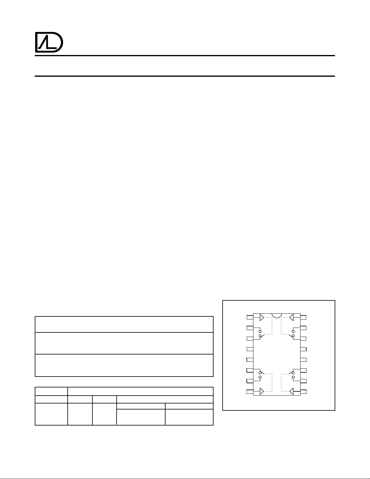
PIN CONFIGURATION/ BLOCK DIAGRAM
ORDERING INFORMATION
Operating Temperature Range
-55°C to +125°C -40°C to +85°C -40°C to +85°C
16-Pin 16-Pin 16-Pin
CERDIP Plastic Dip SOIC
Package Package Package
ALD4211 DC ALD4211 PC ALD4211 SC
ALD4212 DC ALD4212 PC ALD4212 SC
ALD4213 DC ALD4213 PC ALD4213 SC
LOGIC TABLE
Input Logic Switch State
ALD4211 ALD4212 ALD4213
Switch 1 / Switch 4 Switch 2 / Switch 3
COM
OUT
GND
OUT
COM
IN
1
IN
1
2
1
3
1
-
4
V
5
6
4
7
4
8
4
DC, PC, SC PACKAGE
IN
16
2
COM
15
14
13
12
11
10
9
OUT
+
V
NC
OUT
COM
IN
3
2
2
3
3
0 On Off Off On
1 Off On On Off
* Contact factory for industrial temperature range.
© 1998 Advanced Linear Devices, Inc. 415 T asman Drive, Sunnyvale, California 94089 -1706 Tel: (408) 747-1155 Fax: (408) 747-1286 http://www .aldinc.com
Page 2
ABSOLUTE MAXIMUM RATINGS
Supply voltage, V+ referenced to V
GND -0.3V to +13.2V
Terminal voltage range (any terminal) Note 1 (V- -0.3)V to (V+ +0.3)V
Power dissipation 600 mW
Operating temperature range PC, SC package -40°C to +85°C
Storage temperature range -65°C to +150°C
Lead temperature, 10 seconds +260°C
DC current (any terminal) 10mA
-
-0.3V to +13.2V
DC package -55°C to +125°C
POWER SUPPLY RANGE
4211/4212/4213 (PC,SC) 4211/4212/4213 (DC)
Parameter Symbol Min Typ Max Min Typ Max Unit
Supply V
SUPPLY
±1.5 ±6.0 ±1.5 ±6.0 V Dual Supply
Voltage 3.0 12.0 3.0 12.0 V Single Supply
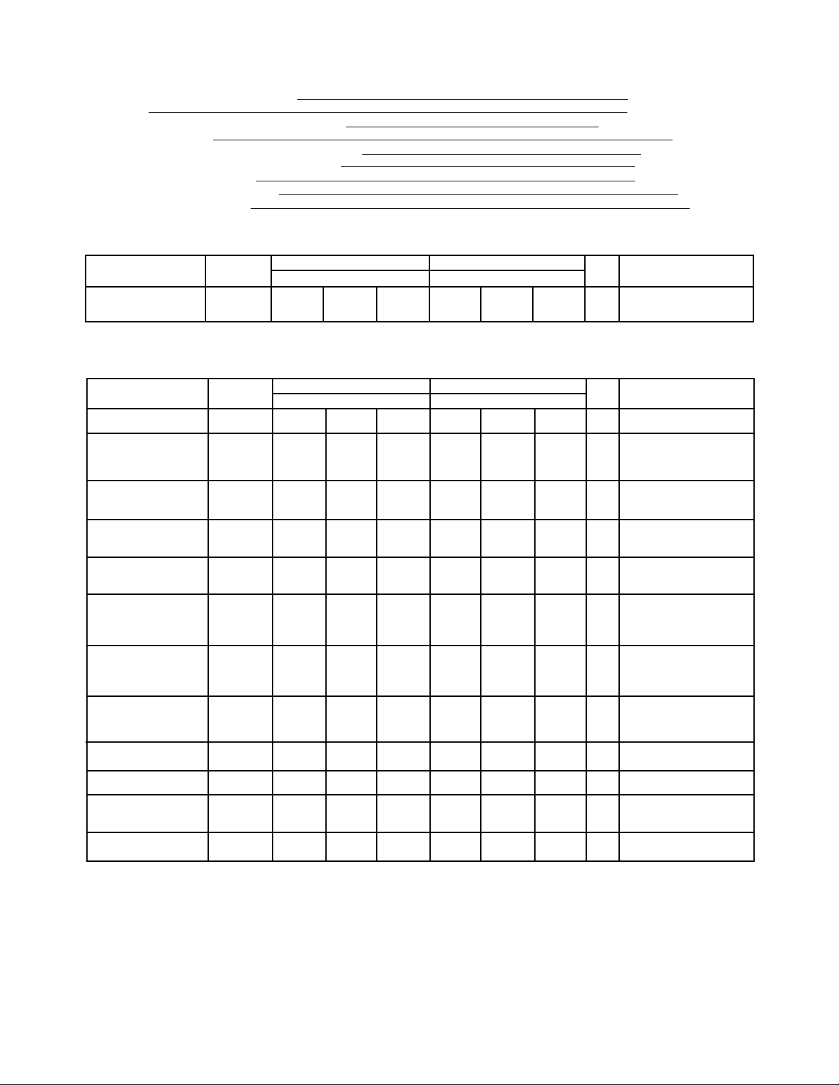
DC ELECTRICAL CHARACTERISTICS
= 25°C V+ = +5.0V, V- = -5.0V GND = 0.0V unless otherwise specified
T
A
4211/4212/4213 (PC,SC) 4211/4212/4213 (DC)
Parameter Symbol Min Typ Max Min Typ Max Unit Test Conditions
Analog Signal Range V
A
-5.0 5.0 -5.0 5.0 V
On - Resistance R
ON
90 135 90 135 Ω VA = 0V IA = 1mA
120 190 -40°C to +85°C
140 210 -55°C to +125°C
Change of On-Resistance ∆R
from -VS to +V
Change of On-Resistance ∆R
with Temperature
S
ON
/∆T 0.43 0.43 %/°C
ON
16 16 %
RON Match between 2 2 %
Switches
Off Com Leakage I
COML
50 100 50 100 pA V
COM
= ±4.0V,V
Current 500 pA -40°C to +85°C
4000 pA -55°C to +125°C
Off Out Leakage I
OUTL
50 100 50 100 pA V
OUT
= ±4.0V, V
Current 500 pA -40°C to +85°C
4000 pA -55°C to +125°C
On Channel I
Leakage Current 500 pA -40°C to +85°C
D(ON)
50 100 50 100 pA
4000 pA -55°C to +125°C
Input High Voltage V
Input Low Voltage V
Input High or I
Input Low Current I
Supply Current I
IH
IL
H
IL
SUPPLY
4.0 4.0 Logic "1"
0.8 0.8 V Logic "0"
10 10 nA
0.01 1 0.01 1 µA
OUT
COM
= -/+4.0V
= -/+4.0V
ALD4211/ALD4212 Advanced Linear Devices 2
ALD4213
Page 3
AC ELECTRICAL CHARACTERISTICS
= 25°C V+ = +5.0V, V- = -5.0V, GND = 0.0V unless otherwise specified
T
A
4211/4212/4213(PC) 4211/4212/4213(DC) 4211/4212/4213(SC)
Parameter Symbol Min Typ Max Min Typ Max Min Typ Max Unit Test Conditions
Turn On
Delay time t
ON
60 130 60 130 60 130 ns (Note 2)
Turn Off
Delay time t
Charge Injection Q
OFF
INJ
60 130 60 130 60 130 ns (Note 2)
0.2 1.0 0.2 1.0 0.2 1.0 pC (Note 3) (Note 4)
Off Isolation 75 75 75 dB At f = 100KHz, (Note 5)
Crosstalk 90 90 90 dB At f = 100KHz, (Note 6)
Total Harmonic T
Distortion 0.01 0.01 0.01 R
Com/Out
Off Capacitance OUT
HD
COM
(OFF)
(OFF)
0.05 0.05 0.05 % RL = 10K
= 100K
L
3.0 3.0 3.0 pF
Channel On
Capacitance C
DS (ON)
5.7 5.7 5.7 pF
Pin to Pin
Capacitance C
PP
0.5 0.6 0.25 pF
DC ELECTRICAL CHARACTERISTICS
= 25°C V+ = +5.0V, V- = GND = 0.0V unless otherwise specified
T
A
4211/4212/4213 (PC,SC) 4211/4212/4213 (DC)
Parameter Symbol Min Typ Max Min Typ Max Unit Test Conditions
Analog Signal Range V
A
0.0 +5.0 0.0 +5.0 V
On - Resistance R
ON
195 280 195 280 Ω VA = 0V IA = 1mA
250 365 -40°C to +85°C
270 390 -55°C to +125°C
Change of On-Resistance ∆R
from -VS to +V
Change of On-Resistance ∆R
with Temperature
S
ON
/∆T 0.43 0.43 %/°C
ON
20 20 %
RON Match 2 2 %
Between Switches
Off Com Leakage I
COML
50 100 50 100 pA V
COM
= +/-4.0V,V
Current 500 pA -40°C to +85°C
4000 pA -55°C to +125°C
Off Out Leakage I
OUTL
50 100 50 100 pA V
Current 500 pA -40°C to +85°C
OUT
= +/-4.0V,V
4000 pA -55°C to +125°C
On Channel I
D(ON)
50 100 50 100 pA
Leakage Current 500 pA -40°C to +85°C
4000 pA -55°C to +125°C
Input High Voltage V
Input Low Voltage V
Input High or I
Input Low Current I
Supply Current I
IH
IL
IH
IL
SUPPLY
4.0 4.0 Logic "1"
0.8 0.8 V Logic "0"
10 10 nA
0.01 1 0.01 1 µA
OUT
COM
= -/+4.0V
= -/+4.0V
Notes: 1. Voltage on any terminal must be less than (V+) + 0.3V and greater than (V-) - 0.3V, at all times including before power is applied and V+ =V- = 0.0V. Vsupply
power supply needs to be sequenced on first on power turn-on and sequenced off last during power turn-off. 2. See Switching Time Test Circuit. Break-before-make time is
not guaranteed. Turn on and turn off time may overlap. 3. Guaranteed by design. 4. See Charge Injection Test Circuit 5. See Off Isolation Test Circuit 6. See Crosstalk
Test Circuit. 7. See switching time test circuit.
ALD4211/ALD4212 Advanced Linear Devices 3
ALD4213
Page 4

AC ELECTRICAL CHARACTERISTICS
ON
OFF
BD
INJ
HD
COM
DS (ON)
- =
GND = 0.0V unless otherwise specified
4211/4212/4213 (PC) 4211/4212/4213 (DC) 4211/4212/4213 (SC)
85 170 85 170 85 170 ns (Note 7)
46 90 46 90 46 90 ns (Note 7)
15 40 15 40 15 40 ns
0.2 1.0 0.2 1.0 0.2 1.0 pC (Note 3) (Note 4)
0.05 0.05 0.05 % RL = 10K
(OFF)
(OFF)
3.0 3.0 3.0 pF
5.7 5.7 5.7 pF
= 100K
L
= 25°C V+ = +5.0V, V
T
A
Parameter Symbol Min Typ Max Min Typ Max Min Typ Max Unit Test Conditions
Turn On
Delay time t
Turn Off
Delay time t
Break-Before-Make
Delay Time t
Charge Injection Q
Off Isolation 75 75 75 dB At f = 100KHz, (Note 5)
Crosstalk 90 90 90 dB At f = 100KHz, (Note 6)
Total Harmonic T
Distortion 0.01 0.01 0.01 R
Com/Out
Off Capacitance OUT
Channel On C
Capacitance
Pin to Pin C
Capacitance
PP
0.5 0.6 0.25 pF
The ALD4211/ALD4212/ALD4213 feature very high
precision due to these factors:
1. The analog switch has ultra low capacitive charge coupling
so that the charge stored on a 200pF sampling capacitor
is minimally affected.
2. With special charge balancing and charge cancellation
circuitry designed on chip, the ALD4211/ALD4212/
ALD4213 achieves ultra low charge injection of typically
only 0.2pC resulting in extremely low signal distortion to
the external circuit.
3. The analog switch switching transistors have pA leakage
currents minimizing the droop rate of the sampling circuit.
4. The internal switch timing allows for the analog switch to
turn off internally without producing any residual transistor
channel charge injection, which may affect external
circuits. With a low loss polystyrene or polypropylene
sampling capacitor, long data retention times are possible
without significant signal loss.
The ALD4211/ALD4212/ALD4213 CMOS analog switches,
when used with industry standard pinout connection, have
the input and output pins reversed with the signal source
input connected to OUT pins and COM pins used as output
pins. In this connection and when used with 1,000pF or
greater value capacitors, or when connected to a DC current
or resistive load, the switch would not be operating in an ultra
low charge injection mode. Typical charge injection, in this
case, would be 5pC as the pin to pin capacitive coupling
effect would dominate. In this connection, all the other
characteristics of the ALD4211/ALD4212/ALD4213 CMOS
analog switches remain the same.
ALD4211/ALD4212 Advanced Linear Devices 4
ALD4213
Page 5

DC ELECTRICAL CHARACTERISTICS
= 25°C V+ = +3.0V, V- = GND = 0.0V unless otherwise specified
T
A
4211/4212/4213 (PC,SC) 4211/4212/4213 (DC)
Parameter Symbol Min Typ Max Min Typ Max Unit Test Conditions
Analog Signal Range V
On - Resistance R
A
ON
0.0 3.0 0.0 3.0 V
500 700 500 700 Ω VA = 0V IA = 1mA
620 880 -40°C to +85°C
680 1000 -55°C to +125°C
Change of On-Resistance ∆R
from -VS to +V
Change of On-Resistance
with Temperature
S
∆RON/∆T 0.27 0.27 %/°C
ON
43 43 %
RON Match 2 2 %
Between Switches
Off Com I
Leakage Current 500 pA -40°C to +85°C
COML
50 100 50 100 pA V
COM
= ±4.0V,V
4000 pA -55°C to +125°C
Off Out I
OUTL
50 100 50 100 pA V
OUT
= ±4.0V,V
Leakage Current 500 pA -40°C to +85°C
4000 pA -55°C to +125°C
Channel On I
D(ON)
50 100 50 100 pA
Leakage Current 500 pA -40°C to +85°C
4000 pA -55°C to +125°C
Input High Voltage V
Input Low Voltage V
Input High or I
Input Low Current I
Supply Current I
IH
IL
IH
IL
SUPPLY
4.0 4.0 Logic "1"
0.8 0.8 V Logic "0"
10 10 nA
0.01 1 0.01 1 µA
AC ELECTRICAL CHARACTERISTICS
-
= 25°C V+ = +3.0V, V
T
A
Parameter Symbol Min Typ Max Min Typ Max Min Typ Max Unit Test Conditions
Turn On Delay time t
=
GND = 0.0V unless otherwise specified
4211/4212/4213 (PC) 4211/4212/4213 (DC) 4211/4212/4213 (SC)
ON
160 300 160 300 160 300 ns (Note 7)
OUT
COM
= -/+4.0V
= -/+4.0V
Turn Off Delay time t
Break-Before-Make t
Delay Time
Charge Injection Q
OFF
BD
INJ
78 1500 78 150 78 150 ns (Note 7)
20 82 20 82 20 82 ns
0.2 0.5 0.2 0.5 0.2 0.5 pC (Note 3) (Note 4)
Off Isolation 75 75 75 dB At f = 100KHz, (Note 5)
Crosstalk 90 90 90 dB At f = 100KHz, (Note 6)
Total Harmonic T
Distortion 0.01 0.01 0.01 R
Com/Out
Off Capacitance OUT
Channel On C
Capacitance
Pin to Pin C
Capacitance
HD
COM
DS (ON)
PP
(OFF)
(OFF)
0.05 0.05 0.05 % RL = 10K
= 100K
L
3.0 3.0 3.0 pF
5.7 5.7 5.7 pF
0.5 0.6 0.25 pF
ALD4211/ALD4212 Advanced Linear Devices 5
ALD4213
Page 6

TYPICAL PERFORMANCE CHARACTERISTICS
POWER DISSIPATION AS A
FUNCTION OF FREQUENCY
1.0
V
0.8
0.6
0.4
0.2
POWER DISSIPATION (mW)
0
0
= 5V
SUPPLY
110
ON RESISTANCE AS A
FUNCTION OF SIGNAL VOLTAGE
500
400
V
= 5V
SUPPLY
100
FREQUENCY (KHz)
1000
10000
ON RESISTANCE AS A
FUNCTION OF SIGNAL VOLTAGE
240
200
V
160
120
80
ON - RESISTANCE (Ω)
40
02
SUPPLY
= 10V
4
SIGNAL VOLTAGE (V)
68
125°C
85°C
25°C
-25°C
-55°C
10
ON RESISTANCE AS A
FUNCTION OF SIGNAL VOLTAGE
850
700
V
SUPPLY
= 3V
300
200
100
ON - RESISTANCE (Ω)
0
01
SWITCH DELAY TIME AS A FUNCTION
OF SUPPLY VOLTAGE
250
200
150
100
50
SWITCH DELAY TIME (ns)
0
3
4
2
SIGNAL VOLTAGE (V)
TURN ON DELAY TIME
TURN OFF DELAY TIME
6
5
SUPPLY VOLTAGE (V)
34
ALD 4211
ALD4213, SW2, 3
7
125°C
85°C
25°C
- 25°C
- 55°C
5
9 10
8
550
400
ON - RESISTANCE (Ω)
250
100
0
0.6
SWITCH DELAY TIME AS A FUNCTION
OF SUPPLY VOLTAGE
250
200
150
100
50
SWITCH DELAY TIME (ns)
0
3
4
6
1.8 2.4
ALD4212
ALD4213 SW1, 4
7
1.2
SIGNAL VOLTAGE (V)
TURN ON DELAY TIME
TURN OFF DELAY TIME
5
SUPPLY VOLTAGE (V)
8
125°C
85°C
25°C
- 25°C
- 55°C
3.0
9 10
ALD4211/ALD4212 Advanced Linear Devices 6
ALD4213
Page 7

TYPICAL PERFORMANCE CHARACTERISTICS
SUPPLY CURRENT AS A
FUNCTION OF INPUT VOLTAGE
2.0
1.6
V
1.2
0.8
0.4
SUPPLY CURRENT (µA)
0
0
SUPPLY
2
= 10V
4
INPUT VOLTAGE (V)
6
8
10
100
80
60
40
20
SUPPLY CURRENT (µA)
0
01
SUPPLY CURRENT AS A
FUNCTION OF INPUT VOLTAGE
10
8
V
6
SUPPLY
= 3V
100
10
1
SUPPLY CURRENT AS A
FUNCTION OF INPUT VOLTAGE
V
SUPPLY
= 5V
2
INPUT VOLTAGE (V)
3
4
TOTAL HARMONIC DISTORTION AS
A FUNCTION OF FREQUENCY
V
V
RL = 10K
SUPPLY
= 0.355 V
S
= 5V
RMS
5
4
SUPPLY CURRENT (µA)
2
0
0
0.6
SWITCH DELAY TIME AS A
FUNCTION OF TEMPERATURE
250
200
150
100
SWITCH DELAY TIME (ns)
NC: Normally Closed
NO: Normally Open
50
0
-75
-25
1.2
INPUT VOLTAGE (V)
TURN ON DELAY TIME
TEMPERATURE (°C)
1.8
V
SUPPLY
TURN OFF DELAY TIME
25
2.4
= 5V
75
3.0
NC
NO
NO
NC
100
0.1
0.01
0.001
TOTAL HARMONIC DISTORTION (%)
0.1
1.0 10
FREQUENCY (KHz)
CHARGE INJECTION AS A FUNCTION
OF SOURCE RESISTANCE
3.0
2.5
2.0
0
0
CL = 1000pF
10
20
SOURCE RESISTANCE (Ω)
1.5.
1.0
0.5
CHARGE INJECTION (PC)
RL = 100K
CL = 200pF
30
100
40
50
ALD4211/ALD4212 Advanced Linear Devices 7
ALD4213
Page 8

TEST CIRCUITS
CC S
4211.STTC.E
4211.THDTC.EPS.W
4211.CITC.EP
Vi = 1Vr ms
100kHz
50Ω
Vi = 1Vrms
100kHz
CROSSTALK TEST CIRCUIT
V+
GND
V-
R
L
V-
OUT1
OUT2
= 1KΩ
O
/Vi ]
R
C
= 1KΩ
L
= 15pF
L
V+
COM1
COM2
CCRR = 20 log [ V
OFF ISOLATION TEST CIRCUIT
50Ω
V+
COM1
IN1
V+
GND
V-
V-
OUT1
=
R
L
1KΩ
C
L
C
L
= 15pF
V
O
= 15pF
V
O
= 3V
V
S
Logic Input
100kHz
4.5V
0V
Logic Input
V
O
SWITCHING TIME TEST CIRCUIT
t
on
COM1
50%
/ t
V+
IN1
90%
off
V+
GND
V-
R
L
V-
OUT1
= 1KΩ
50%
t
/ t
off
on
= tf ≤ 20ns
t
r
10%
C
L
V
O
= 35pF
= 20 log (VO/Vi)
Q
IRR
CHARGE INJECTION TEST CIRCUIT
V+
V-
V+
COM1
IN1
GND
4.5V
0.5V
Logic Input
100kHz
Logic Input
V
O
∆V
O
V-
OUT1
V
O
C
= 200pF
L
∆Q = CL∆V
TOTAL HARMONIC DISTORTION
TEST CIRCUIT
V+
Vi = 1Vpp
50Ω
COM1
IN1
100kHz
O
V+
GND
V-
V-
OUT1
R
=
L
1KΩ
C
= 15pF
L
V
O
ALD4211/ALD4212 Advanced Linear Devices 8
ALD4213
 Loading...