

Datasheet ALD2302SA, ALD2302PA, ALD2302DA, ALD2302ASA, ALD2302APA Datasheet (Advanced Linear Devices Inc)
...Page 1
ADVANCED
LINEAR
DEVICES, INC.
ALD2302A/ALD2302
DUAL PRECISION CMOS VOLTAGE COMPARATOR WITH PUSH-PULL DRIVER
GENERAL DESCRIPTION
The ALD2302A/ALD2302 are monolithic precision high performance
dual voltage comparators built with advanced silicon gate CMOS technology. The primary features are: very high typical input impedance of
12
10
Ω; low input bias current of 10pA; fast response time of 180ns; very
low power dissipation of 175µA per comparator; and single (+5V) or dual
(±5V) power supply operation.
The input voltage range includes ground, which makes these comparators ideal for single supply low level signal detection with high source
impedance. The outputs can source and sink current allowing for
application flexibility. They can be used in either wired-OR connection
without pull-up resistor or push-pull configuration. The ALD2302A/
ALD2302 can also be used in wired-OR connection with other open
drain circuits such as the ALD2301/ALD2303 voltage comparators.
The ALD2302A/ALD2302 voltage comparators are ideal for a great
variety of applications, especially in low level signal detection circuits
which require low standby power and high output current. For quad
packages, use the ALD4302 quad voltage comparator.
APPLICATIONS
• PCMCIA instruments
• MOSFET driver
• High source impedance voltage
comparison circuits
• Multiple limit window comparator
• Power supply voltage monitor
• Photodetector sensor circuit
• High speed LED driver
• Oscillators
• Battery operated instruments
• Remote signal detection
• Multiple relay drivers
FEATURES
• Guaranteed to drive 200Ω loads
• Fanout of 30LS TTL loads
• Low supply current of 175µA each comparator
• Pinout of LM193 type industry standard
comparators
• Extremely low input bias currents -- 10pA
• Virtually eliminates source impedance effects
• Low operating supply voltage of 4V to 12V
• Single (+5V) and dual supply (±5V) operation
• High speed for both large and small signals -180ns for TTL inputs and 400ns for 20mV
overdrive
• CMOS, NMOS and TTL compatible
• Push-pull outputs-current sourcing/ sinking
• High output sinking current -- 60mA
• Low supply current spikes
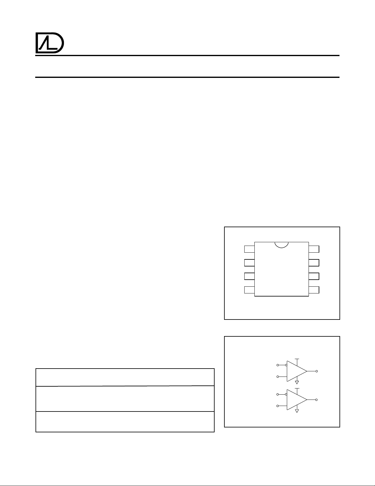
PIN CONFIGURATION
OUT
-IN
+IN
GND
1
1
2
1
3
1
4
TOP VIEW
DA, PA, SA PACKAGE
+
8
V
7
OUT
2
-IN
6
5
+IN
2
2
BENEFITS
• On-chip input and output buffers
• Precision voltage comparison capability
BLOCK DIAGRAM
• Eliminate need for second power supply
• Eliminate pull-up resistor
+
ORDERING INFORMATION
Operating Temperature Range *
-55°C to +125°C 0°C to +70°C 0°C to +70°C
8-Pin 8-Pin 8-Pin
CERDIP Small Outline Plastic Dip
Package Package (SOIC) Package
INVERTING INPUT
-IN
NONINVERTING INPUT
+IN
INVERTING INPUT
-IN
NONINVERTING INPUT
+IN
(2)
1
(3)
1
(6)
2
(5)
2
ALD2302A DA ALD2302A SA ALD2302A PA
ALD2302 DA ALD2302 SA ALD2302 PA
* Contact factory for industrial temperature range
© 1998 Advanced Linear Devices, Inc. 415 T asman Drive, Sunnyvale, California 94089 -1706 Tel: (408) 747-1155 Fax: (408) 747-1286 http://www .aldinc.com
(8) V
+
V
(4) GND
(1) OUT 1
(7) OUT
2
Page 2

ABSOLUTE MAXIMUM RATINGS
Supply voltage, V
Differential input voltage range -0.3V to V
+
13.2V
+
+0.3V
Power dissipation 600 mW
Operating temperature range PA, SA package 0°C to +70°C
DA package -55°C to +125°C
Storage temperature range -65°C to +150°C
Lead temperature, 10 seconds +260°C
OPERATING ELECTRICAL CHARACTERISTICS
+
= 25°C V
T
A
Parameter Symbol Min Typ Max Min Typ Max Unit Conditions
Voltage V
Supply V
Supply I
Current
Voltage A
Gain
Input Offset V
Voltage 2.0 5.0 0°C ≤ T
Input Offset I
1
Current
Input Bias I
1
Current
= +5V unless otherwise specified
2302A 2302 Test
±2 ±6 ±2 ±6 V Dual Supply
4 12 4 12 V Single Supply
350 500 350 500 µARLOAD = ∞
10 100 10 100 V/mV RLOAD ≥15KΩ
0.5 1.0 1.5 4.0 mV RLOAD =1.5KΩ
10 200 10 200 pA 0°C ≤ TA ≤ 70°C
10 200 10 200 pA 0°C ≤ TA ≤ 70°C
1000 1000
S
OS
B
S
+
VD
OS
800 800
≤ 70°C
A
Common
Mode Input V
Voltage
2
Range
ICR
-0.3 V
Low Level I
Output V
OL
0.18 0.4 0.18 0.4 V V
+
-1.5 -0.3 V
+
-1.5 V
SINK
INPUT
Voltage Differential
Low Level
Output I
OL
24 60 24 60 mA V
OL
Current
High Level
Output V
Voltage
Response C
2
Time
OH
t
RP
3.5 4.5 3.5 4.5 V IOH = -2mA
=15pF
L
400 400 ns 100mV Input
Step/20mV
Overdrive
= 15pF
C
180 180 ns TTL- Level Input
L
Step
Notes:1 Consists of junction leakage currents
2
Sample tested parameters
=12mA
=1V
=1.0V
ALD2302A/ALD2302 Advanced Linear Devices 2
Page 3

TYPICAL PERFORMANCE CHARACTERISTICS
SATURATION VOLTAGE
vs. TEMPERATURE
1.4
VS = ± 2.5V
1.2
I
= 50mA
SINK
1.0
0.8
0.6
0.4
0.2
SATURATION VOLTAGE (V)
0
-55 -25 0 25 50 12510075
TEMPERATURE (°C)
COMMON - MODE VOLTAGE REFERRED
TO SUPPLY VOLTAGE
0.5
V+
-0.5
-1.0
0.5
V-
-0.5
COMMON - MODE VOLTAGE LIMITS (V)
VS = ± 2.5 V
-55 -25 0 25 50 12510075
TEMPERATURE (°C)
TRANSFER FUNCTION
+6.0
TA = 25°C
V
= ±6V
S
0.0
OUTPUT VOLTAGE (V)
-6.0
-2.5
0.0
+2.5
DIFFERENTIAL INPUT VOLTAGE (mV)
RESPONSE TIME FOR VARIOUS
INPUT OVERDRIVES
0
V
V+
100
IN
INPUT
VOLTAGE (mV)
≈≈
+2.5
0.0
0V
TTL
50mV
V
+
OUT
-
V-
OUTPUT
VOLTAGE (V)
-2.5
0.0 0.1 0.2 0.40.3 0.60.5 0.7
TIME (µs)
TA = 25°C
V
= ±2.5V
S
20mV
≈≈
10mV
SATURATION VOLTAGE vs.
1.5
1.2
0.9
0.6
VOLTAGE (V)
OUTPUT SATURATION
0.3
0.0
VS = ±2.5V
0 1530456075
OUTPUT SINK CURRENT (mA)
SINK CURRENT
125°C
85°C
25°C
-25°C
-55°C
100
0
INPUT
VOLTAGE (mV)
+2.5
0.0
OUTPUT
-2.5
VOLTAGE (V)
RESPONSE TIME FOR VARIOUS
INPUT OVERDRIVES
TA = 25°C
V
= ±2.5V
S
V
V+
IN
0V
TTL
0.0 0.1 0.2 0.40.3 0.60.5 0.7
V
+
OUT
-
V-
10mV
20mV
50mV
TIME (µs)
≈≈
ALD2302A/ALD2302 Advanced Linear Devices 3
Page 4

TYPICAL PERFORMANCE CHARACTERISTICS
TOTAL SUPPLY CURRENT vs.
TOTAL SUPPLY VOLTAGE
+
500
V
-
+
400
300
200
SUPPLY CURRENT (µA)
100
4.02.0
6.0
8.0
SUPPLY VOLTAGE (V)
NORMALIZED INPUT OFFSET VOLTAGE
vs. TEMPERATURE
+3
+2
+1
V
CM
V
S
T
= 25°C
A
R
=
L
10.0
= 0V
= ±2.5V
SUPPLY CURRENT vs. TEMPERATURE
550
500
∞
450
VS = ±2.5V
No Load
All comparators
400
350
300
SUPPLY CURRENT (µA)
250
200
12.0
-55
-25
025
50
100
75
125
TEMPERATURE (°C)
INPUT OFFSET VOLTAGE vs. SUPPLY
VOLTAGE REPRESENTATIVE SAMPLES
6
4
2
T
= 25°C
A
0
-1
VOLTAGE (mV)
-2
NORMALIZED INPUT OFFSET
-3
-55 -25 0 25 50 12510075
TEMPERATURE (°C)
OUTPUT HIGH VOLTAGE
+
V
-0.6
(V)
+
+
V
-0.5
+
-0.4
V
+
V
-0.3
+
-0.2
V
+
-0.1
V
+
V
OUTPUT HIGH VOLTAGE FROM V
2
vs. SUPPLY VOLTAGE
4
SUPPLY VOLTAGE (V)
TA = 25°C
IOH = -2mA
6
8
10
12
0
-2
-4
INPUT OFFSET VOLTAGE (mV)
-6
2
4
6
SUPPLY VOLTAGE (V)
OUTPUT LOW VOLTAGE
vs. SUPPLY VOLTAGE
0.6
0.5
0.4
0.3
0.2
0.1
OUTPUT LOW VOLTAGE (V)
0.0
2
4
6
SUPPLY VOLTAGE (V)
8
8
10
TA = 25°C
I
= 12mA
OL
10
12
12
ALD2302A/ALD2302 Advanced Linear Devices 4
Page 5

TYPICAL APPLICATIONS
ZERO CROSSING DETECTOR
DOUBLE DUAL LIMIT WINDOW COMPARATOR
+3V
ALD2302
50K
V
V
IN
+
OUT
-5V
50K
+12V
VH
+12V
2
+
+12V
1/2 ALD2302
VH
V
MULTIPLE RELAY DRIVE
REF
V
IN
+
+5V
+5V
47K
V
VL
1
IN
1
+
+12V
+12V
+
1/2 ALD2302
VOLTAGE LEVEL TRANSLATOR
V+ = +10V
V
REF
V
IN
+
1/2 ALD2302
V
= 1.4V for TTL input
REF
+
V
V
REF
Output V
=
OUT
for CMOS input
2
swings from rail-to-rail
V
OUT
+
VL
50K
VL1 and VH1 first limit window send warning
and VH2 second limit window execute
VL
2
system cutoff
2
ALD2302
ALD2302A/ALD2302 Advanced Linear Devices 5
Page 6

TYPICAL APPLICATIONS
PUSH-PULL COMPLEMENTARY POWER MOSFET DRIVER
This circuit eliminates crossover current in the
complementary power transistors. The outputs can
be used to source and sink different loads or tied
together to provide push-pull drive of the same load.
1/2 ALD 2302
+
V
V
REF
V
IN
+
+12V
+12V
10K
V
1
V
IN
40K
V
2
+
+12V
+
10K
TIME DELAY GENERATOR
+
V
R
F1
R
R
T
C
T
F2
R
F3
ALD2302
1/2 ALD 2302
+
1/2 ALD 2302
+
1/2 ALD 2302
+12V
P- Channel VP 02
Power MOSFET
2A Source
2A Sink
N - Channel VN 01
Power MOSFET
V
1
V
2
V
3
+
R
F4
Design & Operating Notes:
1. As each output sources up to 10mA in the output high state, the output stage of a wired - OR low output circuit must be able to sink this current and still
provide desired output voltage levels. For TTL output levels, this consideration limits the number to a maximum of three ALD2302 outputs wired-OR
together.
2. In order to minimize stray oscillation, all unused inputs must be tied to ground.
3. The input bias and offset currents are essentially input protection diode reverse bias leakage currents, and are typically less than 1 pA at room
temperature. The currents are a function of ambient temperature, and would have to be considered in applications where very high source impedance
or high accuracy are involved.
4. The high output sinking current of 60mA for each output offers flexibility in many applications, as a separate buffer or driver would not be necessary to
drive the intended load. However, as the circuit normally operates close to ambient temperature due to its very low power consumption, thermal effects
caused by large output current transients must be considered in certain applications.
ALD2302A/ALD2302 Advanced Linear Devices 6
 Loading...