

Datasheet ALD1801DC, ALD1801BSC, ALD1801BPC, ALD1801BDC, ALD1801ASC Datasheet (Advanced Linear Devices Inc)
...Page 1
ADVANCED
LINEAR
DEVICES, INC.
ALD1801A/ALD1801B
ALD1801
8 BIT MICROPOWER MULTIPLYING D/A CONVERTER
GENERAL DESCRIPTION
The ALD1801 is an 8-bit monolithic current output digital to analog
converter designed to provide low power, low operating voltage and simple
operation. It offers industry pin configuration of DAC-08 types, and is
intended for a wide range of digital to analog conversion and control
applications in +5V single power supply and ±5V dual power supply
systems, as well as +3V to +12V battery operated systems. Device
characteristics are specified for +5V single supply and 3.3V dual supply
systems.
The ALD1801 is manufactured with Advanced Linear Devices’ enhanced
ACMOS silicon gate CMOS process and has been designed to be also
used as a linear cell element in Advanced Linear Devices’ "FunctionSpecific" ASIC, as it is fully compatible in design, operation, and manufacture
with all other linear elements in Advanced Linear Devices’ product family.
The ALD1801 is designed with matching between reference and full scale
currents. Digital inputs are standard CMOS logic inputs to provide ease
of interface. Output currents can be directly converted to a voltage output
by using a pair of resistors. When used with ALD’s rail-to-rail output
operational amplifiers such as the ALD1702, full scale output of 0 to +5V
can be easily achieved with single +5V power supply.
ORDERING INFORMATION
Operating Temperature Range
-55°C to +125°C0°C to +70°C0°C to +70°C
16-Pin 16-Pin 16-Pin
CERDIP Small Outline Plastic Dip
Package Package(SOIC) Package
ALD1801A DC ALD1801A SC ALD1801A PC
ALD1801B DC ALD1801B SC ALD1801B PC
ALD1801 DC ALD1801 SC ALD1801 PC
FEATURES
• Low voltage 3V to 12V operation
• Low power 1.8mW max @ 3.3V
• Single supply operation (5V or 3.3V)
• Direct CMOS logic interface
• Complementary current outputs
• Nonlinearity to 0.1% max over
temperature range
• High input impedance
• Low full scale current
• High output impedance
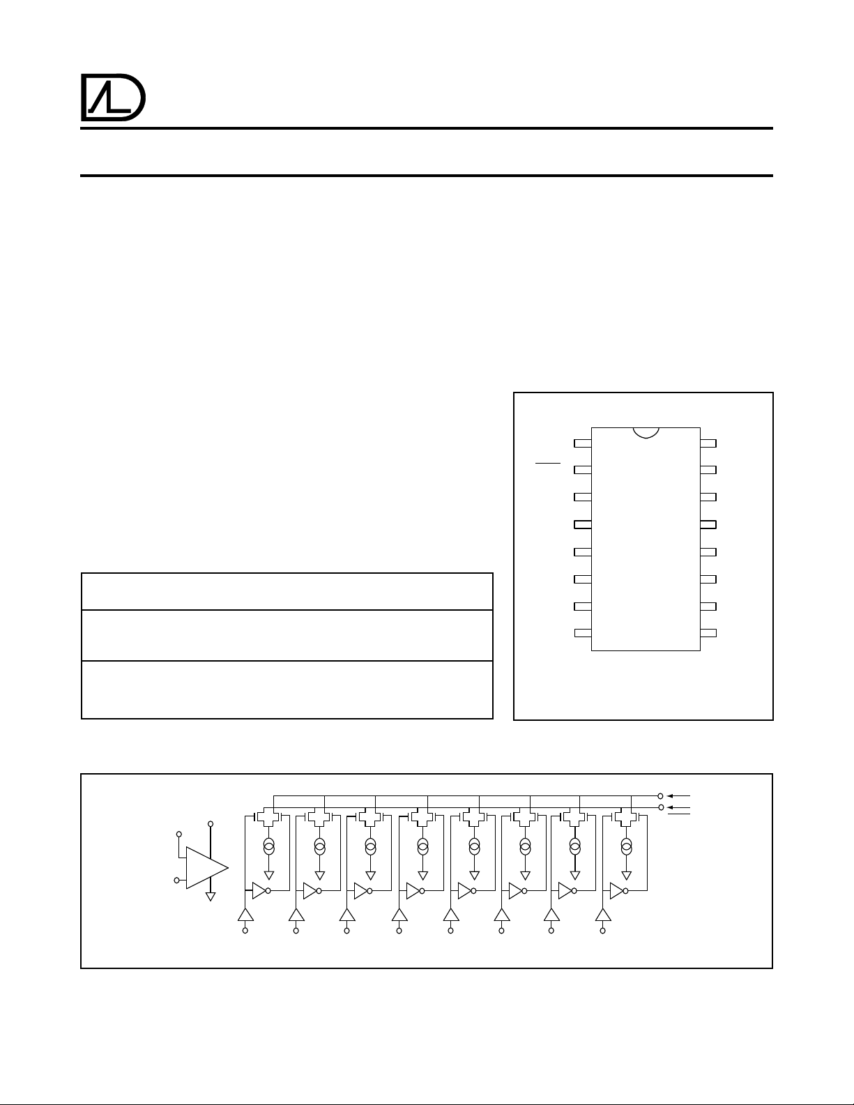
PIN CONFIGURATION
1
N/C N/C
I OUT
MSB B
2
-
V
3
I
4
OUT
5
1
6
B
2
B
7
3
8
B
4
TOP VIEW
DC, PC, SC PACKAGE
* N/C Pin is connected internally. Do not connect externally.
16
15
14
13
12
11
10
9
V
REF-
V
REF+
+
V
B8 LSB
B
7
B
6
B
5
* Contact factory for industrial temperature range
BLOCK DIAGRAM
IOUT
4
2
V
REF+
14
V
REF-
15
© 1998 Advanced Linear Devices, Inc. 415 T asman Drive, Sunnyvale, California 94089 -1706 Tel: (408) 747-1155 Fax: (408) 747-1286 http://www .aldinc.com
V+
13
I
B1
3
5
B
1
MSB
I
B2
6
B
2
I
B3
7
B
3
I
B4
8
B
4
I
B5
9
B
5
I
B6
10
B
6
I
B7
11
B
7
12
B
8
LSB
IOUT
I
B8
Page 2
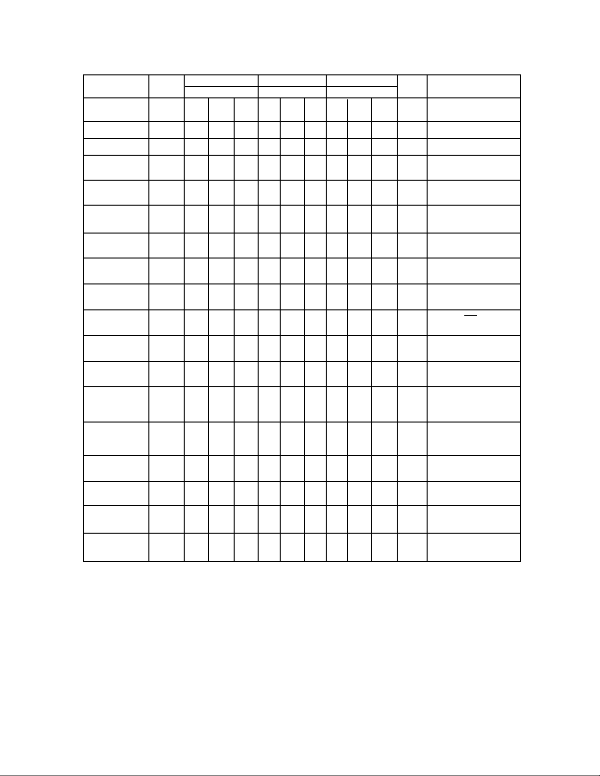
OPERATING ELECTRICAL CHARACTERISTICS
= 25°C VS = ±2.5V or VS = +5.0V unless otherwise specifie
T
A
1801A 1801B 1801
Parameter Symbol Min Typ Max Min Typ Max Min Typ Max Unit Test Conditions
Supply V
Voltage Single Supply
S
Resolution 8 8 8 Bits
Monotonicity 8 8 8 Bits
±1.5 ±6.0 ±1.5 ±6.0 ±1.5 ±6.0 V Dual Supply
Nonlinearity N
Settling Time t
Propagation t
Delay 1.5 2.5 1.5 2.5 1.5 2.5 µs All Bits
Full Scale T
Tempco
Output V
Compliance +1.5 +0.2 +1.5 +0.2 +1.5 +0.2
L
S
d
C
-
OC
V
±0.1 ±0.19 ±0.39 % of
Full Scale
2.5 5.0 2.5 5.0 2.5 5.0 µs To 1/2 LSB with all bits
turned on/off
1.5 2.5 1.5 2.5 1.5 2.5 µs Each Bit
±10 ±50 ±10 ±50 ±10 ±50 ppm/°C
V+V
-
V+V
-
V+V
Output 50 50 50 MΩ Output Within
Impedance Compliance limits
Full Scale I
Current Range V
Full Scale I
Symmetry
Zero Scale I
Current
Logic Input Level
Logic "0" V
Logic "1" V
FS
FSS
ZS
1
IL
IH
100 100 100 µAR
±2.5 ±2.5 ±2.5 µA
10 10 10 nA
-1.1 -1.1 -1.1 V Supply = ±2.5V
2.1 2.1 2.1
OUT
REF
= R
OUT
= 2.5V; R
Logic Swing
Logic Threshold V
Range -1.5 1.5 -1.5 1.5 -1.5 1.5 V Supply = ±2.5V
LS
-2.8 2.8 -2.8 2.8 -2.8 2.8 V Supply = ±2.5V
= 50KΩ
=25KΩ
REF
Reference Bias I
Current
Power Supply +I
Current - I
Power Dissipation P
RB
S
S
D
0.1 0.1 0.1 nA
500 800 500 800 500 800 µA Full Scale
700 1000 700 1000 700 1000 Output = 100µA
4.5 4.5 4.5 mW Supply = ±2.5V
Compensation Not Required
Notes: 1. Contact ALD for ±1.0V/±1.25V operation
2. Logic levels of V
0.4V and VIH 4.6V for single supply applications.
IL
ALD1801A/ALD1801B Advanced Linear Devices 2
ALD1801
Page 3

OPERATING ELECTRICAL CHARACTERISTICS
T
= 25°C VS = ±1.65V or VS = +3.3V unless otherwise specified
A
1801A 1801B 1801
Parameter Symbol Min Typ Max Min Typ Max Min Typ Max Unit Test Conditions
Resolution 8 8 8 Bits
Monotonicity 8 8 8 Bits
Nonlinearity N
Settling Time t
L
S
±0.1 ±0.19 ±0.39 % of
Full Scale
4.0 10.0 4.0 10.0 4.0 10.0 µs To 1/2 LSB with all bits
turned on/off
Propagation t
d
1.5 4.0 1.5 4.0 1.5 4.0 µs Each Bits
Delay 1.5 4.0 1.5 4.0 1.5 4.0 µs All Bits
Full Scale T
C
±10 ±50 ±10 ±50 ±10 ±50 ppm/°C
Tempco
Output V
OC
-
V
V+V
-
V+V
-
V+V
Compliance +1.5 +0.2 +1.5 +0.2 +1.5 +0.2
Output 50 50 50 MΩ Output Within
Impedance Compliance limits
Full Scale I
FS
50 50 50 µAR
Current Range V
Full Scale I
FSS
±2.5 ±2.5 ±2.5 µA
OUT
REF
= R
OUT
= 2.5V; R
= 100KΩ
Symmetry
Zero Scale I
ZS
10 10 10 nA
Current
REF
=50KΩ
Reference Bias I
RB
0.1 0.1 0.1 nA
Current
Power Supply +I
Current - I
Power Dissipation P
S
S
D
350 500 350 500 350 500 µA Full Scale
450 600 450 600 450 600 Output = 50µA
1.8 1.8 1.8 mW
ALD1801A/ALD1801B Advanced Linear Devices 3
ALD1801
Page 4

+V
DUAL SUPPLY ±2.5V
RATIOMETRIC VOLTAGE OUTPUT DAC
50K
V+ = 2.5V
50K
REF
ALD
1702
+
V- = 2.5V
V+ = 2.5V
13
15
14
12
11
10
9
B1
B2
B3
B4
34
2
5
6
7
8
ALD 1801
V
B8
B7
B6
B5
V
OUT
REF-
LSB
25K
+V
REF
=2.5V
Zero Scale 0 0 0 00000-2.500
B1 B2 B3 B4 B5 B6 B7 B8 V
LSB 00000001-2.480
Half Scale -LSB 0 1 1 11111 -0.019
Half Scale 1 0 0 000000.000
Half Scale +LSB 1 0 0 000010.019
Full Scale 1 1 1 111112.480
OUT
SINGLE SUPPLY 3.3V
RATIOMETRIC VOLTAGE OUTPUT DAC
50K
50K
V+
V+ = 3.3V
+
V
OUT
1/2 ALD2701
50K
50K
1/2 ALD2701
+
MSB
0.1µF
B1
B2
B3
B4
2
5
6
7
8
V+
13
34
15
25K
14
+V
= V+
REF
B8
B7
B6
B5
LSB
12
11
10
9
ALD 1801
Zero Scale 0 0 0 000000.000
B1 B2 B3 B4 B5 B6 B7 B8 V
Half Scale 1 0 0 000001.650
Full Scale 1 1 1 111113.287
ALD1801A/ALD1801B Advanced Linear Devices 4
ALD1801
OUT
Page 5

APPLICATIONS NOTES:
The ALD1801 is an 8 bit multiplying D/A converter. It has
been designed to operate with standard single or split
power supplies of 5V or ±5V. Functionality extends down
to 3V or ±1.5V power supply, making it ideal for lithium
battery or rechargeable battery operated systems where
power efficiency and performance are important design
parameters.
The ALD1801 features ultra low quiescent bias current
which depends on the operating current in the internal
current steering circuit. A high gain internal operational
amplifier is fully compensated for stable operation without
any need for external capacitor compensation. The
operational amplifier is placed in a negative feedback loop
to generate the reference current for ratio matched
transistors. It is trimmed to provide nonlinearity as
specified. In some applications this feature can be used
along with the multiplying nature of the ALD1801 to obtain
9 or 10 bit digital to analog conversion with external
switches.
The ALD1801 is a multiplying D/A converter in which the
output is a current that is a function of an 8 bit digital input
word multiplied by the reference current. The reference
current may be a fixed reference current or a varying input
current. If a fixed reference voltage or a varying low
impedance voltage output source is used, a fixed value
resistor (referred to as RREF) can be used to convert
the voltage into a reference current for most applications.
is a precision fixed resistor without trimming.
R
REF
Trimming can be accomplished by adjusting R
REF
through
either connecting a potentiometer in series with a fixed
resistor or by substituting the fixed resistor with a multiturn potentiometer. The recommended nominal value of
is 25KΩ.
R
REF
The ALD1801 can operate from single power supply or
dual supplies up to ±6.6V. Symmetrical supplies are not
required in the case of dual supply operation. However,
input voltage must be set at 1V or higher above the
V
-
REF
V- voltage. Due to the internal operational amplifier
feedback, V
potential as V
input terminal would be set at the same
+
REF
- input terminal, with the input reference
REF
current determined by: Input reference current
I
REF
= { (V
REF+
)- (V
REF-
) } / R
REF
The ALD1801 is fabricated in CMOS technology and
provides direct logic interface to all CMOS logic families
including logic levels of the CD4000 and 74C logic families
operating at logic voltage levels other than 5V. It is
primarily designed to operate in a power supply
environment where interface takes place between digital
logic circuitry and analog circuitry. Both types of circuitry
operate with the same power supplies.
The nonlinearity and monotonicity of the ALD1801 applies
over the full rated operating temperature. The device has
been developed with minimal temperature drift, typically
at ±10ppm/°C. A single array of matched and tracked
resistor networks of nominal 50KΩ can be used for all the
resistors required for the D/A converter. As an example,
can be set to 25KΩ by connecting two 50KΩ resistors
R
REF
in parallel where output resistors are set at 50KΩ.
Due to the very low quiescent and reference currents
used, layout of the circuit board to minimize any parasitic
capacitance is important in getting high frequency
operation, as the settling time is due in large part to the
output currents charging and discharging the node
capacitances at the output. As the internal bias current
levels is adaptive to the reference current, the switching
speed of the device depends on the reference current
selected. Characterization of the settling time has been
performed at full scale current set at 100µA and device
operation at single 5V supply. Faster operation can be
obtained by using short leads, minimizing output
capacitance, load resistor values, and by adequate bypass
capacitors placed on the board at the supply and reference
nodes.
and Io outputs can be used simultaneously. If one
Both I
o
of the outputs is not used, then it must be connected to
ground or a potential where the sum of I
and Io can
o
maintain a constant value. Due to internal leakage currents
that vary with temperature, it is recommended that I
FS
of
50µA to 100µA be used so that 1/2LSB bit current is set at
as high a level as possible. The temperature coefficient
of the reference resistor R
and R
should match to minimize temperature drift.
OUT
and output resistors R
REF
OUT
ALD1801A/ALD1801B Advanced Linear Devices 5
ALD1801
Page 6

TYPICAL PERFORMANCE CHARACTERISTICS
PROPAGATION DELAY (µsec)
PROPAGATION DELAY AS A FUNCTION
OF FULL SCALE OUTPUT CURRENT
1.9
1.7
1.5
1.3
1.1
20 40 60 80 100
OUTPUT CURRENT (µA)
SUPPLY CURRENT AS A FUNCTION
OF SUPPLY VOLTAGE
FULL SCALE
800
T
= 25°C
A
SUPPLY CURRENT AS A FUNCTION
OF TEMPERATURE
I
800
600
400
200
SUPPLY CURRENT (µA)
0
1200
S-
VS = ±2.5V
I
S+
VS = ±2.5V
I
S-
VS = ±1.65V
I
S+
VS = ±1.65V
0 255075100
TEMPERATURE (°C)
ALL BITS "HIGH "
V
= V+
REF
R
= 25K
REF
125-25
FULL SCALE OUTPUT CURRENT
AS A FUNCTION OF SUPPLY VOLTAGE
100
80
I
REF
= 100µA
600
400
200
SUPPLY CURRENT (µA)
0
150
100
50
OUTPUT CURRENT (µA)
I
= 100µA
REF
I
= 0
REF
±1 ±2 ±3 ±4 ±5
SUPPLY VOLTAGE (V)
FULL SCALE OUTPUT CURRENT
AS A FUNCTION OF OUTPUT
VOLTAGE (COMPLIANCE)
VS = ±2.5V
VS = ±1.65V
V
= ±1.65V
VS = ±2.5V
S
I
REF
I
REF
= 100µA
= 50µA
60
I
40
20
0
±60
FULL SCALE OUTPUT CURRENT (µA)
0 ±1 ±2
SUPPLY VOLTAGE (V)
±3
= 50µA
REF
±4 ±5 ±6
FULL SCALE OUTPUT CURRENT
AS A FUNCTION
OF REFRENCE CURRENT
150
VS = ±1.65V TO ±2.5V
125
100
75
50
OUTPUT CURRENT (µA)
25
0
-2 -1
SUPPLY VOLTAGE (V)
+1 +2
0
0
25 50 75 100 125
REFRENCE CURRENT (µA)
1500
ALD1801A/ALD1801B Advanced Linear Devices 6
ALD1801
 Loading...