

Datasheet ALD1110ESC, ALD1110ESA, ALD1110EPC, ALD1110EPA Datasheet (Advanced Linear Devices Inc)
Page 1
FEATURES
•
Operates from 2V, 3V, 5V to 10V
•
Flexible basic circuit building block and design element
•
Very high resolution -- average programmable voltage
resolution of 0.1mV
•
Wide dynamic range -- current levels from 0.1µA
to 3000µA
•
Voltage adjustment range from 1.000V to 3.000V
in 0.1mV steps
•
Proven, non-volatile CMOS technology
•
Typical 10 years drift of less than 2mV
•
Usable in voltage mode or current mode
•
High input impedance -- 1012Ω
•
Very high DC current gain -- greater than 10
9
•
Device operating current has positive temperature
coefficient range and negative temperature
coefficient range with cross-over zero temperature
coefficient current level at 68µA
•
Tight matching and tracking of on-resistance
between different devices with programming
•
Very low input currents and leakage currents
•
Low cost, monolithic technology
•
Application-specific or in-system programming modes
•
User programmable software-controlled automation
•
User programmability of any standard/custom
configuration
•
Micropower operation
•
Available in standard PDIP, SOIC and hermetic
CDIP packages
•
Suitable for matched-pair balanced circuit configuration
•
Suitable for both coarse and fine trimming applications
QUAD/DUAL ELECTRICALLY PROGRAMMABLE ANALOG DEVICE (EPAD™)
ADVANCED
LINEAR
DEVICES, INC.
ALD1108E/ALD1110E
BENEFITS
•
Simple, elegant single-chip solution
to trimming voltage/current values
•
Direct in-circuit active element operation
and programming
•
Remotely and electrically trim parameters on
circuits that are physically inaccessible
•
Usable in environmentally sealed circuits
•
No system overhead or active circuitry required
•
No mechanical moving parts -- high G-shock
tolerance
•
Improved reliability, dependability, dust and
moisture resistance
•
Cost and labor savings
•
Small footprint for high board density
applications
•
Fully automated test and trimming environment
Operating Temperature Range*
-55°C to +125°C0°C to +70°C0°C to +70°C
8-Pin 8-Pin 8-Pin
CERDIP Plastic Dip SOIC
Package Package Package
ALD1110E DA ALD1110E PA ALD1110E SA
Operating Temperature Range*
-55°C to +125°C0°C to +70°C0°C to +70°C
16-Pin 16-Pin 16-Pin
CERDIP Plastic Dip SOIC
Package Package Package
ALD1108E DC ALD1108E PC ALD1108E SC
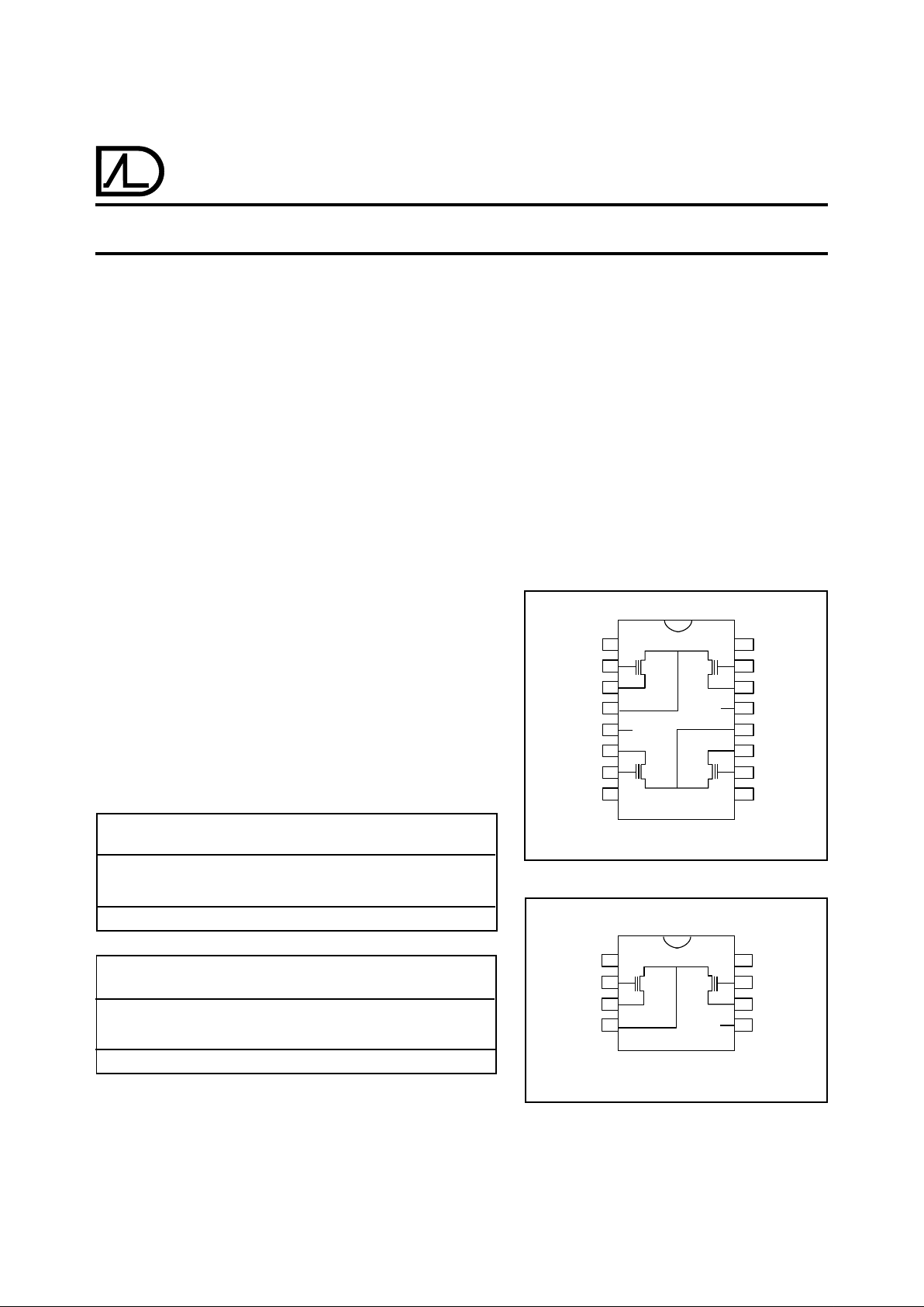
ORDERING INFORMATION
PIN CONFIGURATION
PIN CONFIGURATION
* Contact factory for industrial temperature range
P
N2
1
2
3
14
15
16
4
13
V
+
5
12
S
34
P
N3
6
7
8
10
11
G
N1
D
N1
P
N1
S
12
V
-
G
N4
P
N4
D
N4
9
G
N3
D
N3
D
N2
G
N2
DC, PC, SC PACKAGE
v
-
v
+
ALD1108E
EPAD 1
EPAD 2
EPAD 4
EPAD 3
P
N2
1
2
3
6
7
8
4
5
V
+
G
N1
D
N1
P
N1
S12, V
-
D
N2
G
N2
DA, PA, SA PACKAGE
v
+
ALD1110E
EPAD 1
EPAD 2
© 1998 Advanced Linear Devices , Inc. 415 T asman Dr ive, Sunn yvale, Calif ornia 94089 -1706 T el: (408) 747-1155 F ax: (408) 747-1286 http://www.aldinc.com
Page 2
ALD1108E/ALD1110E Advanced Linear Devices 2
GENERAL DESCRIPTION
ALD1108E/ALD1110E are monolithic quad/dual EPADs (Electrically
Programmable Analog Device) that utilize CMOS MOSFET with electrically programmable threshold voltage. For a given input voltage,
changing the threshold turn-on voltage of a MOSFET device precisely
changes its drain on-current, resulting in an on-resistance characteristic that can be precisely set and controlled. Used as an in-circuit element
for trimming or setting a combination of voltage and/or current characteristics, it can be programmed via a Personal Computer remotely and
automatically via software control. Once programmed and set, the set
voltage and current levels are stored indefinitely inside the device as a
precisely controlled nonvolatile stored charge, which is not affected
during normal operation of the device, even after power has been turned
off.
The ALD1108E/ALD1110E are devices built with ALD's EPAD technology, an electrically programmable device technology refined for analog
applications. The ALD1108E/ALD1110E functions like a regular MOSFET
transistor except with precise user preset threshold voltage. Using the
ALD1108E/ALD1110E is simple and straight forward. The device is
extremely versatile as a circuit element and design component. It
presents the user with a wealth of possible applications, limited only by
the imagination of the user and the many ways an analog MOSFET
device can be used as a circuit design element. The ALD1108E/
ALD1110E do not need other active circuitry for functionality.
The basic device is a monotonically adjustable device which means the
device can normally be programmed to increase in threshold voltage
and to decrease in drain-on current as a function of a given input bias
voltage. Once adjusted, the voltage and current conditions are permanent and not reversible. However, a given EPAD device can be adjusted
many times to continually increase the threshold voltage. A pair of EPAD
devices can also be connected such that one device is used to adjust a
parameter in one direction and the other device is used to adjust the
same parameter in the other direction.
The ALD1108E/ALD1110E can be pre-programmed with the ALD
EPAD programmer to obtain the desired voltage and current levels. Or,
they can be programmed as an active in-system element in a user
system, via user designed interface circuitry. For more information, see
Application Note AN1108.
APPLICATIONS
•
Precision PC-based electronic calibration
•
Automated voltage trimming or setting
•
Remote voltage or current adjustment of
inaccessible nodes
•
PCMCIA based instrumentation trimming
•
Electrically adjusted resistive load
•
Temperature compensated current sources
and current mirrors
•
Electrically trimmed/calibrated current
sources
•
Permanent precision preset voltage level
shifter
•
Low temperature coefficient voltage and/or
current bias circuits
•
Multiple preset voltage bias circuits
•
Multiple channel resistor pull-up or pull-down
circuits
•
Microprocessor based process control systems
•
Portable data acquisition systems
•
Battery operated terminals and instruments
•
Remote telemetry systems
•
Programmable gain amplifiers
•
Low level signal conditioning
•
Sensor and transducer bias currents
•
Neural networks
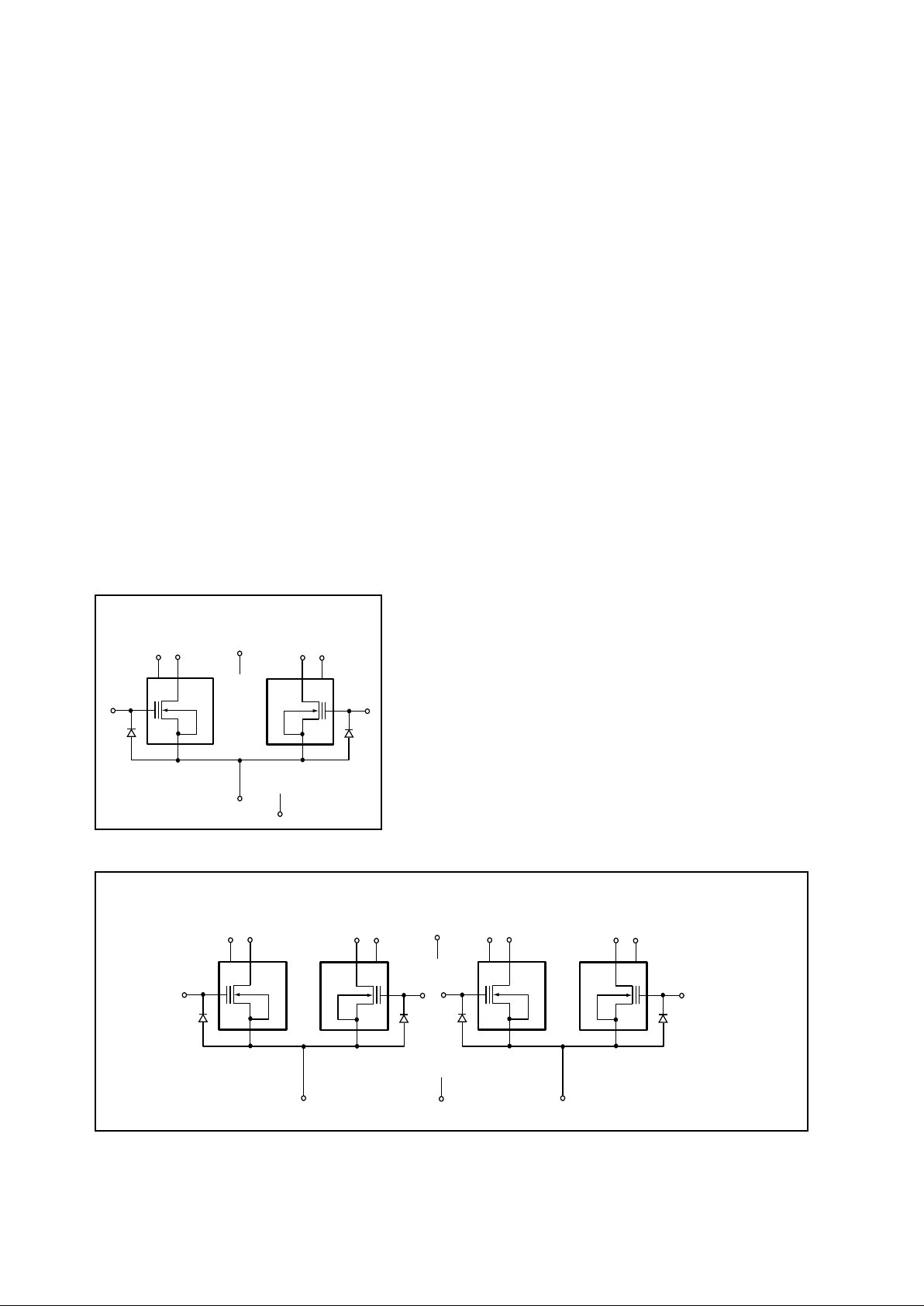
BLOCK DIAGRAM
P
N1
(1) DN1 (3)
G
N1
(2)
D
N2
(6)
P
N2
(8)
G
N2
(7
)
V- (4)
V+(5)
S
12
(4)
ALD1110E
EPAD 1
EPAD 2
~
~
BLOCK DIAGRAM
EPAD 1
EPAD 2 EPAD 3 EPAD 4
PN4 (8)
P
N
(1) DN1 (3)
G
N1
(2)
D
N2
(14)
P
N2
(16)
G
N2
(15)
P
N3
(9)
D
N3
(11)
G
N3
(10)
D
N4
(6)
G
N4
(7)
V- (5)
V+(13)
S
12
(4) S34 (12)
ALD1108E
~
~
Page 3

ALD1108E/ALD1110E Advanced Linear Devices 3
Supply Voltage V
+
1.2 10.0 1.2 10.0 V
Initial Threshold Voltage V
ti
0.990 1.000 1.010 0.990 1.000 1.010 V IDS = 1µA TA = 21°C
Programmable Vt Range V
t 1.000
3.000 1.000 3.000 V
Drain - Gate Connected TCV
DS
-1.6 -1.6 mV/°CI
D
= 5µA
Voltage Tempco -0.3 -0.3 mV/°CI
D
= 50µA
0.0 0.0 mV/°CI
D
= 68µA
+2.7 +2.7 mV/°CI
D
= 500µA
Initial Offset
Voltage V
OSi
15 15mV
Tempco of V
OS
TCV
OS
55µV/°CV
DS1
= V
DS2
Differential Threshold Voltage DV
t
2.000 2.000 V
Tempco of Differential
Threshold Voltage TCDV
t
0.033 0.033 mV/°C
Long Term Drift ∆V
t
/∆t -0.02 -0.05 -0.02 -0.05 mV 1000 Hours
Long Term Drift Match ∆V
t
/∆t-5 -5µV 1000 Hours
Drain Source On Current I
DS(ON)
3.0 3.0 mA VG =VD = 5V VS = 0V
V
t
= 1.0
Drain Source On Current I
DS(ON)
0.8 0.8 mA VG =V
D
=
5V V
S
=
0V
V
t
= 3.0
Initial Zero Tempco Voltage V
ZTCi
1.52 1.52 V Vt = 1.000V
Zero Tempco Current I
ZTC
68 68 µA
Initial On-Resistance R
ONi
500 500 Ω V
GS
¡= 5V VDS = 0.1V
On-Resistance Match ∆R
ON
0.5 0.5 %
ABSOLUTE MAXIMUM RATINGS
Supply voltage, V+ referenced to V
-
-0.3V to +13.2V
Supply voltage, V
S
referenced to V
-
±6.6V
Differential input voltage range 0.3V to V
+
+0.3V
Power dissipation 600 mW
Operating temperature range PA, SA, PC, SC package 0°C to +70°C
DA, DC package -55°C to +125°C
Storage temperature range -65°C to +150°C
Lead temperature, 10 seconds +260°C
OPERATING ELECTRICAL CHARACTERISTICS
T
A
= 25°C V
+
= +5.0V unless otherwise specified
ALD1108E ALD1110E Test
Parameter Symbol Min Typ Max Min Typ Max Unit Conditions
Page 4

ALD1108E/ALD1110E Advanced Linear Devices 4
PROGRAMMING CHARACTERISTICS
T
A
= 25°C V
+
= +5.0V unless otherwise specified
ALD1108E ALD1110E Test
Parameter Symbol Min Typ Max Min Typ Max Unit Conditions
Programmable Vt Range V
t
1.000 3.000 1.000 3.000 V
Resolution of V
t
Programming RV
t
0.1 1 0.1 1 mV
Change in Vt Per ∆Vt / N 0.5 0.5 mV/ pulse Vt = 1.0V
Programming Pulse 0.05 0.05 V
t
= 2.5V
Programming Voltage Vp 11.75 12.00 12.25 11.75 12.00 12.25 V
Programming Current Ip 2 2 mA
Pulse Frequency ƒ pulse 50 50 KH
Z
Transconductance gm 1.4 1.4 mA/V VD = 10V,VG =Vt + 4.0
Transconductance Match ∆gm 25 25 µA/V V
D
= 10V,V
G
=Vt + 4.0
Low Level Output
Conductance g
OL
66µA/V VG = Vt +0.5V
High Level Output
Conductance g
OH
68 68 µA/V VG = Vt +4.0V
Drain Off Leakage Current I
D(OFF)
5 400 5 400 pA
44nAT
A
= 125°C
Gate Leakage Current I
GSS
10 100 10 100 pA
11nAT
A
= 125°C
Input Capacitance C
ISS
25 25 pF
Cross Talk 60 60 dB f = 100KHz
Relaxation Time Constant t
RLX
2 2 Hours
Relaxation Voltage V
RLX
-0.3 -0.3 % 1.0V ≤ Vt ≤ 3.0V
OPERATING ELECTRICAL CHARACTERISTICS (cont'd)
T
A
= 25°C V
+
= +5.0V unless otherwise specified
ALD1108E ALD1110E Test
Parameter Symbol Min Typ Max Min Typ Max Unit Conditions
Page 5

ALD1108E/ALD1110E Advanced Linear Devices 5
TYPICAL PERFORMANCE CHARACTERISTICS
OUTPUT CHARACTERISTICS
DRAIN SOURCE ON VOLTAGE (V)
0246 10128
20
15
10
5
0
DRAIN SOURCE ON CURRENT
(mA)
TA = +25°C
VGS = +12V
VGS = + 2V
VGS = + 4V
VGS = + 6V
VGS = + 8V
VGS = +10V
OUTPUT CHARACTERISTICS
-200 -160 -120 -80 -40 +200
+1.0
0
0 40 80 120 160
DRAIN SOURCE VOLTAGE (mV)
DRAIN SOURCE ON CURRENT
(mA)
-1.0
VGS = +12V
VGS = +6V
VGS = +8V
VGS = +10V
TA = +25°C
TRANSCONDUCTANCE vs.
THRESHOLD VOLTAGE
THRESHOLD VOLTAGE (V)
0 0.5 1.0 1.5 2.0 3.0 3.52.5
2.0
1.5
1.0
5.0
TRANSCONDUCTANCE
( mA/V)
TA = +25°C
0
VGS = Vt + 4.0V
V
DS
= 10V
HIGH LEVEL OUTPUT CONDUCTANCE
vs.THRESHOLD VOLTAGE
THRESHOLD VOLTAGE (V)
0 0.5 1.0 1.5 2.0 3.0 3.52.5
75
70
60
50
HIGH LEVEL OUTPUT
CONDUCTANCE (µA/V)
TA = +25°C
VGS = Vt + 4.0V
V
DS
= 5.0V
DRAIN SOURCE ON CURRENT vs.
THRESHOLD VOLTAGE
THRESHOLD VOLTAGE (V)
0 0.5 1.0 1.5 2.0 3.0 3.52.5
TA = +25°C
V
DS
= +5.0V
DRAIN SOURCE ON CURRENT
(mA)
3.0
2.0
1.0
0
VGS = +5V
V
GS
= +1V
VGS = +2V
VGS = +3V
VGS = +4V
DRAIN SOURCE ON CURRENT vs.
AMBIENT TEMPERATURE
6
5
4
3
2
1
0
AMBIENT TEMPERATURE (°C)
-50 -25 0 25 50 75 100 125
DRAIN SOURCE ON CURRENT
(mA)
VG = 5V
Vt = 1.0V
V
t
= 1.5V
V
t
= 3.0V
Vt = 2.0V
V
t
= 2.5V
Page 6

ALD1108E/ALD1110E Advanced Linear Devices 6
TYPICAL PERFORMANCE CHARACTERISTICS
LOW LEVEL OUTPUT CONDUCTANCE
vs. AMBIENT TEMPERATURE
12
10
8
6
4
2
LOW LEVEL OUTPUT
CONDUCTANCE(µA/V)
AMBIENT TEMPERATURE (°C)
-50
-25
0
25
50
125
100
75
VGS = Vt + 0.5V
V
DS
= 5.0V
HIGH LEVEL OUTPUT CONDUCTANCE
vs. AMBIENT TEMPERATURE
100
80
70
HIGH LEVEL OUTPUT
CONDUCTANCE (mA/V)
-50 -25 0 25 50 12510075
AMBIENT TEMPERATURE (°C)
90
60
40
50
VGS = Vt + 4.0V
V
DS
= 5.0V
LOW LEVEL OUTPUT CONDUCTANCE
vs. THRESHOLD VOLTAGE
THRESHOLD VOTAGE (V)
10
5
0
LOW LEVEL CURRENT OUTPUT
CONDUCTANCE (µA/V)
0.5 1.0 1.5 2.0 3.0 3.52.50
TA = +25°C
VGS = Vt + 0.5V
V
DS
= 5.0V
TRANSCONDUCTANCE vs.
AMBIENT TEMPERATURE
TRANSCONDUCTANCE
(mA/V)
AMBIENT TEMPERATURE (°C)
-50 -25
0
25 50 12510075
2.5
2.0
1.5
1.0
0
0.5
THRESHOLD VOLTAGE vs.
AMBIENT TEMPERATURE
4.0
3.0
2.0
0
THRESHOLD VOTAGE
(V)
AMBIENT TEMPERATURE (°C)
-50 -25 0 25 50
125
10075
1.0
V
DS
= V
GS ID
= 1.0
µA
Vt = 1.0V
Vt = 1.5V
Vt = 2.0V
Vt = 2.5V
Vt = 3.0V
DRAIN OFF LEAKAGE CURRENT I
DS
vs. AMBIENT TEMPERATURE
AMBIENT TEMPERATURE (°C)
-50
-25
0
25 50 12510075
500
400
DRAIN OFF LEAKAGE CURRENT (pA)
300
200
600
100
0
I
DS
Page 7

ALD1108E/ALD1110E Advanced Linear Devices 7
TYPICAL PERFORMANCE CHARACTERISTICS
CHANGE IN DIFFERENTIAL THRESHOLD
VOLTAGE vs. AMBIENT TEMPERATURE
+10
+8
+6
+4
+2
-2
0
-10
CHANGE IN DIFFERENTIAL
THRESHOLDVOLTAGE (mV)
-50 -25 0 25 50 12510075
AMBIENT TEMPERATURE (°C)
-8
-6
-4
REPRESENTATIVE UNITS
GATE SOURCE VOLTAGE vs. DRAIN
SOURCE ON CURRENT
DRAIN SOURCE ON CURRENT (µA)
5
4
3
2
1
0
GATE SOURCE VOLTAGE (V)
0.1
1
10010 1000 10000
VDS = 0.5V
T
A
= +125°C
VDS = 0.5V
T
A
= +25°C
VDS = 5V
T
A
= +25°C
VDS = 5V
T
A
= +125°C
V
DS
I
DS(ON)
D
V
GS
S
VDS = RON • I
DS(ON)
DRAIN SOURCE ON CURRENT, BIAS
CURRENT vs. AMBIENT TEMPERATURE
GATE AND DRAIN SOURCE VOLTAGE
(VGS = VDS) (V)
5
4
3
2
1
0
DRAIN SOURCE ON CURRENT
(mA)
543210
70°C
125°C
-25°C
0°C
-55°C
DRAIN SOURCE ON CURRENT, BIAS
CURRENT vs. AMBIENT TEMPERATURE
GATE AND DRAIN SOURCE VOLTAGE
(VGS = VDS) (V)
100
50
0
1.81.0
1.2
2.0
1.6
1.4
DRAIN SOURCE ON CURRENT
( µA)
Zero Temperature
Coefficient (ZTC)
{
{
{
Vt
= 1.2V
V
t
= 1.4V
V
t
= 1.0V
- 25°C
- 25°C
- 25°C
ZTC
125°C
125°C
ZTC
125°C
DRAIN SOURCE ON CURRENT vs.
OUTPUT VOLTAGE
5
4
3
2
1
0
543210
TA = -55°C
TA = +50°C
DRAIN SOURCE ON CURRENT
(mA)
OUTPUT VOLTAGE (V)
TA = 0°C
Vt = 1.000V
VDS = V
GS
TA = +125°C
DRAIN SOURCE ON CURRENT, BIAS
CURRENT vs. ON - RESISTANCE
ON - RESISTANCE (KΩ)
0.1 1.0 10010 1000 10000
DRAIN SOURCE ON CURRENT,
BIAS CURRENT (µA)
0.1
1.0
100
10
1000
10000
VDS = RON • I
DS(ON)
VGS = +0.9V to +5.0V
VDS = 5.0V
VDS = 0.5V
V
DS
D
V
GS
S
I
DS(ON)
Page 8

ALD1108E/ALD1110E Advanced Linear Devices 8
TYPICAL PERFORMANCE CHARACTERISTICS
OFFSET VOLTAGE vs.
AMBIENT TEMPERATURE
AMBIENT TEMPERATURE (°C)
-50 -25 0 25 50 12510075
4
3
2
1
0
-1
-2
-3
-4
OFFSET VOLTAGE (mV)
REPRESENTATIVE UNITS
GATE SOURCE VOLTAGE
vs. ON - RESISTANCE
5.0
4.0
3.0
2.0
1.0
0.1
1
10010 1000
10000
+25°C
GATE SOURCE VOLTAGE (V)
ON - RESISTANCE (KΩ)
+125°C
V
DS
I
DS(ON)
D
V
GS
S
0.0V ≤ VDS ≤ 5.0V
DRAIN - GATE DIODE CONNECTED VOLTAGE
TEMPCO vs. DRAIN SOURCE ON CURRENT
5
DRAIN- GATE DIODE CONNECTED
VOLTAGE TEMPCO (mV/ °C )
DRAIN SOURCE ON CURRENT (µA)
1 10 100 1000
-55°C ≤ TA ≤ +125°C
0
-5
-2.5
2.5
GATE LEAKAGE CURRENT
vs. AMBIENT TEMPERATURE
GATE LEAKAGE CURRENT (pA)
-50
-25
0
25 50 12510075
500
400
300
200
600
100
0
AMBIENT TEMPERATURE (°C)
I
GSS
Page 9

ALD1108E/ALD1110E Advanced Linear Devices 9
DEFINITION OF TERMS
Bias Voltage (V
BIAS
)
Bias Voltage of an EPAD is the voltage across Gate and Source terminals with Gate and Drain connected at a specified
Drain to Source Current, I
DS.
When IDS = 1µA, Bias Voltage is identical to Threshold Voltage. Input Bias Voltage of an
EPAD is the voltage across Gate and Source terminals, V
GS
. Output Bias Voltage of an EPAD is the voltage across Drain
and Source terminals V
DS
at a specified Drain to Source Current, I
DS
.
Change in Threshold Voltage Per Programming Pulse (
∆V
t
/ N)
This is the voltage change in Threshold Voltage while the EPAD is being programmed with an electrical voltage pulse.
This voltage change can be very small as it varies as an exponential function of Vt. Typical initial values range from
0.1 mV/step to 1.0mV/step when Vt = 1 Volt and decreases to 10µV/step or lower at higher Vt values.
Delta Threshold Voltage (
∆Vt)
Delta Threshold Voltage is a change in the threshold voltage of the same EPAD device after programming.
Differential Threshold Voltage (DVt)
Differential Threshold Voltage is the difference of Vt between the two EPAD devices, each electrically programmed to a
different Vt value. This is also a fixed relative voltage that tracks with temperature, with tempco value of TC DVt for 1 volt
relative Vt between two EPADs.
EPAD™
Electrically Programmable Analog Device is an Integrated Circuit that utilizes CMOS FET with electrically programmable
Threshold Voltage. Once programmed, the set Threshold Voltage is retained indefinitely, even when power is off.
Initial Threshold Voltage (V
ti
)
The initial Vt of a device before being electrically programmed to a new Vt value.
Initial Zero Tempco Voltage (V
ZTCi
)
Initial Drain Voltage at which the Temperature Coefficient of the Drain-Gate connected Voltage, relative to the Source
Voltage, is at zero, when the initial Vt is at 1.000 volt.
Long Term Drift (
∆Vt /∆t)
Long Term Drift is the nominal change in threshold voltage of an EPAD for a time period of 1,000 hours.
Long Term Drift Match (
∆Vt /∆t)
Long Term Drift Match is the nominal match in long term drift between two EPADs, for a time period of 1,000 hours.
Monotonic Adjustment of Vt
Vt Adjustment can be changed in one direction only.
Offset Voltage (V
OS
)
Offset Voltage is the small difference in Vt between two EPAD devices when the two devices have the same initial
electrically programmed Vt values.
Programming Voltage (Vp)
The voltage at which programming of the threshold voltage of the EPAD occurs. This voltage, the control of timing of this
voltage and the impedance of the voltage source is critical to the way the EPAD is programmed and its subsequent device
performance. The user is advised to use an ALD EPAD programmer which has been specifically designed and developed
for this task.
Relaxation Time Constant (t
RLX
)
Relaxation Time Constant is the time constant associated with the Relaxation Voltage drop after an EPAD has
been programmed.
Page 10

ALD1108E/ALD1110E Advanced Linear Devices 10
Relaxation Voltage (V
RLX
)
After programming, an EPAD threshold voltage will “ relax “ a small amount, which corresponds to a small loss of interface
charge. This is a small, fixed voltage step and decreases at a Relaxation Time Constant. The Relaxation Voltage is the
voltage change (voltage drop) after three Relaxation Time Constants. To compensate for this, an initial relaxation voltage,
expressed as a percentage of the programmed Vt, can be added to the initial desired target voltage.
Tempco of Differential Threshold Voltage (TCDV
t
)
Temperature Coefficient of Differential Threshold Voltage is the change in difference between two EPAD threshold
voltages per degree C change in temperature when the two devices initially have 1V relative electrically programmed
Vt difference.
Tempco of Threshold Voltage (TCV
t
)
Temperature Coefficient of the Vt is the change in the Threshold Voltage per degree C change in temperature.
Threshold Voltage (V
t
)
Threshold Voltage of an EPAD is the voltage across Gate and Source when 1µA is forced into the Drain terminal as the
Drain and Gate are connected together.
Tempco of V
OS
(TCVOS)
Temperature Coefficient of Offset Voltage is the change in difference between two EPAD threshold voltages per degree
Centigrade change in temperature when the two devices have the same initial electrically programmed Vt values.
Zero Tempco Current (I
ZTC
)
The Drain current of an EPAD device at which Temperature Coefficient of the Drain-Gate Connected Voltage, relative to
the Source Voltage, is at zero.
 Loading...