

Page 1

ALC203
ALC203-LF
TWO-CHANNEL AC’97 2.3 AUDIO CODEC
DATASHEET
Rev. 1.6
28 April 2006
Realtek Semiconductor Corp.
No. 2, Innovation Road II, Hsinchu Science Park, Hsinchu 300, Taiwan
Tel.: +886-3-578-0211. Fax: +886-3-577-6047
www.realtek.com.tw
Page 2
ALC203 DataSheet
COPYRIGHT
©2006 Realtek Semiconductor Corp. All rights reserved. No part of this document may be reproduced,
transmitted, transcribed, stored in a retrieval system, or translated into any language in any form or by any
means without the written permission of Realtek Semiconductor Corp.
DISCLAIMER
Realtek provides this document “as is”, without warranty of any kind, neither expressed nor implied,
including, but not limited to, the particular purpose. Realtek may make improvements and/or changes in
this document or in the product described in this document at any time. This document could include
technical inaccuracies or typographical errors.
TRADEMARKS
Realtek is a trademark of Realtek Semiconductor Corporation. Other names mentioned in this document
are trademarks/registered trademarks of their respective owners.
CONFIDENTIALITY
This document is confidential and should not be provided to a third-party without the permission of Realtek
Semiconductor Corporation.
USING THIS DOCUMENT
This document is intended for the software engineer’s reference and provides detailed programming
information.
Though every effort has been made to ensure that this document is current and accurate, more information
may have become available subsequent to the production of this guide. In that event, please contact your
Realtek representative for additional information that may help in the development process.
REVISION HISTORY
Revision Release Date
Summary
1.00 2003/06/10 First release.
1.10 2003/05/30 1.Pin-45 is re-defined as a Jack-Detect (JD0).
1.20 2003/08/06 1.Digital data path in Section 3-2.
1.30 2003/10/24 Add ordering information.
1.40 2005/03/14 Add lead (Pb)-free and version package identification
information on page 4 and on page 48.
1.50 2005/12/05 Update section 6.1.12 MX1A Record Select, page 12.
Update section 12. Ordering Information, page 48.
1.60 2006/04/28 Add a note to, and change Susceptibility Voltage data in
section 7.1.1 Absolute Maximum Ratings, page 27.
Two-Channel AC’97 2.3 Audio Codec Rev1.6
ii
Page 3

ALC203 DataSheet
Table of Contents
1. GENERAL DESCRIPTION .................................................................................................................................................. 1
2. FEATURES ............................................................................................................................................................................. 1
3. BLOCK DIAGRAM ............................................................................................................................................................... 2
3.1 ANALOG MIXER BLOCK ....................................................................................................................................................... 2
3.2 DIGITAL DATA PATH............................................................................................................................................................ 3
4. PIN ASSIGNMENTS.............................................................................................................................................................. 4
4.1 LEAD (PB)-FREE PACKAGE AND VERSION IDENTIFICATION ................................................................................................. 4
5. PIN DESCRIPTION............................................................................................................................................................... 5
5.1 DIGITAL I/O PINS ................................................................................................................................................................. 5
5.2 ANALOG I/O PINS ................................................................................................................................................................ 6
5.3 FILTER/REFERENCE/NC ....................................................................................................................................................... 6
5.4 POWER/GROUND .................................................................................................................................................................. 6
6. REGISTERS............................................................................................................................................................................ 7
6.1 MIXER REGISTERS................................................................................................................................................................ 7
6.1.1 MX00 Reset .................................................................................................................................................................. 8
6.1.2 MX02 Master Volume .................................................................................................................................................. 8
6.1.3 MX04 Headphone .......................................................................................................................................................... 8
6.1.4 MX06 MONO_OUT Volume........................................................................................................................................ 9
6.1.5 MX0A PC BEEP Volume ............................................................................................................................................. 9
6.1.6 MX0C PHONE Volume................................................................................................................................................ 9
6.1.7 MX0E MIC Volume.................................................................................................................................................... 10
6.1.8 MX10 LINE_IN Volume............................................................................................................................................. 10
6.1.9 MX12 CD Volume ...................................................................................................................................................... 10
6.1.10 MX16 AUX Volume.................................................................................................................................................. 11
6.1.11 MX18 PCM_OUT Volume ....................................................................................................................................... 11
6.1.12 MX1A Record Select ................................................................................................................................................ 12
6.1.13 MX1C Record Gain for Stereo ADC........................................................................................................................ 12
6.1.14 MX1E Record Gain for MIC ADC........................................................................................................................... 13
6.1.15 MX20 General Purpose Register ............................................................................................................................. 13
6.1.16 MX22 3D Control .................................................................................................................................................... 13
6.1.17 MX24 Audio interrupt and Paging........................................................................................................................... 14
6.1.18 MX26 Powerdown Control/Status ........................................................................................................................... 15
6.1.19 MX28 Extended Audio ID ........................................................................................................................................ 16
6.1.20 MX2A Extended Audio Status and Control,................................................................................................................ 17
6.1.21 MX2C PCM DAC Rate ............................................................................................................................................ 18
6.1.22 MX32 PCM ADC Rate ............................................................................................................................................. 18
6.1.23 MX3A S/PDIF Out Channel Status/Control ............................................................................................................... 19
6.2 VENDOR DEFINED REGISTERS (PAGE-00H)........................................................................................................................ 20
6.2.1 Page -0h, MX60 S/PDIF In Status [15:0] ................................................................................................................. 20
6.2.2 Page -0h, MX62 S/PDIF In Status [29:15] ............................................................................................................... 20
6.2.3 Page -0h, MX6A Data Flow Control ......................................................................................................................... 20
6.3 DISCOVERY DESCRIPTOR (PAGE ID-01H) .......................................................................................................................... 21
6.3.1 Page -1h, MX62 PCI Sub System ID.......................................................................................................................... 21
6.3.2 Page -1h, MX64 PCI Sub Vendor ID......................................................................................................................... 21
6.3.3 Page -1h, MX66 Sense Function Select ..................................................................................................................... 22
6.3.4 Page -1h, MX68 Sense Function................................................................................................................................ 22
6.3.5 Page -1h, MX6A Sense Detail.................................................................................................................................... 23
6.4 EXTENSION REGISTERS ...................................................................................................................................................... 24
6.4.1 MX76 GPIO & Interrupt Setup.................................................................................................................................. 24
Two-Channel AC’97 2.3 Audio Codec Rev1.6
iii
Page 4

ALC203 DataSheet
6.4.2 MX78 GPIO & Interrupt Status................................................................................................................................. 25
6.4.3 MX7A Miscellaneous Control.................................................................................................................................... 26
6.4.4 MX7C Vendor ID1 ..................................................................................................................................................... 26
6.4.5 MX7E Vendor ID2 ..................................................................................................................................................... 26
7. ELECTRICAL CHARACTERISTICS .............................................................................................................................. 27
7.1 DC CHARACTERISTICS ....................................................................................................................................................... 27
7.1.1 Absolute Maximum Ratings ....................................................................................................................................... 27
7.1.2 Threshold Hold Voltage............................................................................................................................................. 27
7.1.3 Digital Filter Characteristics..................................................................................................................................... 27
7.1.4 S/PDIF output Characteristics................................................................................................................................... 28
7.2 AC TIMING CHARACTERISTICS .......................................................................................................................................... 28
7.2.1 Cold Reset .................................................................................................................................................................. 28
7.2.2 Warm Reset ................................................................................................................................................................ 28
7.2.3 AC-Link Clocks .......................................................................................................................................................... 29
7.2.4 Data Output and Input Timing................................................................................................................................... 29
7.2.5 Signal Rise and Fall Timing....................................................................................................................................... 30
7.2.6 AC-Link Low Power Mode Timing ............................................................................................................................ 30
7.2.7 ATE Test Mode........................................................................................................................................................... 31
7.2.8 AC-Link IO Pin Capacitance and Loading................................................................................................................ 31
7.2.9 SPDIF Output ............................................................................................................................................................ 31
8. ANALOG PERFORMANCE CHARACTERISTICS....................................................................................................... 32
9. DESIGN SUGGESTIONS.................................................................................................................................................... 34
9.1 CLOCKING.......................................................................................................................................................................... 34
9.2 AC-LINK............................................................................................................................................................................ 35
9.3 RESET ................................................................................................................................................................................ 36
9.4 CD INPUT........................................................................................................................................................................... 36
9.5 ODD ADDRESSED REGISTER ACCESS ................................................................................................................................. 36
9.6 POWER-DOWN MODE ......................................................................................................................................................... 36
9.7 TEST MODE........................................................................................................................................................................ 36
9.7.1 ATE In Circuit Test Mode .......................................................................................................................................... 36
9.7.2 Vendor Specific Test Mode ........................................................................................................................................ 36
9.8 JACK-DETECT FUNCTION & ASSIGNMENT FOR JACK ......................................................................................................... 37
9.9 DC VOLTAGE VOLUME CONTROL...................................................................................................................................... 39
9.10 POWER OFF CD FUNCTION ........................................................................................................................................... 40
9.11 GPIO SMART VOLUME CONTROL .................................................................................................................................... 41
10. APPLICATION CIRCUIT ................................................................................................................................................ 42
11. MECHANICAL DIMENSIONS........................................................................................................................................ 45
12. ORDERING INFORMATION.......................................................................................................................................... 48
Two-Channel AC’97 2.3 Audio Codec Rev1.6
iv
Page 5

ALC203 DataSheet
1. General Description
The ALC203 AC'97 codec is a 20-bit DAC and 18-bit ADC full duplex AC'97 2.3 compatible stereo audio codec designed for PC
multimedia systems, including host/soft audio and AMR/CNR based designs. The ALC203 incorporates proprietary converter
technology to achieve a high SNR, greater than 100 dB, sensing logic for device reporting, and Universal Audio Jack® to improve
user experience.
The ALC203 supports multiple CODEC extensions with independent variable sampling rates and built-in 3D effects. The ALC203
CODEC provides two pairs of stereo outputs with independent volume controls, a mono output, and multiple stereo and mono
inputs, along with flexible mixing, gain and mute functions to provide a complete integrated audio solution for PCs. The circuitry of
the ALC203 codec operates from a +3.3V digital power and +5V analog power supply with EAPD (External Amplifier Power
Down) control for use in notebook and PC applications. An integrated 14.318MÆ24.576MHz PLL generate required clock to
eliminate the need for external crystal. Built in PCBEEP generator to save buzzer on board.
The ALC203 integrates a 50mW/20Ω headset audio amplifier into the codec, saving BOM costs. The ALC203 also supports the
SPDIF out function, compliant with AC'97 2.3, which offers easy connection of PCs to consumer electronic products, such as AC3
decoder/speaker and mini disk devices. The ALC203 codec supports host/soft audio from Intel ICHx chipsets as well as audio
controller based VIA/SIS/ALI/AMD/nVIDIA/ATI chipsets.
Bundled Windows series drivers (WinXP/ME/2000/98/NT), EAX/ Direct Sound 3D/ I3DL2/ A3D compatible sound effect utilities
(supporting Karaoke, 26-types of environment sound emulation, 10-band equalizer), HRTF 3D positional audio and Sensaura™ 3D
(optional) provide an excellent entertainment package and game experience for PC users.
2. Features
z Single chip with high S/N ratio (>100 dB)
z Meets performance requirements for audio on
PC99/2001 systems
z Meets Microsoft WHQL/WLP 2.0 audio
requirements
z 20-bit DAC and 18-bit ADC resolution
z 18-bit Stereo full-duplex CODEC with
independent and variable sampling rate
z Compliant with AC’97 2.3 specifications
-LINE/HP-OUT, MIC-IN and LINE-IN sensing
-14.318MHz-Æ24.576MHz PLL saves crystal
-12.288MHz BITCLK input can be consumed
-Integrated PCBEEP generator to save buzzer
-Interrupt capability
-Page registers and Analog Plug&Play
z Support of S/PDIF out is fully compliant with
AC’97 rev2.3 specifications
z Three analog line-level stereo inputs with 5-bit
volume control: LINE_IN, CD, AUX
z High quality differential CD input
z Two analog line-level mono input: PCBEEP,
PHONE-IN
z Supports double sampling rate (96KHz) of DVD
audio playback
z Two software selectable MIC inputs
z +6/12/20/30dB boost preamplifier for MIC input
z Stereo output with 6-bit volume control
z Mono output with 5-bit volume control
z Headphone output with 50mW/20Ω amplifier
z 3D Stereo Enhancement
z Multiple CODEC extension capability
z External Amplifier Power Down (EAPD)
capability
z Power management and enhanced power saving
features
z Stereo MIC record for AEC/BF application
z DC Voltage volume control
z Auxiliary power to support Power Off CD
z Adjustable VREFOUT control
z 2 GPIO pins with smart GPIO volume control
2 Universal Audio Jack (UAJ)® for front panel
z
z Support 32K/44.1K/48K/96KHz of S/PDIF output
z Support 32K/44.1K/48KHz of S/PDIF input
z Standard 48-Pin LQFP Package
z EAX™ 1.0 & 2.0 compatible
z Direct Sound 3D™ compatible
z A3D™ compatible
z I3DL2 compatible
z HRTF 3D Positional Audio
z Sensaura™ 3D Enhancement (optional)
z 10 Bands of Software Equalizer
z Voice Cancellation and Key Shifting in
KaraOK mode
z AVRack
z Configuration Panel to improve User
Experience
®
Media Player
Two-Channel AC’97 2.3 Audio Codec Rev1.6
1
Page 6
ALC203 DataSheet
3. Block Diagram
3.1 Analog Mixer Block
HP-OUT
AMP
MX04
HeadPhone
Volume
LINE-OUT
No
Yes
Master
MX02
Volume
1
0*
3D
MONO-OUT
RESET#
Mono
MX6A.14
MX22
Volume
MX06
M
phone
mono mix
stereo mix
ADC
Gain
Record
U
line
mic-L
mic-R
MX1C
X
CD
ALC203
MIC ADC
Record
MX1A
1*
aux
left channel
right channel
Gain
0
MX1E
MX6A.8
MX0A
MX18
DAC output
PC-BEEP
MX0C
MX20.8
0*
MIC1
PHONE
MX0E
Boost
1
1
0*
MIC2
MX10
MX6A.7
LINE-IN
CD-IN
MX12
MX16
Boost
Boost
AUX-IN
0*
1
MX6A.6
mono analog
stereo analog
* : default setting
Analog Mixer Diagram
Two-Channel AC’97 2.3 Audio Codec Rev1.6
2
Page 7
3.2 Digital Data Path
ALC203 DataSheet
AC-
LINK
SP-In data
SPDIF-In data
20-bi t PCM
Left
1
Right
0
Left
20-bi t SPDIF In
20-bi t SPDIF Out
01
01
SPDIF
Input
1
0
1
DVOL
DVOL
Digital
1
3D
0
Original
ADC
MIC
ADC
DAC
Mixer
Block
Line-In
CD-In
MIC-In
...
SPDIF
0
Output
Di gi tal Stereo
Digital Mono
A nalog St ereo
Analog Mono
A nalog outputs
DVOL : Digital Volume Control
Digital data path diagram
Two-Channel AC’97 2.3 Audio Codec Rev1.6
3
Page 8
4. Pin Assignments
ALC203 DataSheet
NC
DCVOL
VREFOUT2
DVSS1
AFILT2
DVSS2
BIT-CLK
SDATA-OUT
AFILT1
VREFOUT
ALC203
DVDD2
SDATA-IN
VREF
AVSS1
AVDD1
24
LINE-IN-R
23
LINE-IN-L
22
MIC2
21
MIC1
20
CD-R
19
CD-GND
18
CD-L
JD1
17
16
JD2
AUX-R
15
14
AUX-L
13
PHONE
SYNC
PCBEEP
RESET#
MONO-OUT/VREFOUT3
HP-OUT-L
HP-OUT-R
XTLSEL
SPDIFI /EAPD
AVDD2
NC
AVSS2
GPIO0
GPIO1
JD0
SPDIFO
VAUX
LINE-OUT-L
LINE-OUT-R
36 35 34 33 32 31 30 29 28 27 26 25
37
38
39
40
41
42
43
44
45
46
47
48
LLLLLLL TXXXV
123456789101112
DVDD1
XTL-IN
XTL-OUT
Pin Assignments
4.1 Lead (Pb)-Free Package and Version Identification
Lead (Pb)-free package is indicated by an ‘L’ in the location marked ‘T’ in the figure above. The version number is shown in the
location marked ‘V’.
Two-Channel AC’97 2.3 Audio Codec Rev1.6
4
Page 9
ALC203 DataSheet
5. Pin Description
In order to reduce pin count, and therefore size and cost, some pins have multiple functions. In those cases, the functions are
separated with a “/” symbol. Refer to the Pin Assignment diagram for a graphical representation.
5.1 Digital I/O Pins
Name Type Pin No Description Characteristic Definition
RESET# I 11 AC'97 H/W reset Schmitt trigger input
XTL-IN I 2 Crystal input pad Crystal: 24.576M/14.318M crystal input
External: 24.576M/14.318M external clock input
XTL-OUT O 3 Crystal output pad Crystal: 24.576M/14.318M crystal output
External: 24.576M/14.318M clock output
SYNC I 10 Sample Sync (48KHz) Schmitt trigger input
BIT-CLK IO 6 Bit clock input/output
(12.288Mhz)
SDATA-OUT I 5 Serial TDM AC97 output CMOS input
SDATA-IN O 8 Serial TDM AC97 input CMOS output
GPIO0 I/O 43 General purpose pin-0.
(Smart volume up)
GPIO1 I/O 44 General purpose pin-1.
(Smart volume down)
XELSEL I 46 Pulled low to use external
14.318MHz clock source
SPDIFI/EAPD O 47 S/PDIF input / External
Amplifier power down
control
SPDIFO O 48 S/PDIF output
CMOS input/output
Internally pulled high by a 50K resistor.
Internally pulled high by a 50K resistor.
CMOS input Vt=0.35Vdd, internally pulled high by a 50K
resistor.
CMOS input / output
Digital output has 12 mA@75Ω driving capability.
Total: 13 Pins
Two-Channel AC’97 2.3 Audio Codec Rev1.6
5
Page 10
ALC203 DataSheet
5.2 Analog I/O Pins
Name Type Pin No Description Characteristic Definition
PC-BEEP I 12 PC speaker input Analog input (1.6Vrms)
PHONE I 13 Speakerphone input Analog input (1.6Vrms)
AUX-L IO 14 AUX Left channel Analog input/output
AUX-R IO 15 AUX Right channel Analog input/output
JD2 I 16 Jack Detect 2 for UAJ2 Internally pulled high to AVDD by a 50K resistor
JD1 I 17 Jack Detect 1 for UAJ2 Internally pulled high to AVDD by a 50K resistor
JD0 I 45 Jack Detect 0 for MIC Internally pulled high to AVDD by a 50K resistor
CD-L I 18 CD audio Left channel Analog input (1.6Vrms)
CD-GND I 19 CD audio analog GND Analog input
CD-R I 20 CD audio Right channel Analog input (1.6Vrms)
MIC1 I 21 First MIC input Analog input (1.6Vrms)
MIC2 I 22 Second MIC input Analog input (1.6Vrms)
LINE-IN-L I 23 Line input Left channel Analog input (1.6Vrms)
LINE-IN-R I 24 Line input Right channel Analog input (1.6Vrms)
LINE-OUT-L O 35 Line-Out Left channel Analog output w/o amplifier
LINE-OUT-R O 36 Line-Out Right channel Analog output w/o amplifier
HP-OUT-L IO 39 Headphone Out Left
channel
HP-OUT-R IO 41 Headphone Out Left
channel
MONO-OUT/
VREFOUT3
O 37 Speaker Phone output /
Third Ref. voltage out
ALC203: Analog output with amplifier / Analog input
ALC203: Analog output with amplifier / Analog input
Analog output / Third reference voltage output
(2.5V/4.0V)
Total: 18 Pins
5.3 Filter/Reference/NC
Name Type Pin No Description Characteristic Definition
VREF - 27 Reference voltage 1uf capacitor to analog ground
VREFOUT O 28 Ref. voltage out Analog DC voltage output (2.5V / 4.0V)
AFILT1 - 29 ADC anti-aliasing filter 1000pf capacitor to analog ground.
AFILT2 - 30 ADC anti-aliasing filter 1000pf capacitor to analog ground.
NC - 31 Not Connection
DC VOL I 32 DC Voltage Volume
Control
VREFOUT2 O 33 Secondary Ref. voltage out Analog DC voltage output (2.5V / 4.0V)
VAUX I 34 Auxiliary Power to keep CD
and amplifier turned on.
NC - 40 Not Connection
Analog Input (AGND~AVDD)
+5V analog stand-by power
Total: 9 Pins
5.4 Power/Ground
Name Type Pin No Description Characteristic Definition
AVDD1 I 25 Analog VDD
AVDD2 I 38 Analog VDD
AVSS1 I 26 Analog GND
AVSS2 I 42 Analog GND
DVDD1 I 1 Digital VDD (3.3V)
DVDD2 I 9 Digital VDD (3.3V)
DVSS1 I 4 Digital GND
DVSS2 I 7 Digital GND
Total: 8 Pins
Two-Channel AC’97 2.3 Audio Codec Rev1.6
6
Page 11
ALC203 DataSheet
6. Registers
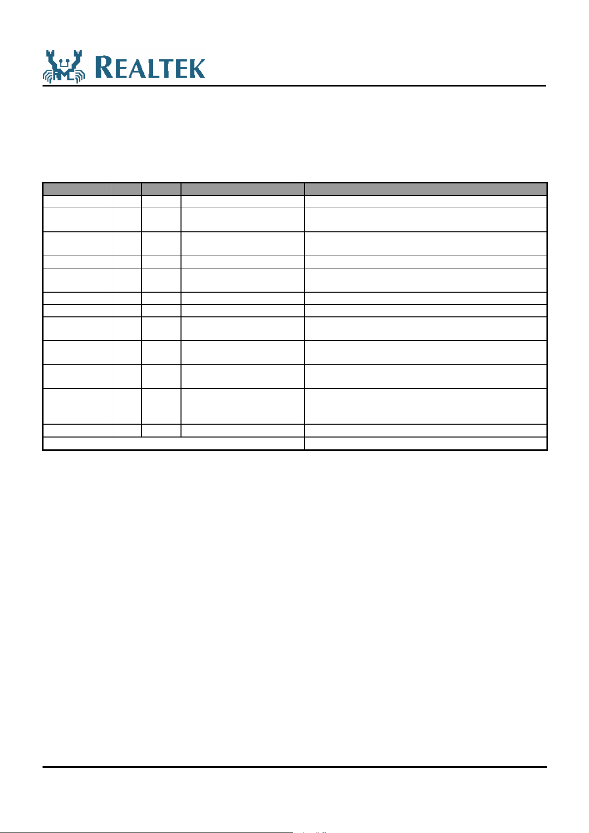
6.1 Mixer Registers
Access to registers with an odd number will return a 0. Reading unimplemented registers will also return a 0. X=Reserved bit.
REG.
(HEX)
00h Reset X SE4 SE3 SE2 SE1 SE0 ID9 ID8 ID7 ID6 ID5 ID4 ID3 ID2 ID1 ID0 0190h
02h Master
04h Headphone
06h Mono-Out
0Ah PC_BEEP
0Ch PHONE
0Eh MIC Volume Mute X X X X X BGO1 BGO0 X BC X MI4 MI3 MI2 MI1 MI0 8008h
10h Line-In
12h CD Volume Mute X X CL4 CL3 CL2 CL1 CL0 RM* X X CR4 CR3 CR2 CR1 CR0 8808h
16h Aux Volume Mute X X AL4 AL3 AL2 AL1 AL0 RM* X X AR4 AR3 AR2 AR1 AR0 8808h
18h PCM Out
1Ah Record Select X X X X X LRS2 LRS1 LRS0 X X X X X RRS2 RRS1 RRS0 0000h
1Ch ADC
1Eh MIC ADC
20h General
22h 3D Control X X X X X X X X X X X X X DP2 DP1 DP0 0000h
24h Audio Int. &
26h Power Down
28h Extended
2Ah Extended
2Ch PCM front Out
32h PCM Input
34h MIC Input
3Ah S/PDIF Ctl V DRS SPSR1 SPSR0 L CC6 CC5 CC4 CC3 CC2 CC1 CC0 PRE COPY /AUD
60h/
6Eh
76h GPIO Setup 0 0 0 0 0 0 0 0 0 0 0 0 0 0 0 0 0000h
78h GPIO Status 0 0 0 0 0 0 0 0 0 0 0 0 0 0 0 0 0000h
7Ch Vendor ID1 F7 F6 F5 F4 F3 F2 F1 F0 S7 S6 S5 S4 S3 S2 S1 S0 414Ch
7Eh Vendor ID2 T7 T6 T5 T4 T3 T2 T1 T0 DEV7 DEV6 DEV5 DEV4 DEV3 DEV2 DEV1 DEV0 4770h
NAME D15 D14 D13 D12 D11 D10 D9 D8 D7 D6 D5 D4 D3 D2 D1 D0
Volume
volume
Volume
Volume
Volume
Volume
Volume
Record Gain
Record Gain
Purpose
Paging
Ctrl/Status
Audio ID
Audio Status
Sample Rate
Sample Rate
Sample Rate
Vendor Define 0 0 0 0 0 0 0 0 0 0 0 0 0 0 0 0 0000h
Mute X ML5 ML4 ML3 ML2 ML1 ML0 RM* X MR5 MR4 MR3 MR2 MR1 MR0 8000h
Mute X HPL5 HPL4 HPL3 HPL2 HPL1 HPL0 RM* X HPR5 HPR4 HPR3 HPR2 HPR1 HPR0 8000h
Mute X X X X X X X X X X MM4 MM3 MM2 MM1 MM0 8000h
Mute X X F7 F6 F5 F4 F3 F2 F1 F0 PB3 PB2 PB1 PB0 X 8000h
Mute X X X X X X X X X X PH4 PH3 PH2 PH1 PH0 8008h
Mute X X NL4 NL3 NL2 NL1 NL0 RM* X X NR4 NR3 NR2 NR1 NR0 8808h
Mute X X PL4 PL3 PL2 PL1 PL0 RM* X X PR4 PR3 PR2 PR1 PR0 8808h
Mute X X X LRG3 LRG2 LRG1 LRG0 X X X X RRG3 RRG2 RRG1 RRG0 8000h
Mute X X X LMR
POP X 3D X DRSS1 DRSS0 MIX MS LBK X X X X X X X 0400h
I4 I3 I2 I1 I0 X X X X X X X PG3 PG2 PG1 PG0 0000h
EAPD PR6 PR5 PR4 PR3 PR2 PR1 PR0 X X X X REF ANL DAC ADC 000Fh
ID1 ID0 X X REV1 REV0 AMAP X X X X X X SPDIF DRA VRA 0A07h
X X X X X SPCV X X X X SPSA1 SPSA0 X SPDIF DRA VRA 0000h
FSR
FSR14 FSR13 FSR12 FSR11 FSR10 FSR9 FSR8 FSR7 FSR6 FSR5 FSR4 FSR3 FSR2 FSR1 FSR0 BB80h
15
ISR
ISR
ISR
15
MSR
15
14
MSR
14
13
MSR
13
ISR
12
MSR
12
G3
ISR
11
MSR
11
LMR
LMR
LMR
G2
G1
ISR
ISR 9 ISR 8 ISR 7 ISR 6 ISR 5 ISR 4 ISR 3 ISR 2 ISR 1 ISR 0 BB80h
10
MSR
MSR9 MSR8 MSR7 MSR6 MSR5 MSR4 MSR 3 MSR 2 MSR 1 MSR0 BB80h
10
X X X X RMR
G0
G3
RMR
G2
RMR
G1
IO
DEFAUL
T
RMR
8000h
G0
PRO 2000h
Two-Channel AC’97 2.3 Audio Codec Rev1.6
7
Page 12
ALC203 DataSheet
6.1.1 MX00 Reset
Default: 0190h
Writing any value to this register will start a register reset, and causes all of the registers to revert to their default values, then the
written data is ignored. Reading this register returns the ID code of the specific part.
Bit Type Function
15
14:10 R Return 00000b
9 R Read as 0 (No support for 20-bit ADC)
8 R Read as 1 (Support for 18-bit ADC)
7 R Read as 1 (Support for 20-bit DAC)
6 R Read as 0 (No support for 18-bit DAC)
5 R Read as 0 (No support for Loudness)
4 R Read as 1 (Headphone output support)
3 R Read as 0 (No simulated stereo; for analog 3D block use)
2 R Read as 0 (No Bass & Treble Control)
1 R
0 R Read as 0 (No dedicated MIC PCM input)
Reserved
Reserved, Read as 0
6.1.2 MX02 Master Volume
Default: 8000h
These registers control the overall volume level of the output functions. Each step on the left and right channels corresponds to
a 1.5dB increase/decrease in volume.
Bit Type Function
15 R/W
14
13:8 R/W
7:6
5:0 R/W
n For MRV/MLV: 00h 0 dB attenuation
3Fh 94.5 dB attenuation
Mute Control 0: Normal 1: Mute (-∞ dB)
Reserved
Master Left Volume (MLV[5:0]) in 1.5 dB steps
Reserved
Master Right Volume (MRV[5:0]) in 1.5 dB steps
6.1.3 MX04 Headphone
Default: 8000h
Register 04h controls the headphone (ALC203) output volume. Each step in bits 5:0 and 13:8 corresponds to a 1.5dB
increase/decrease in volume, allowing 63 levels of volume, from 000000 to 111111.
Bit Type Function
15 R/W
14
13:8 R/W
7:6
5:0 R/W
n For HPR/HPL: 00h 0 dB attenuation
3Fh 94.5 dB attenuation
Mute Control 0: Normal 1: Mute (-∞ dB)
Reserved
Headphone/True Line Output Left Volume (HPL[5:0]) in 1.5 dB steps
Reserved
Headphone/True Line Output Right Volume (HPR[5:0]) in 1.5 dB steps
Two-Channel AC’97 2.3 Audio Codec Rev1.6
8
Page 13
ALC203 DataSheet
6.1.4 MX06 MONO_OUT Volume
Default: 8000h
Register 06h controls the mono volume output. Mono output is the same data sent on all output channels. Each step in bits 4:0
corresponds to a 1.5dB increase/decrease in volume, allowing 32 levels of volume from 00000 to 11111.
Bit Type Function
15 R/W
14:5
4:0 R/W
n For MMV: 00h 0 dB attenuation
1Fh 46.5 dB attenuation
Mute Control 0: Normal 1: Mute (-∞ dB)
Reserved
Mono Master Volume (MMV[4:0]) in 1.5 dB steps
6.1.5 MX0A PC BEEP Volume
Default: 8000h
This register controls the input volume for the PC beep signal. Each step in bits 4:1 corresponds to a 3dB increase/decrease in
volume. 16 levels of volume are available, from 0000 to 1111.
The purpose of this register is to allow the PC Beep signals to pass through the ALC203, eliminating the need for an external system
speaker/buzzer. The PC BEEP pin is directly routed (internally hardwired) to the LINE-OUTL & R pins. If the PC speaker/buzzer is
eliminated, it is recommended to connect the external speakers at all times so the POST codes can be heard during reset.
Bit Type Function
15 R/W
14:13
12:5 R/W
4:1 R/W
0
n For PBV: 00h 0 dB attenuation
0Fh 45 dB attenuation
Mute Control 0: Normal 1: Mute (-∞ dB)
Reserved
Internal PCBEEP Frequency, F[7:0]
The internal PCBEEP frequency is the result of dividing the 48KHz clock by 4 times the number specified
in F[7:0].
The lowest tone is 48KHz/(255*4)=47Hz.
The highest tone is 48KHz/(1*4)=12KHz.
A value of 00h in F[7:0] disables internal PCBEEP generator and allows external PCBEEP input.
PC Beep Volume (PBV[3:0]) in 3 dB steps
Reserved
6.1.6 MX0C PHONE Volume
Default: 8008h
Register 0Ch controls the telephone input volume for software modem applications. Because software modem applications may
not have a speaker, the CODEC can offer a speaker-out service. Each step in bits 4:0 corresponds to a 1.5dB increase/decrease in
volume, allowing 32 levels of volume, from 00000 to 11111.
Bit Type Function
15 R/W
14:5
4:0 R/W
n For PV: 00h +12 dB Gain
08h 0dB gain
1Fh -34.5dB Gain
Two-Channel AC’97 2.3 Audio Codec Rev1.6
Mute Control 0: Normal 1: Mute (-∞ dB)
Reserved
Phone Volume (PV[4:0]) in 1.5 dB steps
9
Page 14
ALC203 DataSheet
6.1.7 MX0E MIC Volume
Default: 8008h
Register 0Eh controls the microphone input volume. Each step in bits 4:0 corresponds to a 1.5dB increase/decrease in volume,
allowing 32 levels of volume, from 00000 to 11111. Bit 6 enables/disables a boost in volume to a magnification based on bits 9:8.
Bit Type Function
15 R/W
14:10
9:8 R/W
7
6 R/W
5
4:0 R/W
n For MV: 00h +12 dB Gain
08h 0dB gain
1Fh -34.5dB Gain
o If 29.5dB boost gain is selected, input resistor can be reduced to save area of feedback resistor.
Mute Control 0: Normal 1: Mute (-∞ dB)
Reserved
Boost Gain Option (BGO)
00: 20 dB 01: 6 dB 10: 12 dB 11: 29.5 dB (V=30*Vmic-in)
Reserved
Boost Control (BC)
0: Disable 1: Enable Boost
Reserved
Mic Volume (MV[4:0]) in 1.5 dB steps
6.1.8 MX10 LINE_IN Volume
Default: 8808h
Register 10h controls the LINE_IN input volume. Each step in bits 4:0 corresponds to a 1.5dB increase/decrease in volume for
the right channel, allowing 32 levels of volume, from 00000 to 11111. Each step in bits 12:8 corresponds to a 1.5dB
increase/decrease in volume for the left channel, allowing 32 levels of volume, from 00000 to 11111.
Bit Type Function
15 R/W
14:13
12:8 R/W
7:5
4:0 R/W
n For NLV/NRV: 00h +12 dB Gain
08h 0dB gain
1Fh -34.5dB Gain
Mute Control 0: Normal 1: Mute (-∞ dB)
Reserved
Line-In Left Volume (NLV[4:0]) in 1.5 dB steps
Reserved
Line-In Right Volume (NRV[4:0]) in 1.5 dB steps
6.1.9 MX12 CD Volume
Default: 8808h
Register 12h controls the CD input volume. Each step in bits 4:0 corresponds to a 1.5dB increase/decrease in volume for the right
channel, allowing 32 levels of volume, from 00000 to 11111. Each step in bits 12:8 corresponds to a 1.5dB increase/decrease in
volume for the left channel, allowing 32 levels of volume, from 00000 to 11111.
Bit Type Function
15 R/W
14:13
12:8 R/W
7:5
4:0 R/W
n For CLV/CRV: 00h +12 dB Gain
08h 0dB gain
1Fh -34.5dB Gain
Mute Control 0: Normal 1: Mute (-∞ dB)
Reserved
CD Left Volume (CLV[4:0]) in 1.5 dB steps
Reserved
CD Right Volume (CRV[4:0]) in 1.5 dB steps
Two-Channel AC’97 2.3 Audio Codec Rev1.6
10
Page 15
ALC203 DataSheet
6.1.10 MX16 AUX Volume
Default: 8808h
Register 16h controls the auxiliary input volume. Each step in bits 4:0 corresponds to a 1.5dB increase/decrease in volume for
the right channel, allowing 32 levels of volume, from 00000 to 11111. Each step in bits 12:8 corresponds to a 1.5dB
increase/decrease in volume for the left channel, allowing 32 levels of volume, from 00000 to 11111.
Bit Type Function
15 R/W
14:13
12:8 R/W
7:5
4:0 R/W
n For ALV/ARV: 00h +12 dB Gain
08h 0dB gain
1Fh -34.5dB Gain
Mute Control 0: Normal 1: Mute (-∞ dB)
Reserved
AUX Left Volume (ALV[4:0]) in 1.5 dB steps
Reserved
AUX Right Volume (ARV[4:0]) in 1.5 dB steps
6.1.11 MX18 PCM_OUT Volume
Default: 8808h
Register 18h controls the PCM_OUT output volume. Each step in bits 4:0 corresponds to a 1.5dB increase/decrease in volume
for the right channel, allowing 32 levels of volume, from 00000 to 11111. Each step in bits 12:8 corresponds to a 1.5dB
increase/decrease in volume for the left channel, allowing 32 levels of volume, from 00000 to 11111.
Bit Type Function
15 R/W
14:13
12:8 R/W
7:5
4:0 R/W
n For PLV/PRV: 00h +12 dB Gain
08h 0dB gain
1Fh -34.5dB Gain
Mute Control 0: Normal 1: Mute (-∞ dB)
Reserved
PCM Volume (PLV[4:0]) in 1.5 dB steps
Reserved
PCM Right Volume (PRV[4:0]) in 1.5 dB steps
Two-Channel AC’97 2.3 Audio Codec Rev1.6
11
Page 16
ALC203 DataSheet
6.1.12 MX1A Record Select
Default: 0000h
Register 1Ah controls the record input source. Each bit in bits 2:0 selects a recording source for the right channel. Each bit in bits
10:8 selects a recording source for the left channel.
Bit Type Function
15:11
10:8 R/W
7:3
2:0 R/W
n For LRS
o For RRS
Reserved
Left Record Source Select (LRS[2:0])
Reserved
Right Record Source Select (RRS[2:0])
0 MIC
1 CD LEFT
2 Muted
3 AUX LEFT
4 LINE LEFT
5 STEREO MIXER OUTPUT LEFT
6 MONO MIXER OUTPUT
7 PHONE
0 MIC
1 CD RIGHT
2 Muted
3 AUX RIGHT
4 LINE RIGHT
5 STEREO MIXER OUTPUT RIGHT
6 MONO MIXER OUTPUT
7 PHONE
6.1.13 MX1C Record Gain for Stereo ADC
Default: 8000h
Register 1Ch controls the record gain. Each step in bits 3:0 corresponds to a 1.5dB increase/decrease in gain for the right
channel, allowing 16 levels of gain, from 0000 to 1111. Each step in bits 11:8 corresponds to a 1.5dB increase/decrease in gain
for the left channel, allowing 16 levels of gain, from 0000 to 1111.
Bit Type Function
15 R/W
14:12
11:8 R/W
7:4
3:0 R/W
nFor LRG/RRG: 0Fh +22.5dB
Mute Control 0: Normal 1: Mute (-∞ dB)
Reserved
Left Record Gain Select (LRG[3:0]) in 1.5 dB steps
Reserved
Right Record Gain Select (RRG[3:0]) in 1.5 dB steps
00h 0 dB (No Gain)
Two-Channel AC’97 2.3 Audio Codec Rev1.6
12
Page 17

ALC203 DataSheet
6.1.14 MX1E Record Gain for MIC ADC
Default: 8000h
Register 1Eh controls the record gain. Each step in bits 3:0 corresponds to a 1.5dB increase/decrease in gain for the right
channel, allowing 16 levels of gain, from 0000 to 1111. Each step in bits 11:8 corresponds to a 1.5dB increase/decrease in gain
for the left channel, allowing 16 levels of gain, from 0000 to 1111.
Bit Type Function
15 R/W
14:12
11:8 R/W
7:4
3:0 R/W
nFor LRG/RRG: 0Fh +22.5dB
Mute Control 0: Normal 1: Mute (-∞ dB)
Reserved
Left Record Gain Select (LMRG[3:0]) in 1.5 dB steps
Reserved
Right Record Gain Select (RMRG[3:0]) in 1.5 dB steps
00h 0 dB (No Gain)
6.1.15 MX20 General Purpose Register
Default: 0000h
This register is used to control several functions. Bit 13 enables or disables 3D control. Bit 9 allows selection of mono output. Bit
8 controls the MIC selector. Bit 7 enables loopback of the AD output to the DA input without involving the AC-Link, allowing
for full system performance measurements.
Bit Type Function
15:14
13 R/W
12:9
8 R/W
7 R/W
6:0
Reserved, Read as 0
3D Control 1: On 0: Off
Reserved, Read as 0
MIC Select 0: MIC 1 1: MIC 2
AD to DA Loop-back Control 0: Disable 1: Enable
Reserved
6.1.16 MX22 3D Control
Default: 0000h
This register is used to control the 3D stereo enhancement function built into the AC’97 component. The register bits, DP2-DP0
are used to control the separation ratios in the 3D control for both LINE_OUT and DAC_OUT.
The 3D stereo enhancement function provides for a deeper and wider sound experience with a potential 6-speaker arrangement.
Note that the 3D bit in the general purpose register (bit 13) must be set to 1 to enable this function.
Bit Type Function
15:3
2:0 R/W
n3D effect control
DP[2:0] Function DP[2:0] Function
Reserved, Read as 0
Depth Control (DP[2:0])
000 0% (off*) 100 50%
001 12.5% 101 67.5%
010 25% 110 75%
011 37.5 111 100%
Two-Channel AC’97 2.3 Audio Codec Rev1.6
13
Page 18

ALC203 DataSheet
6.1.17 MX24 Audio interrupt and Paging
Default: 0000h
Bit Type Function
15
14 R
13 R
12 R/W
11 R/W
10:4 NA Reserved, read as 0
3:0 R/W
Interrupt Status, I4
0: Interrupt is clear
1: Interrupt was generated
Interrupt event and status are clear by writing a 1 to this bit. The status will change regardless of interrupt
enable (I0).
Interrupt Cause, I3
I3=0: GPIO, SPDIF-IN and Jack-Detect interrupt status in MX78 are not changed.
1: GPIO, SPDIF-IN and Jack-Detect interrupt status in MX78 are changed.
I3= (MX78.14|MX78.13|MX78.12|MX78.6|MX78.5|MX78.4)
This bit reflects the cause of the first interrupt event generated. Software should read it after interrupt
status (I4) has been confirmed as interrupting. I3 will be zero when I4 is cleared.
Interrupt Cause, I2
I2=0: Sense value in page ID-01h MX6A.[12:8] has not changed.
1: Sense cycle completed or new sense value in page ID-01h MX6A.[12:8] is available.
This bit reflects the cause of the first interrupt event generated. Software should read it after interrupt
status (I4) has been confirmed as interrupting. I2 will be zero when I4 is cleared.
Sense Cycle, I1
0: Sense cycle not in progress
1: Sense cycle start
Writing a ‘1’ to this bit causes a sense cycle start. If a sense cycle is in progress, writing a ‘0’ to this bit will
abort the sense cycle.
Whether the data in the sense result register (page ID-01h MX6A) is valid or not is determined by the IV
bit in MX6A, Page ID-1h.
Interrupt Enable, I0
0: Interrupt is masked, interrupt status (I4) will not be shown in bit 0 in Slot 12 in SDATA-IN.
1: Interrupt is un-masked, interrupt status (I4) will be shown in bit 0 in Slot 12 in SDATA-IN.
Page Selector, PG[3:0]
0000b: Vendor Specific
0001b: Page ID 01 (AC’97 2.3 Discovery Descriptor Definition)
Others: Reserved.
This register is used to select a descriptor of 16 word pages between registers MX60 to MX6F. Value of 0
is used to select vendor specific space to maintain compatibility with AC’97 2.2 vendor specific register.
Once PG[3:0] is not 0000b and 0001b, ALC203 will return zero data for ACLINK mixer read command.
Two-Channel AC’97 2.3 Audio Codec Rev1.6
14
Page 19

ALC203 DataSheet
6.1.18 MX26 Powerdown Control/Status
Default: 000Fh
This read/write register is used to program power-down states and monitor subsystem readiness. The lower half of this register is
read only status; a “1” indicating that the subsection is “ready.” Ready is defined as the subsection’s ability to perform in its nominal
state. When this register is written, the bit values that come in on AC-Link will have no effect on read only bits 0-7 and bit 15.
When the AC-Link “CODEC Ready” indicator bit (SDATA_IN slot 0, bit 15) is a 1, it indicates that the AC-Link and AC’97
control and status registers are in a fully operational state. The AC’97 controller must further probe this powerdown control
/status register to determine exactly which subsections, if any, are ready.
Bit Type Function
15 R/W
14 R/W
13 R/W
12 R/W
11 R/W
10 R/W
9 R/W
8 R/W
7:4
3 R
2 R
1 R
0 R
nTruth table for power down mode :
ADC DAC Mixer Verf ACLINK Int CLK HP-OUT EAPD
PR0=1 PD
PR1=1 PD
PR2=1 PD PD
PR3=1 PD PD PD PD PD
PR4=1 PD PD PD
PR5=1 PD PD PD
PR6=1 PD
PR7=1 PD
PD: Power down Blank: Don’t care
oIf Mixer is power down (PR2=1 or PR3=1), the LINE-OUT (pin-35/36) is shut down and its output is floated.
pIf Headphone-Out is power down (PR6=1), the HP-OUT (pin-39/41) is shut down and its output is floated.
PR7 External Amplifier Power Down (EAPD) 0: Normal 1: Power down
PR6 0: Normal 1: Power down Headphone Out (HP-OUT, pin-39/41)
PR5 0: Normal 1: Disable internal clock
PR4 0: Normal 1: Power down AC-Link
PR3 0: Normal 1: Power down Mixer (Vref off)
PR2 0: Normal 1: Power down Mixer (Vref still on)
PR1 0: Normal 1: Power down PCM DAC
PR0 0: Normal 1: Power down PCM ADC and input MUX
Reserved, Read as 0
Vref Status 1: Vref is up to normal level 0: Not yet ready
Analog Mixer Status 1: Ready 0: Not yet ready
DAC Status 1: Ready 0: Not yet ready
ADC Status 1: Ready 0: Not yet ready
Two-Channel AC’97 2.3 Audio Codec Rev1.6
15
Page 20

ALC203 DataSheet
6.1.19 MX28 Extended Audio ID
Default: 0605h
The Extended Audio ID register is a read only register used to communicate information to the digital controller on two functions. ID1
and ID0 echo the configuration of the CODEC as defined by the programming of pins 45 and 46 externally. “00” returned defines the
CODEC as the primary CODEC, while any other code identifies the CODEC as one of three secondary CODEC possibilities.
Bit Type Function
15 R
14 R
13:12
11:10 R REV[1:0]=10 to indicate that the ALC203 is AC’97 rev2.3 compliant
9 R
8:6
5:4 R/W
3
2 R
1 R
0 R
n ID[1:0] depend on the states of pins 46, 45, 44, and 43 when power-on reset or AC97_RESET# is active. Refer to
section 9.1 for detailed information on configuration of ID[1:0].
o The ALC203 maps DAC slot according to the following table: (default maps to AC’97 spec. rev2.3)
ID1
ID0
Reserved, Read as 0
AMAP read as 1 (DAC mapping based on ID)
Reserved, Read as 0
DAC Slot Assignment DSA[1:0] (Default value depends on ID[1:0])
DSA[1:0] Controls the DAC slot assignment, as described in AC’97 rev2.2.
Reserved, Read as 0
SPDIF Read as 1 (S/PDIF is supported)
DRA Read as 1
VRA Read as 1 (Variable Rate Audio is supported)
DSA[1:0]
0,0 3 4 Default when ID[1:0]=00
0,1 7 8 Default when ID[1:0]=01,10
1,0 6 9 Default when ID[1:0]=11
1,1 10 11 -
Left DAC slot # Right DAC slot # Comment
Two-Channel AC’97 2.3 Audio Codec Rev1.6
16
Page 21

ALC203 DataSheet
6.1.20 MX2A Extended Audio Status and Control,
Default: 0000h
This register contains two active bits for power-down and status of the surrounding DACs. Bits 0, 1, and 2 are read/write bits
which are used to enable or disable VRA, DRA, and SPDIF respectively. Bits 4 and 5 are read/write bits used to determine the
AC-LINK slot assignment of the S/PDIF. Bit 10 is a read-only bit which tells the controller if the S/PDIF configuration is valid.
Bit Type Function
15 R/W
14:11 NA
10 R
9:6
5:4 R/W
3
2 R/W
1 R/W
0 R/W
n If VRA = 0, the ALC203’s ADC/DAC operate at a fixed 48KHz sampling rate. Otherwise, they operate at a variable
sampling rate defined in MX2C and MX32. VRA also controls the write operation of MX2Cand MX32.
o DRA can be written when (ID=00)&(DSA=00), otherwise it is always 0.
If DRA = 1, DAC operates at a fixed 96KHz sampling rate. The PCM(n) and PCM(n+1) data is captured in the same
frame. In this mode, MX2C is fixed at BB80h, MX32 and ADC is still controlled by VRA.
pSPCV is a read-only bit that indicates whether the current S/PDIF-Out configuration is supported or not. If the
configuration is supported, SPCV is set as 1 by H/W. So driver can check this bit to determine the status of the
S/PDIF transmitter system. SPCV is always operating, independent of the SPDIF enable bit (MX2A.2). The
S/PDIF output is active if MX2A.2 is set in spite of SPCV. Once S/PDIF output is enabled but SPCV is invalid
(SPCV=0), channel status is still output, but the output data bits will be all zero.
Validity Configuration of S/PDIF Output (VCFG)
Combines with MX3A.15 to decide validity control in S/PDIF output signal.
Reserved
S/PDIF Configuration Valid (SPCV)
0: Current S/PDIF configuration {SPSA, SPSR,DAC/slot rate} is not valid.
1: Current S/PDIF configuration {SPSA, SPSR,DAC/slot rate} is valid.
Reserved
SPSA[1:0], S/PDIF Slot Assignment when DRS=0
00: S/PDIF source data assigned to AC-LINK slot3/4
01: S/PDIF source data assigned to AC-LINK slot7/8 (Default when ID=00)
10: S/PDIF source data assigned to AC-LINK slot6/9 (Default when ID=01,10)
11: S/PDIF source data assigned to AC-LINK slot10/11 (Default when ID=11)
SPSA[1:0], S/PDIF-Out Slot Assignment when DRS=1(for 96K S/PDIF-Out)
01: S/PDIF-Out source is from AC-LINK slot 3/4 + slot 7/8.
Reserved
SPDIF 1: Enable 0: Disable (SPDIFO is in high impedance)
DRA 1: Enable 0: Disable
VRA 1: Enable 0: Disable
Two-Channel AC’97 2.3 Audio Codec Rev1.6
17
Page 22

ALC203 DataSheet
6.1.21 MX2C PCM DAC Rate
Default: BB80h
The ALC203 allows adjustment of the output sample rate. This register is used to adjust the sample rate. By changing the values,
sampling rates from 8000 to 48000 can be chosen.
Bit Type Function
15:0 R/W
n The ALC203 supports the following sampling rates, as required in the PC99/PC2001 design guide.
oNote that If the value written is not support, the closest value is returned.
When MX2A.0=0 (VRA is disable), this register will return BB80h when read.
Output Sampling Rate FOSR[15:0]
Sampling rate FOSR[15:0]
8000 1F40h
11025 2B11h
12000 2EE0
16000 3E80h
22050 5622h
24000 5DC0
32000 7D00h
44100 AC44h
48000 BB80h
6.1.22 MX32 PCM ADC Rate
Default: BB80h
The ALC203 allows adjustment of the input sample rate. This register is used to adjust the sample rate. By changing the values,
sampling rates from 8000 to 48000 can be chosen.
Bit Type Function
15:0 R/W
n The ALC203 supports the following sampling rates, as required in the PC99/PC2001 design guide.
oNote that if the value written is not supported, the closest value is returned.
When MX2A.0=0 (VRA is disable), this register will return BB80h when read.
Output Sampling Rate FISR[15:0]
Sampling rate FISR[15:0]
8000 1F40h
11025 2B11h
12000 2EE0
16000 3E80h
22050 5622h
24000 5DC0
32000 7D00h
44100 AC44h
48000 BB80h
Two-Channel AC’97 2.3 Audio Codec Rev1.6
18
Page 23

s
ALC203 DataSheet
6.1.23 MX3A S/PDIF Out Channel Status/Control
Default: 2000h
Bit Type Function
15 R/W
14 R
13:12 R/W
11 R/W
10:4 R/W
3 R/W
2 R/W
1 R/W
0 R
nThe consumer channel status block (bit0~bit31):
PRO=0 /AUDIO COPY PRE 0 0 0 0
o The “V” bit in the sub-frame is determined by Validity control (MX3A.15) and VCFG (MX2A.15):
Validity VCFG Operation
Validity Control (control V bit in Sub-Frame)
0: The V bit (valid flag) in the sub-frame depends on whether the S/PDIF data is under-run or over-run.
1: The V bit in sub-frame is always sent as 1 to indicate the invalid data is not
suitable for receiver.
DRS (Double Rate S/PDIF)
0: 32K, 44.1K, 48K S/PDIF-Out
1: 96K S/PDIF-Out
This bit can only be set when SPSR is 10b.
S/PDIF Sample Rate SPSR[1:0]
00: Sample rate set to 44.1KHz, Fs[0:3]=0000
01: Reserved
10: Sample rate set to 48.0KHz, Fs[0:3]=0100 (default)
11: Sample rate set to 32.0KHz, Fs[0:3]=1100
Generation Level (LEVEL)
Category Code (CC[6:0])
Preemphasis (PRE)
0: None 1: Filter pre-emphasis is 50/15 µsec
Copyright (COPY)
0: Not asserted 1: Asserted
Non-Audio Data type (/AUDIO)
0: PCM data 1: AC3 or other digital non-audio data
Professional or Consumer format (PRO)
0: Consumer format 1: Professional format
The ALC203 supports consumer channel status format, so this bit is always 0.
0 1 2 3 4 5 6 7
8 9 10 11 12 13 14 15
CC0 CC1 CC2 CC3 CC4 CC5 CC6 LEVEL
16 17 18 19 20 21 22 23
0 0 0 0 0 0 0 0
24 25 26 27 28 29 30 31
Fs0 Fs1 Fs2 Fs3 0 0 0 0
0 0 If S/PDIF FIFO is under-run, the “V” bit in the sub-frame is set to
indicate that the S/PDIF data is invalid.
0 1 If S/PDIF FIFO is under-run, the “V” bit in the sub-frame is alway
0, and pads the data with “0”s.
1 0 The “V” bit is always 1, and data bits (bit 8 ~ bit 27) should be
forced to 0.
1 1 The “V” bit in sub-frame is always “0”, and the S/PDIF output data
should be forced to zero.
Two-Channel AC’97 2.3 Audio Codec Rev1.6
19
Page 24

ALC203 DataSheet
6.2 Vendor Defined Registers (Page-00h)
These registers are available to Realtek and Realtek customers for specialized functions.
6.2.1 Page -0h, MX60 S/PDIF In Status [15:0]
Default: 0000h
The data in MX60 are captured from channel status [15:0] of S/PDIF-IN signal.
Bit Type Function
15 R LEVEL (Generation Level)
14:8 R CC[6:0] (Category Code)
7:6 R Mode[1:0]
5:3 R PRE[2:0] (Pre-Emphasis)
2 R COPY (Copyright)
0: asserted 1: Not asserted
1 R /AUDIO (Non-Audio Data type)
0: PCM data 1: AC3 or other digital non-audio data
0 R PRO (Professional or Consumer format)
0: consumer format 1: professional format
6.2.2 Page -0h, MX62 S/PDIF In Status [29:15]
Default: 0000h
The data in MX62 are captured from channel status [29:16] of S/PDIF-IN signal.
Bit Type Function
15 R “V” bit in sub-frame of SPDIFI
0: Data X and Y are valid
1: At least one of data X and Y is invalid
This bit is real-time updated, and it is meaning when S/PDIF-IN is locked
14 R S/PDIF-IN Input Signal Locked by hardware
0: Unlocked 1: Locked
13:12 R Ca[1:0] ( Clock Accuracy)
11:8 R Fs[3:0]. (Sample Frequency in channel status)
0000: 44.1KHz
0010: 48 KHz
0011: 32 KHz
Others: Reserved
7:4 R Cn[3:0] (Channel Number)
3:0 R Sn[3:0] (Source Number)
6.2.3 Page -0h, MX6A Data Flow Control
Default: 0000h
Bit Type Function
15 NA Reserved
14 R/W
13:12 R/W
11 R/W
Direct DAC Mode
0: Analog output is from summation of DAC and analog inputs.
1: Analog output is from DAC.
S/PDIF Out Source
00:S/PDIF data is from ACLINK controller
01: Reserved.
10:Directly bypass S/PDIF-In signal to S/PDIF-Out.
11: Reserved.
Recorded PCM Data to ACLINK
Two-Channel AC’97 2.3 Audio Codec Rev1.6
20
Page 25

ALC203 DataSheet
Bit Type Function
0: Recorded PCM data to host is from original ADC
1: Recorded PCM data to host is from S/PDIF-IN
10:8 NA Reserved
7 R/W
6 R/W
5:2 NA Reserved
1 R/W
0 R/W
MIC2 Source
0: MIC2 1: (MIC1+MIC2)/2.
ADC MIC Source
0: Mono duplicated. (Default) 1: Stereo.
S/PDIF-In Enable
0: Disable
1: Enable
S/PDIF-In Monitoring Control
0: Disable, SPDIFI data is not added into PCM data to DAC. (Default)
1: Enable, SPDIFI data will be added into PCM data to DAC after SPDIFI is locked.
6.3 Discovery Descriptor (Page ID-01h)
These registers are defined in Ac’97 2.3 for sensing and analog plug & play functions.
6.3.1 Page -1h, MX62 PCI Sub System ID
Default: FFFFh
Bit Type Function
15:0 R/W
PCI Sub System Vendor ID
This register can be written once only after power on, and is not affected by AC97 cold reset. The system
manufacture’s BIOS can set its own sub-system ID.
The default value FFFFh means this register is implemented and data is not set by BIOS.
6.3.2 Page -1h, MX64 PCI Sub Vendor ID
Default: FFFFh
Bit Type Function
15:0 R/W
PCI Vendor ID
This register can be written once only after power on, and is not affected by AC97 cold reset. The system
manufacture’s BIOS can set its own sub-vendor ID.
The default value FFFFh means this register is implemented and data is not set by BIOS.
Two-Channel AC’97 2.3 Audio Codec Rev1.6
21
Page 26

ALC203 DataSheet
6.3.3 Page -1h, MX66 Sense Function Select
Default: 0000h
Bit Type Function
15:5 Reserved
4:1 R/W
0 R/W
Function Code bits, FC[3:0]
These bits specify the type of audio function described in page ID-01h MX66, MX68 and MX6A.
0h: LINE OUT
1h: HP OUT
5h: MIC1 In
6h: MIC2 In
7h: LINE In
Others: Not supported
Tip or Ring Selection, T/R
This bit sets which jack conductor the sense value is measured from. It is combined with FC[3:0].
0: Tip (Left channel)
1: Ring (Right channel)
6.3.4 Page -1h, MX68 Sense Function
Default: 02F1h
Bit Type Function
15:11 R/W
10 R/W
9:5 R/W
4 R/W
3:1 NA Reserved
0 R
Gain bits, G[4:0]
These bits are updated by BIOS to tell driver the gain supported by external amplifier. 1 LSB = 1.5dBV
00000b: 0dBV, 00001b: +1.5dBV,… 01111b:+24dBV
10000b: 0dBV, 10001b: -1.5dBV,… 11111b: -24dBV
Inversion bit, INV
0: No inversion reported 1: Inverted.
Buffer delays, DL[4:0]
Delay measurement for the signal from inputs to outputs channels in 20.83µsec (1/48000 second) units.
Information Valid bit, IV
0: After a sense cycle is completed, indicates that no information is provided on the sensing method
1: After a sense cycle is completed, indicates that information is provided on the sensing method
Clearing this bit by writing “1”, writing “0” to this bit has no effect.
Function Information Present, FIP
This bit when set to a ‘1’ indicates that the G[4:0], INV, DL[4:0] and ST[2:0] bits are supported and are
Read/Write capable.
Two-Channel AC’97 2.3 Audio Codec Rev1.6
22
Page 27

ALC203 DataSheet
6.3.5 Page -1h, MX6A Sense Detail
Default: 0000h
Bit Type Function
15:13 R/W
12:8 R
7:0 R Always read as 0.
Connection/Jack Location bits, ST[2:0]
000b: Rear I/O Panel (Default)
001b: Front Panel
010b: Motherboard
011b: Dock/External
100b ~ 110b: Reserved
111b: Unused I/O.
These bits should be written by the BIOS to let the driver know where the specified I/O FC[3:0] are
located.
Sense bits, S[4:0] (Default value depends on sensed result after Cold Reset)
For output devices:
02h: Not specificed or unknown 05h: Powered speaker 06h: Earphone or passive speaker
Other: Not supported
For input deices:
12h: Not specified or unknown 13h: Mono Microphone 15h: Stereo Line-In
Other: Not supported
This field reports the type of output/input peripheral plugged in the jack after sensing.
Two-Channel AC’97 2.3 Audio Codec Rev1.6
23
Page 28

ALC203 DataSheet
6.4 Extension Registers
6.4.1 MX76 GPIO & Interrupt Setup
Default: 0000h
Bit Type Function
15 R/W
14 R/W
13 R/W
12 R/W
11:7 Reserved
6 R/W
5 R/W
4 R/W
3:2 Reserved
1 R/W
0 R/W
GPIO Status Indication in SDATA_IN
0:The status of GPIO0/GPIO1/JD and its valid tag are not indicated in SDATA_IN.
1: The status of GPIO0/GPIO1/JD and its valid tag are indicated in SDATA_IN
SPDIFI Valid Interrupt Enable
0:Disable 1: Enable
SPDIFI Lock Interrupt Enable
0:Disable 1: Enable
JD2 (Jack-Detect 2) interrupt Enable
0: Disable 1: Enable.
A low to high transaction will trigger the JD2 interrupt in bit0 of SDATA_IN’s slot-12.
JD1 (Jack-Detect 1) interrupt Enable
0: Disable 1: Enable.
A low to high transaction will trigger the JD interrupt in bit0 of SDATA_IN’s slot-12.
GPIO1 interrupt Enable (when GPIO1 is used as input)
0: Disable 1: Enable.
A low to high transaction will trigger the GPIO interrupt in bit0 of SDATA_IN’s slot-12.
GPIO0 interrupt Enable (when GPIO0 is used as input)
0: Disable 1: Enable.
A low to high transaction will trigger the GPIO interrupt in bit0 of SDATA_IN’s slot-12.
GPIO1Primitive Control
0: Set GPIO1 as input pin.
1: Set GPIO1 as output pin.
GPIO0 Primitive Control
0: Set GPIO0 as input pin.
1: Set GPIO0 as output pin.
Two-Channel AC’97 2.3 Audio Codec Rev1.6
24
Page 29

ALC203 DataSheet
6.4.2 MX78 GPIO & Interrupt Status
Default: 0000h
Bit Type Function
15 NA Reserved
14 R/W
13 R/W
12 R/W
11:10 NA Reserved
9 R/W
8 R/W
7 NA Reserved
6 R/W
5 R/W
4 R/W
3 NA Reserved
2 R
1 R
0 R
S/PDINF-In Valid Interrupt Status (SPDIFIN_VIS).
0: No SPDIFI Valid Interrupt.
1: SPDIFI Valid interrupt.
Write 1 to clear this status bit and its interrupt.
S/PDINF-In Lock Interrupt Status (SPDIFIN_LIS).
0: No SPDIFI Lock interrupt.
1: SPDIFI LOCK interrupt.
Write 1 to clear this status bit and its interrupt.
JD2 Interrupt Status (JD2_IS)
0: No JD2 interrupt.
1: JD2 interrupt.
Write 1 to clear this status bit.
GPIO1 Output Control
0: Drive GPIO1 low.
1: Drive GPIO1 high.
GPIO0 Output Control
0: Drive GPIO0 as low.
1: Drive GPIO0 as high.
JD1 Interrupt Status (JD1_IS)
0: No JD1 interrupt.
1: JD1 interrupt.
Write 1 to clear this status bit.
GPIO1 Interrupt Status (GPIO1_IS). (When GPIO1 is used as input)
0: No GPIO1 interrupt.
1: GPIO1 interrupt.
Write 1 to clear this status bit.
GPIO0 Interrupt Status (GPIO0_IS). (When GPIO0 is used as input)
0: No GPIO0 interrupt.
1: GPIO0 interrupt.
Write 1 to clear this status bit.
Jack-Detect Event (JDEVT)
0: No Jack-Detect event occurs.
1: Jack-Detect event occurs.
JDEVT = JDS1 | JDS2
Software can check this bit and MX7A.1 to know the status of JDx.
When MX7A.5=0, MX7A.1=JDS1.
When MX7A.5=1, MX7A.1=JDS2.
GPIO1 Input Status
0: GPIO1 is driven low by external device (input).
1: GPIO1 is driven high by external device (input).
GPIO0 Input Status
0: GPIO0 is driven low by external device (input).
1: GPIO0 is driven high by external device (input).
Two-Channel AC’97 2.3 Audio Codec Rev1.6
25
Page 30

ALC203 DataSheet
6.4.3 MX7A Miscellaneous Control
Default: 0000h
Bit Type Function
15:11 NA Reserved
10 R/W
9 R/W
8 R/W
7:6 NA Reserved
5 R/W
4 R/W
3 R/W
2 R/W
1 R
0 R/W
Pin-37 Function Selection (MONO-OUT or Vrefout3)
0: Vrefout3
1: MONO-OUT
Vrefout Off Control
0: Vrefout is normal on (output of buffered Vref).
1: Vrefout is off. (In High-Z).
Vrefout / Vrefout2 / Vrefout3 Level Control
0: 2.5V 1: 4.0V
Source of Jack-Detect status for MX7A.1
0: MX7A.1 indicates the status of Jack-Detect 1
1: MX7A.1 indicates the status of Jack-Detect 2
HP-OUT Control
0: Normal
1: HP-OUT is muted by H/W when MX7A.1=1
MONO-OUT Control
0: Normal
1: MONO-OUT is muted by H/W when MX7A.1=1
SPDIF Output Gating
0: SPDIF output is not gated with MX7A.1
1: SPDIF output is gated with MX7A.1. (SPDIFO is forced to 0 if MX7A.1=0)
Status of Jack-Detect 1 or 2 (JDSx)
0: JDSx is pull low
1: JDSx is floating or pull high
LINE-OUT Output Control
0: Normal
1: LINE-OUT output is muted by H/W when MX7A.1=1
6.4.4 MX7C Vendor ID1
The two registers (MX7C Vendor ID1 and MX7E Vendor ID2) contain four 8-bit ID codes. The first three codes have been
assigned by Microsoft for Plug and Play definitions. The fourth code is a Realtek assigned code identifying the ALC203. The
MX7C Vendor ID1 register contains the value 414Ch, which is the first and second characters of the Microsoft ID code. The
MX7C Vendor ID2 register contains the value 4770h, which is the third of the Microsoft ID code
Default: 414Ch
Bit Type Function
15:0 R
Vendor ID “AL”
6.4.5 MX7E Vendor ID2
Default: 4770h
Bit Type Function
15:8 R
7:0 R
Two-Channel AC’97 2.3 Audio Codec Rev1.6
Vendor ID - “G”
Device ID – 70h for ALC203
26
Page 31

ALC203 DataSheet
7. Electrical Characteristics
7.1 DC Characteristics
7.1.1 Absolute Maximum Ratings
Parameter Symbol Minimum Typical Maximum Units
Power Supplies
Digital
Analog
Operating Ambient Temperature Ta 0 - +70
Storage Temperature Ts +125
ESD (Electrostatic Discharge)
Susceptibility Voltage
Pin 9
Other Pins
Note ** : The standard testing condition before shipping is AVDD = 5.0V unless specified. Customers designing with a different
AVDD should contact Realtek technical support.
DVDD
AVDD**
3.0
3.3
3.3
5.0
4500 V
5000 V
3.6
5.5
o
o
V
V
C
C
7.1.2 Threshold Hold Voltage
Dvdd= 3.3V±5%, T
Parameter Symbol Minimum Typical Maximum Units
Input voltage range V
Low level input voltage
(XTLIN, SYNC, SDOUT, RESET#,
BITCLK, GPIO, S/PDIF-IN)
High level input voltage
(XTLIN, SYNC, SDOUT, RESET#,
BITCLK, GPIO, S/PDIF-IN)
High level output voltage V
Low level output voltage V
Input leakage current - -10 - 10 µA
Output leakage current
(Hi-Z)
Output buffer drive current - - 5 - mA
Internal pull up resistance - 30k 50k 100k
=250C, with 50pF external load.
ambient
in
V
IL
V
IH
OH
OL
- -10 - 10 µA
-0.30 - Dvdd+0.30 V
- - 0.5Dvdd V
0.5DVdd - - V
0.9DVdd - V
- - 0.1DVdd V
Ω
7.1.3 Digital Filter Characteristics
Filter Symbol Minimum Typical Maximum Units
ADC Lowpass Filter Passband 0 - 19.2 KHz
Stopband 28.8 KHz
Stopband Rejection -76.0 dB
Passband
Frequency Response
DAC Lowpass Filter Passband 0 - 19.2 KHz
Stopband 28.8 KHz
Stopband Rejection -78.5 dB
Passband
Frequency Response
+- 0.20 dB
+- 0.20 dB
Two-Channel AC’97 2.3 Audio Codec Rev1.6
27
Page 32

ALC203 DataSheet
7.1.4 S/PDIF output Characteristics
Dvdd= 3.3V, T
Parameter Symbol Minimum Typical Maximum Units
High level output voltage V
Low level output voltage V
=250C, with 75Ω external load.
ambient
OH
OL
7.2 AC Timing Characteristics
7.2.1 Cold Reset
Parameter Symbol Minimum Typical Maximum Units
RESET# active low pulse width T
RESET# inactive to BIT_CLK
Startup delay
RESET#
rst_low
T
rst2clk
162.8 - - ns
Trst_low
3.0 3.3 V
- 0 0.3 V
1.0 - - µs
Trst2clk
BITCLK
7.2.2 Warm Reset
Parameter Symbol Minimum Typical Maximum Units
SYNC active high pulse width T
SYNC inactive to BIT_CLK
Startup delay
SYNC
BITCLK
sync_high
T
sync2clk
Cold reset timing diagram
1.0 - - µs
162.8 - - ns
Tsync_high
Warm reset timing diagram
Tsync2clk
Two-Channel AC’97 2.3 Audio Codec Rev1.6
28
Page 33

ALC203 DataSheet
7.2.3 AC-Link Clocks
Parameter Symbol Minimum Typical Maximum Units
BIT_CLK frequency
BIT_CLK period T
BIT_CLK output jitter
BIT_CLK high pulse width (note 2) T
BIT_CLK low pulse width (note 2) T
SYNC frequency
SYNC period T
SYNC high pulse width T
SYNC low pulse width T
clk_period
clk_high
clk_low
sync_period
sync_high
sync_low
- 12.288 - MHz
- 81.4 - ns
- - 750 ps
36 40.7 45 ns
36 40.7 45 ns
- 48.0 - KHz
- 20.8 - µs
- 1.3 - µs
- 19.5 - µs
Note 1: Worse case duty cycle restricted to 45/55.
7.2.4 Data Output and Input Timing
Parameter Symbol Minimum Typical Maximum Units
Output Valid Delay from rising
edge of BIT_CLK
Note 1: Timing is for SDATA and SYNC outputs with respect to BIT_CLK at the device driving the output.
Note 2: 50pF external load
Parameter Symbol Minimum Typical Maximum Units
Input Setup to falling edge of
BIT_CLK
Input Hold from falling edge of
BIT_CLK
Note: Timing is for SDATA and SYNC outputs with respect to BIT_CLK at the device driving the output.
Parameter Symbol Minimum Typical Maximum Units
BIT_CLK combined rise or fall
plus flight time
SDATA combined rise or fall plus
flight time
Note: Combined rise or fall plus flight times are provided for worst case scenario modeling purposes.
t
t
setup
t
hold
co
- - 15 ns
10 - - ns
10 - - ns
- - 7 ns
- - 7 ns
TsetupThold
BITCLK
V
IL
SDATA-OUT
SDATA-IN
SYNC
Data Output and Input timing diagram
Two-Channel AC’97 2.3 Audio Codec Rev1.6
29
Page 34

ALC203 DataSheet
7.2.5 Signal Rise and Fall Timing
Parameter Symbol Minimum Typical Maximum Units
BIT_CLK rise time Trise
BIT_CLK fall time Tfall
SYNC rise time Trise
SYNC fall time Tfall
SDATA_IN rise time Trise
SDATA_IN fall time Tfall
SDATA_OUT rise time Trise
SDATA_OUT fall time Tfall
Note 1: 75pF external load (50 pF in AC’97 rev2.1)
Note 2: rise is from 10% to 90% of Vdd (V
Note 3: fall is from 90% to 10% of Vdd (V
clk
clk
sync
sync
din
din
dout
dout
to Voh)
ol
to Vol)
oh
- - 6 ns
- - 6 ns
- - 6 ns
- - 6 ns
- - 6 ns
- - 6 ns
- - 6 ns
- - 6 ns
Signal Rise and Fall timing diagram
7.2.6 AC-Link Low Power Mode Timing
Parameter Symbol Minimum Typical Maximum Units
End of slot 2 to BIT_CLK,
SDATA_IN low
SYNC
BITCLK
SDATA-OUT
SDATA-IN
T
s2_pdown
- - 1.0 µs
slot-2slot-1
Write to
MX26
Set PR4
AC-Link low power mode timing diagram
Ts2_pdown
Two-Channel AC’97 2.3 Audio Codec Rev1.6
30
Page 35

ALC203 DataSheet
7.2.7 ATE Test Mode
To meet AC’97 rev2.3 specifications, EAPD, SPDIFO, BIT_CLK, and SDATA_IN should be floating in test mode.
Parameter Symbol Minimum Typical Maximum Units
Setup to trailing edge of RESET#
(also applies to SYNC)
Rising edge of RESET# to Hi-Z
delay
SDATA-OUT
SDATA-IN, BITCLK Hi-Z
T
RESET#
setup2rst
T
off
15.0 - - ns
- - 25.0 ns
Tsetup2rst
Toff
ATE test mode timing diagram
7.2.8 AC-Link IO Pin Capacitance and Loading
Output Pin 1 CODEC 2 CODEC 3 CODEC 4 CODEC
BIT_CLK (must support ≥ 2
55pF 62.5pF 75pF 85pF
CODECs)
SDATA_IN 47.5pF 55pF 60pF 62.5pF
7.2.9 SPDIF Output
SPDIF_OUT Minimum Typical Maximum Units
Rise time/fall time 0 10 %
Duty cycle 45 55 %
50%
T
(h)
T
(l)
90%
10%
Notes: Rise time = 100 * T
Fall time = 100 * T
Duty cycle = 100 * T
(f)
(r)
/ (T
/ (T
(h)
(l)
/ (T
(l)
T
(r)
+ T
+ T
(l)
(h)
+ T
(h)
)%
)%
(h)
)%
T
(f)
Two-Channel AC’97 2.3 Audio Codec Rev1.6
31
Page 36

ALC203 DataSheet
8. Analog Performance Characteristics
Standard test conditions: T
1KHz input sine wave; Sampling frequency=48KHz; 0dB=1Vrms
10KΩ/50pF load; Test bench Characterization BW: 10Hz~22KHz
0dB attenuation; tone and 3D disabled
Parameter Minimum Typical Maximum Units
Full scale input voltage: Line inputs (Mixers)
Line inputs (A/D)
Mic input (0 dB)
Mic input (20 dB boost)
Full scale output voltage
LINE-OUT
HP-OUT
Analog to Analog S/N: CD to LINE-OUT
Other to LINE-OUT
Analog frequency response 10 - 22,000 Hz
S/N (A-weighted): D/A
A/D
Total Harmonic Distortion: D/A
A/D
D/A & A/D frequency response 20 - 19,200 Hz
Transition Band 19,200 - 28,800 Hz
Stop Band 28,800 -
Stop Band Rejection -75 - - dB
Out-of-Band Rejection - -65 - dB
Group delay - - 1 ms
Power Supply Rejection - -40 - dB
MIC Boost Gain 6 30 dB
Master Volume (LINE- / HP-OUT): 64 step
Step Size
Attenuation Control Range
Master Volume (MONO-OUT): 32 step
Step Size
Attenuation Control Range
PC Beep Volume 16 steps:
Step Size
Attenuation Control Range
Analog Mixer Volume 32 steps:
Step Size
Gain Control Range
Record Gain 16 steps:
Step Size
Gain Control Range
DC Volume Control: 32 step
Gain Control Range
0 dB DC voltage
Mute DC voltage
Input impedance (gain = 0dB, mixer = off)
LINE-IN, CD-IN, AUX-IN, MIC1 / MIC2
PCBEEP, PHONE
cont…
=250C, Dvdd=3.3V ±5%,Avdd=5.0V±5%
ambient
-
-
-
-
-
-
-
-
-
-
-
-
-
0
-
0
-
0
-
-34.5
-
0
0
-
4.7
-
-
1.6
1.0
1.6
0.16
1.25
1.25
100
100
100
90
-92
-85
1.5
-
1.5
-
3.0
-
1.5
-
1.5
-
-
-
-
64
16
-
-
-
-
-
-
-
-
-
-
-
-
∞
-
-94.5
-
-46.5
-
-45
-
+12
-
+22.5
-43
0.1
-
-
-
Vrms
Vrms
Vrms
dB
dB
dB
Hz
dB
dB
dB
dB
dB
dB
dB
dB
dB
dB
dB
V
V
KΩ
KΩ
Two-Channel AC’97 2.3 Audio Codec Rev1.6
32
Page 37

ALC203 DataSheet
Output Impedance
LINE-OUT
HP-OUT
MONO-OUT
Amplifier Maximum Output Power
@20Ω load
Power Supply Current
VA=5.0V
VA=3.3V
VD=3.3V
Power Down Current
VA=5.0V / 3.3V
VD=3.3V
Vrefout/Vrefout2/Vrefout3 - 2.50 4.0 V
Vrefout Drive Current - 8 - mA
-
-
-
-
-
-
-
-
-
200
6
500
-
50
36
26
-
-
-
-
-
50
-
-
-
1000
700
Ω
Ω
Ω
mW
mA
mA
mA
uA
uA
Two-Channel AC’97 2.3 Audio Codec Rev1.6
33
Page 38

ALC203 DataSheet
9. Design Suggestions
9.1 Clocking
The clock source is decided by XTLSEL and ID0# latched from pin-46/45 when power-on reset and AC97_RESET# trailing
edge. The clock source of different configuration is listed below:
Configuration Operation & ID0
Pin-46(XTLSEL) / 45(ID0#) ID0 BIT-CLK Clock source
NC / NC 0 (Primary) Output
12.288MHz
Low / NC 0 (Primary) Output
12.288MHz
NC / NC 0 (Primary) Input 12.288M input at BIT-CLKn
X / Low 1 (Secondary) Input 12.288M input at BIT-CLK
Low / Low 11 (Secondary) Input 12.288M input at BIT-CLKo
*Low: Pulled low by a 0 ohm resistor. NC: Not connected or pulled high. X: Don’t care
**Pin-46 and pin-45 are internally pulled high by weak resistors.
nAccording to AC’97 ver 2.3, the primary mode while RESET# is asserted, if a clock is present at BIT-CLK pin for at least 5
cycles before RESET# is de-asserted, ALC203 is a consumer of BITCLK. ALC203 should use external 12.288MHz BITCLK
as its clock source.
oStandard secondary mode, ALC203 receive external 12.288MHz clock from BIT-CLK pin.
ALC203 E version and later versions do not support secondary mode as pin-45 is re-defined as Jack-Detect pin 0 (JD0) for
auto MIC jack sensing.
Crystal or ext. 24.576MHz is attached
at XTL-IN
Crystal or ext. 14.318MHz is attached
at XTL-IN
Two-Channel AC’97 2.3 Audio Codec Rev1.6
34
Page 39

S
S
S
ALC203 DataSheet
9.2 AC-Link
When the ALC203 receives serial data from the AC97 controller, it samples SDATA_OUT on the falling edge of BIT_CLK.
When the ALC203 sends serial data to the AC97 controller, it starts to drive SDATA_IN on the rising edge of BIT_CLK.
The ALC203 will return any uninstalled bits or registers with 0 for read operations. The ALC203 also stuffs the unimplemented
slot or bit with 0 in SDATA_IN. Note that AC-LINK is MSB-justified.
Refer to ‘Audio CODEC ’97 Component Specification Revision 2.1/2.2/2.3’ for details.
SDATA-OUT
SDATA-IN
SDATA-OUT
Slot#
YNC
Slot#
YNC
0 1 2 3 4 5 6 7 8 9 10 11 12
TAG CMD DATA PCM L PCMR SPDIF L SPDIF R
TAG ADDR DATA PCM L PCMR
Default ALC203 Slot Arrangement – CODEC ID = 00
0 1 2 3 4 5 6 7 8 9 10 11 12
TAG CMD DATA SPDIF L PCM L PCMR SPDIF R
SDATA-IN
SDATA-OUT
SDATA-IN
Slot#
YNC
TAG ADDR DATA PCM L PCMR
Default ALC203 Slot Arrangement – CODEC ID = 01,10
0 1 2 3 4 5 6 7 8 9 10 11 12
TAG CMD DATA PCM L PCMR SPDIFL SPDIFL
TAG ADDR DATA PCM L PCMR
Default ALC203 slot arrangement – CODEC ID = 11
Two-Channel AC’97 2.3 Audio Codec Rev1.6
35
Page 40

ALC203 DataSheet
9.3 Reset
There are 3 types of reset operations: Cold, Register, and Warm.
Reset Type Trigger condition CODEC response
Cold Assert RESET# for a specified period Reset all hardware logic and all registers to its default
value.
Register Write register indexed 00h Reset all registers to its default value.
Warm Driven SYNC high for specified period without
BIT_CLK
The AC97 controller should drive SYNC and SDATA_OUT low during the period of RESET# assertion to guarantee that the
ALC203 has reset successfully.
Reactivates AC-LINK, no change to register values.
9.4 CD Input
It is important to pay attention to differential CD input. Below is an example of differential CD input.
Example of differential CD input
9.5 Odd Addressed Register Access
The ALC203 will return “0000h” when odd-addressed and unimplemented registers are read.
9.6 Power-down Mode
It is important to pay special attention to the power down control register (index 26h), especially PR4 (powerdown AC-link).
9.7 Test Mode
To provide compatibility with AC’97 rev2.2, the ALC203 will float its digital output pins in both ATE and Vendor-Specific test
modes. Please refer to AC’97 rev2.2 section 9.2 for a detailed description of the test modes.
9.7.1 ATE In Circuit Test Mode
SDATA_OUT is sampled high at the trailing edge of RESET#. In this mode, the ALC203 will drive BIT_CLK, SDATA_IN,
EAPD and SPDIFO to high impedance.
9.7.2 Vendor Specific Test Mode
The Vendor Specific Test mode is no longer supported.
Two-Channel AC’97 2.3 Audio Codec Rev1.6
36
Page 41

ALC203 DataSheet
9.8 Jack-Detect Function & Assignment for Jack
JD (Jack-Detect) is an internal, pulled high input pin used to decide if LINE_OUT should be auto muted. If JDE (Jack Detect
Enable) is set and ALC203 detects the JD is floating or pull high (JDS=1), the ALC203 will disable the analog output of
LINE_OUT even when the MX02 is not muted.
The first figure below shows an example of jack detect which can implement this function. If no audio plug is inserted in
HP_OUT jack, JD is detected as low, and LINE output is normal. If an audio plug is inserted, the ALC203 disables the LINE
output, , S/PDIF output, MONO_OUT, HP_OUT. This is useful for some PC applications, such as notebook and home based
computers.
If a headphone output jack is not implemented and HP_OUT is kept as floating, once JDE is enabled, LINE_OUT will be muted
unless JD is pulled low by a 10KΩ resistor (See second figure below). To resolve this, the Jack-Detect mute LINE_OUT
function is disabled after power up (default JDE is 0). This makes the ALC203 compatible with other AC’97 devices. Therefore,
it is the responsibility of software to enable this function if headphone jack detection is implemented.
JD
HP-OUT-R
HP-OUT-L
+100uf
+
+
+100uf
4.7K 4.7K
Example of a Jack Detect Circuit
JD
10K
HP-OUT-R
HP-OUT-L
If HP-OUT jack is not implemented,
JD must be pulled low to prevent JDS is set
JD is Pulled Low by a 10KΩ Resistor
4.7K
+
3.3u
5
4
3
2
1
HP-OUT
Two-Channel AC’97 2.3 Audio Codec Rev1.6
37
Page 42

ALC203 DataSheet
The figure below shows another simple way to implement the jack detect function without using the JD pin of the ALC203. It is
a good circuit for motherboard makers, as it is only a layout issue and no extra components are needed.
Once the HP_OUT jack is plugged in, output signals to LINE_OUT will be isolated, and no signals will be output to the
LINE_OUT jack. The only drawback to this plan is that software will not sense that the HP_OUT jack is plugged in. It may be
inconvenient for software to pay attention to this special application.
1
2
3
4
5
LINE-OUT
HP-OUT-R
HP-OUT-L
+100uf
+
+
+100uf
A simple way to implement jack-detect function without
using ALC202's JD pin
1
2
3
4
5
HP-OUT
Implementing the Jack-Detect Function Without Using the JD Pin
*To accommodate driver and hardware design, the following Jack-Detect pin assignment is
recommended.
For ALC203 D version:
Pin 17(JD1) = for UAJ1 (HP-OUT)
Pin 16(JD2) = for UAJ2 (AUX)
no pin for MIC-IN
Pin 43(GPIO0) = for HP-OUT or LINE-OUT
Pin 44(GPIO1) = for LINE-IN
For ALC203 E and later versions:
Pin 17(JD1) = for UAJ1 (HP-OUT)
Pin 16(JD2) = for UAJ2 (AUX)
Pin 45(JD0) = for MIC-IN
Pin 43(GPIO0) = for HP-OUT or LINE-OUT
Pin 44(GPIO1) = for LINE-IN
Two-Channel AC’97 2.3 Audio Codec Rev1.6
38
Page 43

ALC203 DataSheet
9.9 DC Voltage Volume Control
The ALC203 has a 32-step internal volume control that is controlled by the DC voltage applied to the ‘DC Vol’ pin (pin-33). The
volume control input range is from GND to AVDD. A low-speed counter ramp ADC transmits the DC voltage into a 5-bit
volume code to attenuate the master volume (real MX02), headphone volume (real MX04) and mono-out volume (real MX06).
A higher DC voltage means more attenuation related to output volume. The table below shows the relation between input DC
voltage and the 5-bit volume code.
Input DC
Voltage
95%=< DC 1F
92%< DC <= 95% 1E DCMute=0 44%< DC <= 47% E
89%< DC <= 92% 1D 41%< DC <= 44% D
86%< DC <= 89% 1C 38%< DC <= 41% C
83%< DC <= 86% 1B 35%< DC <= 38% B
80%< DC <= 83% 1A 32%< DC <= 35% A
77%< DC <= 80% 19 29%< DC <= 32% 9
74%< DC <= 77% 18 26%< DC <= 29% 8
71%< DC <= 74% 17 23%< DC <= 26% 7
68%< DC <= 71% 16 20%< DC <= 23% 6
65%< DC <= 68% 15 17%< DC <= 20% 5
62%< DC <= 65% 14 14%< DC <= 17% 4
59%< DC <= 62% 13 11%< DC <= 14% 3
56%< DC <= 59% 12 8%< DC <= 11% 2
53%< DC <= 56% 11 5%< DC <= 8% 1
50%< DC <= 53% 10 DC <= 5% 0 DCMute=0
Input DC Voltage is ratio of AVDD (+5VA).
•This 5-bit volume code adds extra attenuation for master volume and headphone volume, the absolute maximum volume is
determined by MX02, MX04 and MX06.
Once the sum of MX value and volume code exceeds 3Fh, the real MX value is 3Fh.
Example 1: (Normal case)
MX02=0002h, MX04=0300h, MX06=0001h, Volume Code=2h,
then Master Volume=0204h, Headphone Volume=0502h, Mono-Out=0003h
Example 2: (The sum exceeds 3Fh for MX02/MX04, 1Fh for MX06)
MX02=2F2Fh, MX04=2E2Eh, MX06=0002h, Volume Code=1Eh,
then Master Volume=3F3Fh, real Headphone Volume=3D3Dh, Mono-Out=001Fh
Example 3: (Volume code is 1Fh, DCMute=1, real MXs should be muted)
MX02=0000h, MX04=2020h, MX06=0010h, Volume Code=1Fh,
then Master Volume=9F1Fh, Headphone Volume=BF3Fh, Mono-Out=801Fh
Volume
Code
Note Input DC
Voltage
DCMute=1
47%< DC <= 50% F
Volume
Code
Note
Two-Channel AC’97 2.3 Audio Codec Rev1.6
39
Page 44

ALC203 DataSheet
9.10 POWER OFF CD Function
The ‘POWER OFF CD’ function describes a state where, after the system has been shut down and a +5V analog power is
supplied at VAUX(pin-34), the ALC203 will turn on the CD-IN op and output amplifier. It is possible to design a system which
will save op-amp circuitry and bypass CD output directly to the speaker.
The figure below indicates the system application circuitry to support the ‘POWER OFF CD’ function. The operation mode is
defined by +3.3VCC and +5Vaux.
+3.3VCC +5Vaux Operation Mode
No (0) No (0) Shut Down
No (0) Yes (1) Power Off CD
Yes (1) No (0) Normal (+5Vaudio must be on)
Yes (1) Yes (1) Normal (+5Vaudio must be on)
+5VA +5Vstandby
+3.3VDD
+
10u
1
9
ALC203
GND
GND
4
7
VDD
CD-GND
19
26
2
XTL-IN
3
XTL-OUT
11
RESET#
6
BITCLK
10
SYNC
5
SDOUT
8
SDIN
12
PC-BEEP
13
PHONE
14
AUX-L
15
AUX-R
16
0
1
2
3
4
1u
0
1u
0
1u
JD2
17
JD1
18
CD-L
20
CD-R
21
MIC1
22
MIC2
23
LINE-L
24
LINE-R
1N5817M/CYL
25
38
VDD
AVDD
AVDD
MONO-OUT/VREFOUT3
VREFOUT2/DCVOL
AGND
AGND
42
D1
+
10u
LINEOUT-L
LINEOUT-R
VREF
VREFOUT
AFILT1
AFILT2
VRAD
VRDA
VAUX
GPIO0
GPIO1
ID0#
XTLSEL
SPDIFI/EAPD
SPDIFO
HPOUT-L
HPOUT-R
NC
0.1u0.1u
1N5817M/CYL
U3
35
36
37
27
28
29
30
31
32
33
34
43
44
45
46
47
48
39
40
41
D2
POWER OFF CD Circuitry
Two-Channel AC’97 2.3 Audio Codec Rev1.6
40
Page 45

ALC203 DataSheet
9.11 GPIO Smart Volume Control
A 5-bit volume code is controlled by GPIO0 (volume up) and GPIO1 (volume down) when Smart GPIO Volume Control is
selected. The single step and consecutive step (0.11Sec/step) of volume control (up, down and mute) can be implemented by
GPIO0 and GPIO1.
+3.3VCC
12
Vol Mute
4.7K
External Circuitry
+3.3VCC
4.7K
12
Vol Down
50K
3 2
Vth=2/3 VCC
3 2
Vth=1/3 VCC
12
Vol Up
GPIO1
+3.3VCC
50K
GPIO0
ALC203
External Circuits for Volume Up/Down/Mute
+3.3V
1.65V
0V
A BGPIO1 Signal
Vol Down
1 1
0 1
Mute
0 0
Vol Down
Vol Down
Mute
Vol Up
A
B
Two-Channel AC’97 2.3 Audio Codec Rev1.6
41
Page 46

ALC203 DataSheet
10. Application Circuit
The application circuit is for design reference only. System designers are suggested to visit Realtek’s web site to download the
latest application circuits. To get the best compatibility in hardware design and software driver, any modifications of application
circuits should be confirmed by Realtek.
Filter Connection Schematic
+3.3VDD
R53
Vol-Mute
R54
4.7K
4.7K
Vol-Down
R55 0
R56 0
Vol-Up
GPIO Volume Control for ALC203
(No Jack Detection Function)
+5VA
+
C19
10u
C20
1u
100K@203
+3.3VDD
R63
100K@203
GPIO0
GPIO1
Arrangement of Jack Detection Pin
For ALC203
pin43=GPIO0 / JD_LINE-OUT
pin44=GPIO1 / JD_LINE-IN
pin45=ID0#
Crystal Saving:
R8,R4=0; Y1,C45,C46=X (EXT-14.288MHz clock)
R8,R4=X; Y1=24.576M, C45,C46=22p (24.576MHz crystal)
GPIO1
GPIO0
HP-OUT-L
HP-OUT-R
R65 0@203
R66 0@203
R4 0@EXT-14.318M
SPDIFI
Spilt by DGND
SPDIFO
EXT 14.318MHz
+5VAUX
LINE-OUT-L
LINE-OUT-R
VREFOUT3
+
C23 100u
+
C26 100u
ID0#/JD0
+3.3VDD
VREFOUT2
R41
0@203/250/202/202A
C5 1u
C12 1u
37
MONO-O
38
AVDD2
39
HP-OUT-L
40
NC
41
HP-OUT-R
42
AVSS2
43
GPIO0
44
GPIO1
45
ID0#/JD0
46
XTLSEL
47
SPDIFI/EAPD
48
SPDIFO
C43
+
10u
R8
0@EXT-14.318M
C31
1u@202/202A
C67
1u@202/202A
C10
1000P
C14
1000P
29
30
31
32
33
34
35
36
NC
LINE-OUT-L
LINE-OUT-R
VAUX
VREFOUT2
DCVOL
AFILT2
AFILT1
ALC203/250/101/202/202A
DVDD1
XTL-IN
XTL-OUT
DVSS1
SDATA-OUT
BIT-CLK
DVSS2
SDATA-IN
1234567891011
C44
0.1u
R10
R9
22
Y1
24.576MHz
C45
C46
22P
22P
22
C50
22P
Reserved for MIC sensing accuracy
For 203(D), R55=6.8k~8.2k
For 203(E) / 250, R55= X
C1
R55@203/250
+
6.8k~8.2k
10u
+5VA
C6
+
10u
25
26
27
28
VREF
AVSS1
AVDD1
VREFOUT
LINE-IN-R
LINE-IN-L
CD-GND
PHONE
DVDD2
SYNC
RESET#
PC-BEEP
12
C42
0.1u
AC97-SYNC
AC97-SDIN
AC97-BCLK
AC97-SDOUT
DGND
VREFOUT
C15
+
C16
1u
10u
U6
C21 1u
C22 1u
C27 1uR64
C28 1u
C30 1u
C13
1u@101/202/202A
C17
1u@101/202/202A
C41 1u
C24 1u
C25 1u
R1 0
R2 0
R3 0
4
3
2
1
AUX-IN Header
+
C37 100u@203/250
+
C39 100u@203/250
R7 0
C12B1
100P
MIC2
MIC1
CD-R
CD-L
JD1
JD2
AUX-R
AUX-L
24
23
22
21
20
19
18
17
16
15
14
13
C12A1 1u
AC97-RESET#
AGND
Tied at one point only under
the codec or near the codec
LINE-IN-R
LINE-IN-L
J1
R12A1
1K
MIC2-IN
MIC1-IN
C18
1u@202/202A
C29
1u@202/202A
AUX-R
AUX-L
R12B1 10K
J4
4
3
2
CD-IN Header
1
J2
4
3
2
1
VEDIO-IN Header
R34 0@203/250
R35 0@203/250
Audio-From-Modem
Signal-From-PCSPK
JD1
JD2
Two-Channel AC’97 2.3 Audio Codec Rev1.6
42
Page 47

ALC203 DataSheet
Reserve For Automatic Jack Sensing Only
JD0
JD0 Block
VREFOUT
C74
3.3u
R42 10K
LINE-IN-R
LINE-IN-L
Support stereo MIC(ALC203 and ALC250)
R15=0, R13=4.7K, R12=4.7K
Support mono MIC(ALC203 and ALC250)
R15=X, R13=X, R12=2.2K
For Automatic Jack Sensing Only
GPIO1
C73
R20 0
GPIO1 JD Block
R21 0
R22
22K
3.3u
L10
L11
R23
22K
R57
22K
R12
2.2K
FERB
L8
FERB
L9
R58
22K
C52
100P
LINE-OUT-L / AUD-RET-R
LINE-OUT-R / AUD-RET-L
J7
1
2
3
4
5
C53
100P
Microphone Input
For Automatic Jack Sensing Only
GPIO0
GPIO0 JD Block
L13 FERB
L15 FERB
R59
R60
22K
22K
FERB
FERB
MIC2-IN
MIC1-IN
R45 10K
C56
C55
100P
100P
R13
4.7K@203/250
R15 0@203/250
R17 0
J10
1
2
3
4
5
Line Input
I/O Connection Schematic
Onboard Header and Reference Front Panel I/O Schematic
C72
3.3u
R56 10K
C60
100P
C61
100P
J13
1
2
3
4
5
LINE Out
+5VA
AUD-MIC
HP-OUT-R / AUD-OUT-R
HP-OUT-L / AUD-OUT-L
VREFOUT2-UAJ
AUX-R / UAJ2-IO-R
AUX-L / UAJ2-IO-L
R24 4.7K
C57
1u
L16 FERB
L17 FERB
JD2 / FRONT-JACK2-ON
D5
1N4148
R51
22K
R25
4.7K
+
C71
3.3u
L18 FERB
L19 FERB
L12 FERB
L14 FERB
AUD-RET-R
AUD-RET-L
R50 10K
C58
100P
C58
100P
C62
100P
C59
Front Panel UAJ2
100P
C59
100P
C63
100P
J12
1
2
3
4
5
Standard Front Panel
(INTEL Front Panel I/O Design Guide v1.0)
J12
1
2
3
4
5
Front Panel MIC In
J15
1
2
3
4
5
Front Panel Headphone Out
AUD-MIC
AUD-MIC-BIAS
AUD-OUT-L
J14
1
2
3
4
5
6
7
8
9
10
Front Panel Connector
+5VA
AUD-RET-RAUD-OUT-R
AUD-RET-L
+5VA
MIC2-IN
HP-OUT-R
JD1
HP-OUT-L
LINE-OUT-R
LINE-OUT-L
R26 1K
R27 10K
R28 20@203/250/202
R29 20@203/250/202
R61 20@202A/101
R62 20@202A/101
AUX-L
R47
20@203/250
JD2
Universal Audio Jack(UAJ) Front Panel for ALC203 and ALC250
R31
22K
+
R32 10K
C66
3.3u
L16
L17
FERB
FERB
C64 220u
C62
100P
+
J14
1
2
3
+
AUDIO-RET-R
J15
1
2
3
4
5
C63
Front Panel UAJ1
100P
AUDIO-RET-L
C65
220u
UAJ1-IO-R
JD1-UAJ1
UAJ1-IO-L
VREFOUT2-UAJ2
UAJ2-IO-L
JD2-UAJ2
4
5
6
7
8
9
10
11
12
13
14
15
16
Front Panel Header
For ALC250 with UAJ function
D4,D5=1N4148
For ALC250 with UAJ function
D4,D5=0
JD1 / FRONT-JACK1-ON
VREFOUT3-UAJ1
HP-OUT-R / UAJ1-IO-R
HP-OUT-L / UAJ2-IO-L
D4
1N4148
Standard Front Panel I/O
J11
1
2
3
4
5
6
KEY
7
8
9
10
11
12
13
14
15
16
Onboard Header for Front Pannel
Realtek Front Panel I/O for UAJ
+5VA
AUDIO-RET-R
KEY
AUDIO-RET-L
VREFOUT3-UAJ1
UAJ2-IO-R
AUD-RET-R
AUD-RET-L
R48
20@203/250
+5VA
VREFOUT3VREFOUT2
AUX-R
Two-Channel AC’97 2.3 Audio Codec Rev1.6
43
Page 48

ALC203 DataSheet
+5VDD
J6
S/PDIF OUTPUT
(Coaxial)
+5VDD
J9
S/PDIF INPUT
U3
TOTX178
C32
0.1u
2
U4
Optical
Transmitter
N.CN.C
IN
VCC
GND
3
2
1
C38
1
C40
0.01u
100P
TORX176/173
5 6
CASE CASE
AGND
VCC
DGND
432
L6 47uH
C48
0.1u
12C51 0.01u
C54
100P
45
Optical
Receiver
OUT
1
R14
2.2K
C49
0.01u
Back Panel Bracket for S/PDIF I/O
J2
1
2
3
4
5
6
7
8
9
10
Bracket Connector
C34
C35
0.1u
10u
VCC
DGND
OUT
321
R11 10
C47
0.1u
AGND
+3.3VDD
SPDIF-OUT
+
Optical
Receiver
C36
0.1u
R5 100
R6
220
+3.3VDD
R16
100K
R18 10
R19
100K
SPDIF-OUT
TORX178/179 can be used without connecting RCATORX176/173 with ATC control is recommended
+5VDD
SPDIF-IN
AGND
DGND
SPDIF-IN +5VDD
DGND
+3.3VDD +5VDD
C33
+
10u
U5
TORX178
4 5
CASE CASE
L7
47uH
SPDIF-IN
AGND
DGND
DGND
J8
1
2
10
4
6
8
AGND
+3.3VDD
+5VDDSPDIF-IN
SPDIF-OUT
3
5
7
9
Header for Back Panel Bracket
Onboard Header and Reference Back Panel Schematic for S/PDIF I/O
Two-Channel AC’97 2.3 Audio Codec Rev1.6
44
Page 49

ALC203 DataSheet
11. Mechanical Dimensions
L1
SYMBOL
A 1.60 0.063
A1 0.05 0.15 0.002 0.006
A2 1.35 1.40 1.45 0.053 0.055 0.057
c 0.09 0.20 0.004 0.008
D 9.00 BSC 0.354 BSC
D1 7.00 BSC 0.276 BSC
D2 5.50 0.217
E 9.00 BSC 0.354 BSC
E1 7.00BSC 0.276 BSC
E2 5.50 0.217
b 0.17 0.20 0.27 0.007 0.008 0.011
e 0.50 BSC 0.016 BSC
TH 0o 3.5o 7
L 0.45 0.60 0.75 0.018 0.0236 0.030
L1 1.00 0.0393
MILLIMETER INCH
MIN.
TYPICAL
MAX. MIN.
o
0o 3.5o 7
TYPICAL
MAX
o
L
TITLE: LQFP-48 (7.0x7.0x1.6mm)
PACKAGE OUTLINE DRAWING, FOOTPRINT 2.0mm
LEADFRAME MATERIAL
DOC. NO. APPROVE
VERSION 02
DWG NO. PKGC-065 CHECK
DATE
REALTEK SEMICONDUCTOR CORP.
Two-Channel AC’97 2.3 Audio Codec Rev1.6
45
Page 50

ALC203 DataSheet
12. Ordering Information
Part Number Package Status
ALC203 Standard product. LQFP-48
ALC203-LF ALC203 with Lead (Pb)-Free LQFP-48 package
Note 1: See page 4 for lead (Pb)-free package and version identification.
Note 2: Above parts are tested under AVDD =5.0V. If customers have a lower AVDD request, please contact
Realtek sales representatives or agents.
Realtek Semiconductor Corp.
Headquarters
No. 2, Innovation Road II
Hsinchu Science Park, Hsinchu 300, Taiwan
Tel.: +886-3-578-0211. Fax: +886-3-577-6047
www.realtek.com.tw
Two-Channel AC’97 2.3 Audio Codec Rev1.6
48
Page 51

 Loading...