

Page 1

AL440B Data Sheets
Version 1.0
AVERLOGIC TECHNOLOGIES, INC. TEL: 1 408 361-0400 e-mail: sales@averlogic.com URL: www.averlogic.com
November 28, 2001
Page 2

AL440B
Amendments
11-28-01 AL440B version 1.0 release data sheets.
AL440B November 28, 2001 2
Page 3

AL440B
AL440B 4MBits FIFO Field Memory
Contents:
1.0 Description _________________________________________________________________ 4
2.0 Features____________________________________________________________________ 4
3.0 Applications_________________________________________________________________ 4
4.0 Ordering Information_________________________________________________________ 4
5.0 Pin-out Diagram _____________________________________________________________ 5
6.0 Block Diagram ______________________________________________________________ 5
7.0 Pin Definition and Description__________________________________________________ 6
8.0 Register Definition ___________________________________________________________ 8
8.1 Register Set ____________________________________________________________________________ 8
9.0 Multiple Devices Bus Expansion and Cascading ___________________________________ 9
10.0 Serial Bus Interface _________________________________________________________ 9
11.0 Memory Operation _________________________________________________________ 11
11.1 Power-On-Reset & Initialization __________________________________________________________ 11
11.2 WRST, RRST Reset Operation ___________________________________________________________ 11
11.3 Control Signals Polarity Select ___________________________________________________________ 11
11.4 FIFO Write Operation __________________________________________________________________ 12
11.5 FIFO Read Operation___________________________________________________________________ 12
11.6 IRDY, ORDY Flags____________________________________________________________________ 13
11.7 Window Write Register Programming _____________________________________________________ 14
11.8 Window Read Register Programming ______________________________________________________ 17
12.0 Electrical Characteristics ____________________________________________________ 19
12.1 Absolute Maximum Ratings _____________________________________________________________ 19
12.2 Recommended Operating Conditions ______________________________________________________ 19
12.3 DC Characteristics_____________________________________________________________________ 19
12.4 AC Characteristics_____________________________________________________________________ 20
13.0 Timing Diagrams __________________________________________________________ 22
14.0 Mechanical Drawing – 44 PIN PLASTIC TSOP (II) ______________________________ 30
15.0 Application Notes __________________________________________________________ 32
15.1 Chip Global Reset Recommend Circuit _____________________________________________________ 32
15.2 The AL440B Reference Schematic ________________________________________________________ 32
AL440B November 28, 2001 3
Page 4

AL440B
1.0 Description
The AL440B 4Mbits (512k x 8-bit) FIFO memory provides completely independent 8bit input and
output ports that can operate at a maximum speed of 80 MHz. The built-in address and pointer
control circuits provide a very easy-to-use memory interface that greatly reduces design time and
effort. Manufactured using state-of-the-art embedded high density memory cell array, the AL440B
uses high performance process technologies with extended controller functions (write mask, read
skip.. etc.), allowing easy operation of non-linearity and regional read/write FIFO for PIP, Digital
TV, security system and video camera applications. The status flags can be used to indicate
Fullness/Emptiness of the FIFO and also allow multiple cascading AL440Bs to expand the storage
depth or provide a longer delay, which cannot be achieved with only a single device. Expanding
AL440B data bus width is also possible by using multiple AL440B chips in parallel. To get better
design flexibility, the polarities of the AL440B control signals are selectable. The read and write
control signals, such as Read/Write Enable, Input/Output Enable.., can be either active low or high
by pulling /PLRTY signal to high or low respectively. In AL440B, Window data write/read and
data mirroring functions can offer better control assistance in the application design. The built-in
registers set can be easily programmed via serial bus (I2C like control bus) to perform various
useful functions such as multi-freeze, P-in-P in the digital TV, VCR, and video camera application.
Available as a 44-pin TSOP (II), the small footprint allows product designers to keep real estate to a
minimum.
2.0 Features
• 4Mbits (512k x 8 bits) organization FIFO
• Independent 8bit read/write port operations
(different read/write data rates acceptable)
• Maximum Read/write cycle time: 80Mhz
and 40Mhz (2 speed grades)
• Input Enable (write mask) / Output Enable
(data skipping) control
• Window read/write with Mirroring capable
• Selectable control signal polarity
• Input Ready / Output Ready flags
• Direct cascade connection
• Self refresh
• 3.3V ± 10% power supply
• Standard 44-pin TSOP (II) package
3.0 Applications
• Multimedia systems
• Video capture or editing systems for
NTSC/PAL or SVGA resolution
• Security systems
• Scan rate converters
• PIP (Picture-In-Picture) video display
• TBC (Time Base Correction)
• Frame synchronizer
• Digital video camera
• Hard disk cache memory
• Buffer for communication systems
** 8800MMHHzz HHiigghh--SSppeeeedd vveerrssiioon
• DTV/HDTV video stream buffer
n
4.0 Ordering Information
The AL440B has two speed grades, AL440B-24 and AL440B-12, which can operate at frequencies
of 40MHz and 80MHz respectively. Both speed grades are powered by 3.3V and are available in a
44-pin standard TSOP-II package.
AL440B November 28, 2001 4
Page 5
AL440B
Part number Package Power Supply Status
AL440B-24
(40MHz)
AL440B-12
(80MHz)
44-pin plastic
TSOP(II)
44-pin plastic
TSOP(II)
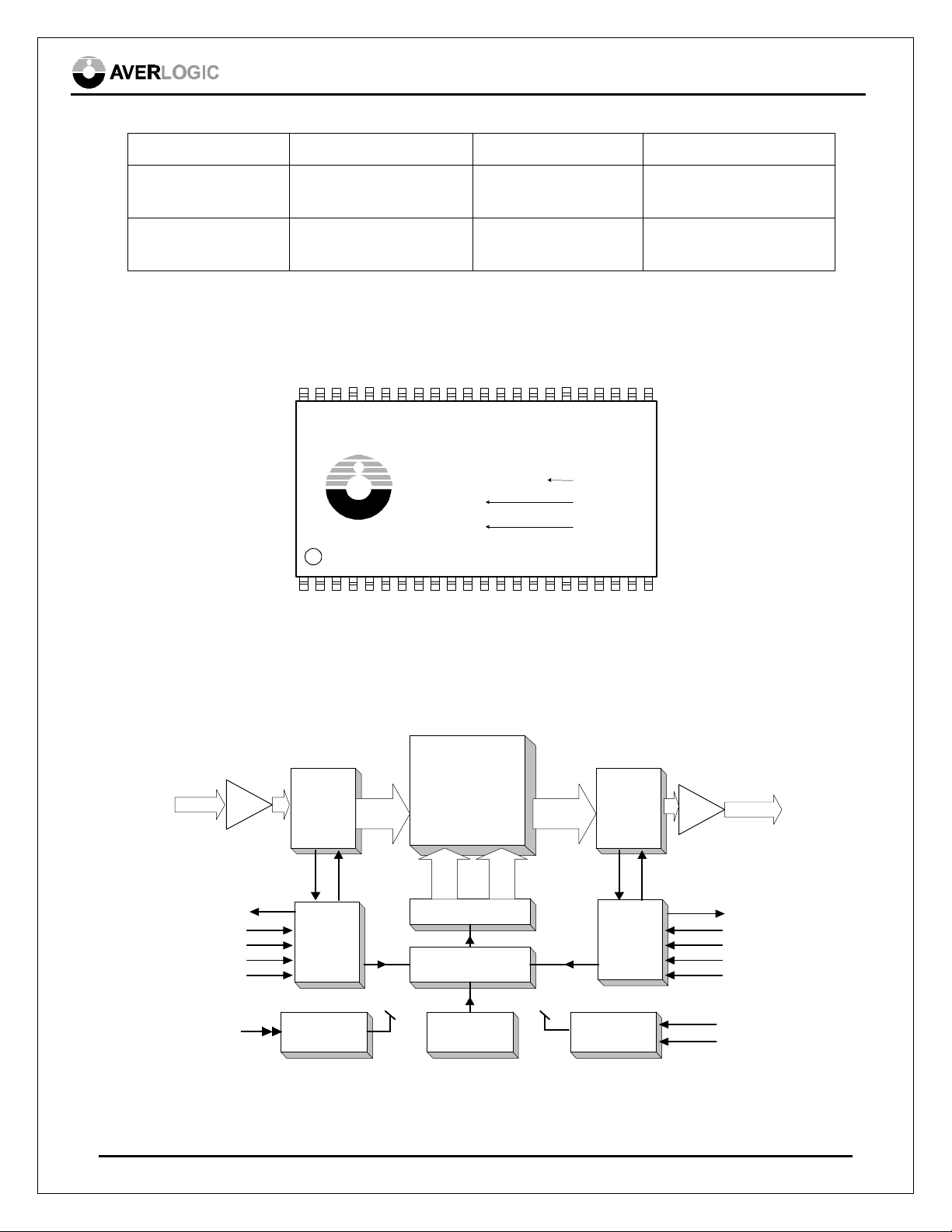
5.0 Pin-out Diagram
The AL440B pin-out diagram is following.
DO5
DO4
VDD
DO3
DO2
DO1
DO0
AVERLOGIC
1
2 3 4 5 6 7 8 9 10 11 12 13 14 15 16 17 18 19 202122
DI0
DI1
DI2
DI3
DI4
DI5
VDD
+3.3V±10%
+3.3V±10%
DO6
DO7
RE
OE
GND
RCK
RRST
AL440B-XX
XXXXX
XXXX
DI6
IE
DI7
WE
GND
WCK
WRST
ORDY
IRDY
VDD
/PLRTY
NC
TEST
/RESET
GND
Speed
Lot Number
Date Code
NCNCNC
AVDD
SDA
Sample Dec., 2001
Sample Dec.., 2001
SCL
23242526272829303132333435363738394041424344
AGND /SDAEN
6.0 Block Diagram
DI[7:0]
WRST
/SDAEN
SCL &
SDA
IRDY
WCK
WE
Input
Buffer
IE
Write
Data
Register
Iutput
Control
Control
Registers
AL440B-12/24 TSOP (II) pinout diagram (Top view)
512kx8 memory
Internal
Bus
cell array
Bus
Control
Memory Control
Timing Generator
& Arbiter
To all
Modules
Refresh
Counter
AL440B Block Diagram
Bus
Address
Internal
Bus
To all
Modules
Read
Data
Register
Output
Control
Timing &
Logic Control
Output
Buffer
DO[7:0]
ORDY
RCK
RRST
OE
RE
/PLRTY
/RESET
AL440B November 28, 2001 5
Page 6
AL440B
IRDY is a status output flag that reports the FIFO
RCK is the read clock input pin. The read data
The internal structure of the AL440B consists of an Input/Output buffers, Write Data Registers, Read
Data Registers and main 512k x8 memory cell array and the state-of-the-art logic design that takes
care of addressing and controlling the read/write data.
7.0 Pin Definition and Description
The pin definitions and descriptions are as follows:
Write Bus Signals
Pin name Pin number I/O
type
DI[7:0] 9,8,7,6,4,3,2,1 I The DI pins input 8bits of data. Data input is
synchronized with the WCK clock. Data is acquired
at the rising edge of WCK clock.
WE 10 I WE is an input signal that controls the 8bit input
data write and write pointer operation.
IE 11 I IE is an input signal that controls the enabling/
disabling of the 8bit data input pins. The internal
write address pointer is always incremented at rising
edge of WCK by enabling WE regardless of the IE
level.
WCK 13 I WCK is the write clock input pin. The write data
input is synchronized with this clock.
WRST 14 I The WRST is a reset input signal that resets the
write address pointer to 0.
IRDY 15 O
space availability.
Description
*Note: For the polarity definition of all write control signals (WE, IE, WRST and IRDY), please refer
to /PLRTY pin definition and “Memory Operation” section for details.
Read Bus Signals
Pin name Pin number I/O
type
DO[7:0] 36,37,38,39,
41,42,43,44
O The DO pins output 8bit of data. Data output is
synchronized with the RCK clock. Data is output at
the rising edge of the RCK clock.
RE 35 I RE is an input signal that controls the 8bit output
data read and read pointer operation.
OE 34 I OE is an input signal that controls the enabling/
disabling of the 8bit data output pins. The internal
read address pointer is always incremented at rising
edge of RCK by enabling RE regardless of the OE
level.
RCK 32 I
AL440B November 28, 2001 6
Description
Page 7
AL440B
ORDY is a status output flag that reports the FIFO
output is synchronized with this clock.
RRST 31 I The RRST is a reset input signal that resets the read
address pointer to 0.
ORDY 30 O
data availability.
*Note: For the polarity definition of all read control signals (RE, OE, RRST and ORDY), please refer
to /PLRTY pin definition and “Memory Operation” section for details.
Serial Port Bus Signals
Pin name Pin number I/O
type
SDA 25 I/O SDA carries the serial bus read/write data bits. The
SDA data bit is valid when the SCL is high after
start up sequence.
SCL 24 I SCL supplies the serial bus clock signal to FIFO.
The serial data bit is valid when the SCL is high
after start up sequence.
/SDAEN 23 I /SDAEN controls the enabling/disabling of serial
bus interface. When /SDAEN is high, the serial
interface is disabled and SDA pin is high
impedance. When /SDAEN is low, the serial
interface is enabled and data can be written to or
read from the FIFO registers.
Description
Power/Ground Signals
Pin name Pin number I/O
type
VDD 5, 29, 40 -
3.3V ± 10%.
GND 12, 26, 33 - Ground.
AVDD 18 - Dedicated power pin for the internal oscillator. 3.3V
± 10%.
AGND 22 - Dedicated ground pin for the internal oscillator.
Description
Miscellaneous Signals
Pin name Pin number I/O
type
/RESET 27 I The global reset pin /RESET will automatically
initialize chip logic. For the recommended circuit
for the global reset signal, please refer to the
Application Notes.
Description
AL440B November 28, 2001 7
Page 8
AL440B
/PLRTY 16 I Select active polarity of the control signals including
WE, RE, WRST, RRST, IE, OE, IRDY and ORDY
totally 8 signals
/PLRTY = VDD, active low.
/PLRTY = GND, active high.
Note: during memory operation, the pin must be
permanently connected to VDD or GND. If
/PLRTY level is changed during memory operation,
memory data is not guaranteed.
TEST 17 I For testing purpose only. No connect or connect to
Ground.
NC 19,20,21,28 - No connect or connect to Ground
8.0 Register Definition
There are some built-in registers in the AL440B that allows performing some optional functions such
as window read/write access. These registers can be programmed via serial bus (SDA, SCL and
/SDAEN). The serial bus interface protocol is illustrated in “Serial Bus Interface” chapter. The
serial bus control software code or tool is available at Averlogic Technologies, Inc. upon request.
8.1 Register Set
Address
00h COMPANYID R Company ID (46h)
02h WSTART_L R/W Window write starting address (Low byte)
03h WSTART_H R/W Window write starting address (High byte)
04h WXSIZE_L R/W Window write horizontal size (Low byte)
05h WXSIZE_H R/W Window write horizontal size (High byte)
06h WSTRIDE_L R/W Window write strike size (Low byte)
07h WSTRIDE_H R/W Window write strike size (High byte)
08h WYSIZE_L R/W Window write vertical size (Low byte)
09h WYSIZE_H R/W Window write vertical size (High byte)
0Ah WWCTRL R/W Window write control register
0Bh RSTART_L R/W Window read starting address (Low byte)
0Ch RSTART_H R/W Window read starting address (High byte)
0Dh RXSIZE_L R/W Window read horizontal size (Low byte)
0Eh RXSIZE_H R/W Window read horizontal size (High byte)
0Fh RSTRIDE_L R/W Window read strike size (Low byte)
10h RSTRIDE_H R/W Window read strike size (High byte)
11h RYSIZE_L R/W Window read vertical size (Low byte)
Register R/W
Description
2’s complement (for Y-mirror)
2’s complement (for Y-mirror)
[7]: enable window write function
[6]: X mirror
[5]: freeze
AL440B November 28, 2001 8
Page 9
AL440B
12h RYSIZE_H R/W Window read vertical size (High byte)
13h RWCTRL R/W Window read control register
[7]: enable window read function
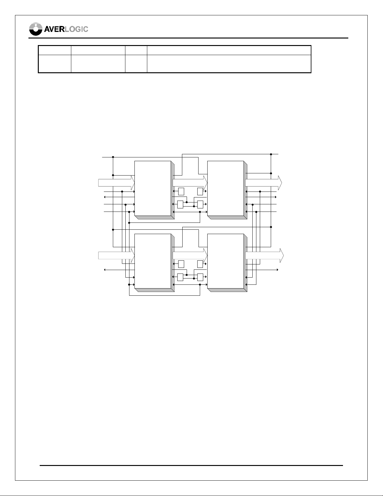
9.0 Multiple Devices Bus Expansion and Cascading
The AL440B FIFO memory can be applied to very wide range of media applications. A parallel
connect or cascade of multiple AL440B FIFOs provides FIFO bus width or memory depth expansion
for some applications; eg. accommodating HDTV resolution.. etc.
Write Reset
Read Reset
AL440
DI[7:0]
DO[7:0]
FIFO Empty
Write Enable
Write Clock
8-bit Input
FIFO Empty
(1) Logic Block: "OR" Gate if /PLTY = HIGH, "AND" Gate if /PLTY = HIGH
(2) Always Enabled : Tie to LOW if /PLTY = HIGH, Tie to High if /PLTY = LOW
IE OEInput Enable
IRDY
WE
WCK
AL440
WRST
DO[7:0]
IE IE
IRDY
WE
WCK
10.0 Serial Bus Interface
AL440
RRSTWRST
8-bit Output
ORDY
RCK
RRST
ORDY
RCK
(2)
(1) (1)
RE
8-bit OutputDI[7:0]
OE OE
(2) (2)
RE
AL440B Expanding & Cascading
WRST
DI[7:0]
IE
(2)
IRDY
WE
WCK
AL440
WRST
DI[7:0]
IRDY
(1)(1)
WE
WCK
RRST
DO[7:0]
OE
ORDY
RE
RCK
RRST
DO[7:0]
ORDY
RE
RCK
8-bit Output8-bit Input
Output Enable
FIFO Full
Read Enable
Read Clock
8-bit Output
FIFO Full
The serial bus interface consists of the SCL (serial clock), SDA (serial data) and /SDAEN (serial
interface enable) signals. There are pull up circuit internally for both SCL and SDA pins. When
/SDAEN is high, the serial bus interface is disabled and both SCL and SDA pins are pulled high.
When /SDAEN is low, the serial bus interface is enabled and data can be written into or read from the
AL440B register set. For both read and write, each byte is transferred MSB first and LSB last, and
the SDA data bit is valid when the SCL is pulled high. The serial bus control sample C code is
available in Averlogic Technologies, Inc. upon request.
The read/write command format is as follows:
Write: <S> <Write SA> <A> <Register Index> <A> <Data> <A> <P>
AL440B November 28, 2001 9
Page 10

AL440B
Read: <S> <Write SA> <A> <Register Index> <A> <S> <Read SA> <A> <Data> <NA> <P>
Following are the details:
<S>:
Start signal
SCL SDA
High High
High Low
The Start signal is HIGH to LOW transition on the SDA line when SCL is HIGH.
<WRITE SA>:
Write Slave Address: 0h
<READ SA>:
Read Slave Address: 1h
<REGISTER INDEX>:
Value of the AL440B register index.
<A>:
Acknowledge stage
The acknowledge-related clock pulse is generated by the host (master). The host releases the SDA
line (HIGH) for the AL440B (slave) to pull down the SDA line during the acknowledge clock
pulse.
<NA>:
Not Acknowledged stage
The acknowledge-related clock pulse is generated by the host (master). The host releases the SDA
line (HIGH) during the acknowledge clock pulse, but the AL440B does not pull it down during
this stage.
<DATA>:
Data byte write to or read from the register index.
In read operation, the host must release the SDA line (high) before the first clock pulse is
transmitted to the AL440B.
<P>:
Stop signal
SCL SDA
High Low
High High
The Stop signal is LOW to HIGH transition on the SDA line when SCL is HIGH.
Suppose data F0h is to be written to register 0Fh using write slave address 0h, the timing is as
follows:
AL440B November 28, 2001 10
Page 11

SDA
SCL
AL440B
Start Slave addr = 0h Ack Ack Ack StopIndex = 0Fh Data = F0h
AL440B Serial bus Write timing
Suppose data is to be read from register 05h using read slave address 1h, the timing is as follows:
Start
Slave addr = 0h
SDA
SCL
Ack
Stop
Ack AckIndex = 05h
AL440B Serial bus read timing
Start
Read slave addr = 1h
NAck
11.0 Memory Operation
11.1 Power-On-Reset & Initialization
During the system power on, a 200µs negative pulse on the /RESET pin is required and will
automatically initialize chip logic. Apply a valid reset pulse to WRST and RRST after power-onreset to reset read/write address pointer to zero.
StopData read cycle
11.2 WRST, RRST Reset Operation
The reset signal can be given at any time regardless of the WE, RE and OE status, however, they still
need to meet the setup time and hold time requirements with reference to the clock input. When the
reset signal is provided during disabled cycles, the reset operation is not executed until cycles are
enabled again.
11.3 Control Signals Polarity Select
The AL440B provides the option for operating polarity on controlling signals. With this feature the
application design can benefit by matching up the operation polarity between AL440B and an
existing interfacing devices without additional glue logic. The operating polarity of control signals
WE, RE, WRST, RRST, IE, OE, IRDY and ORDY are controlled by /PLRTY signal. When
/PLRTY is pulled high all 8 signals will be active low. When /PLRTY is pulled low all 8 signals will
be active high.
AL440B November 28, 2001 11
Page 12

AL440B
11.4 FIFO Write Operation
In the FIFO write operation, 8 bits of write data are input in synchronization with the WCK clock.
The FIFO write operation is determined by WRST, WE, IE and WCK signals and the combination of
these signals could produce different write result. The /PLRTY signal determines the activated
polarity of these control signals. The following tables describe the WRITE functions under different
operating polarities.
/PLRTY = VDD
WRST WE IE WCK Function
L - -
Write reset.
↑
The write pointer is reset to zero.
H L L
H L H
Normal Write operation.
↑
Write address pointer increases, but no new data will be
↑
written to memory. Old data is retained in memory.
(Write mask function)
H H -
Write operation stopped. Write address pointer is also stopped.
↑
/PLRTY = GND
WRST WE IE WCK Function
H - -
L H H
L H L
L L -
Write reset.
↑
The write pointer is reset to zero.
Normal Write operation.
↑
Write address pointer increases, but no new data will be
↑
written to memory. Old data is retained in memory.
(Write mask function)
Write operation stopped. Write address pointer is also stopped.
↑
11.5 FIFO Read Operation
In the FIFO read operation, 8 bits of read data are available in synchronization with the RCK clock.
The access time is stipulated from the rising edge of the RCK clock. The FIFO read operation is
determined by RRST, RE, OE and RCK signals, so the combination of these signals could produce
varying read results. The /PLRTY signal could decide the activated polarity of these control signals.
The following tables describe the READ functions under different operating polarities.
/PLRTY = VDD
RRST RE OE RCK Function
L L L
L L H
L H L
AL440B November 28, 2001 12
Read reset. The read pointer is reset to zero.
↑
Data in the address 0 is output.
Read reset. The read pointer is reset to zero.
↑
Output is high impedance.
Read address pointer is stopped. Output data is held. Read
↑
address pointer will be reset to zero and data in the address 0 is
output after RE goes low.
Page 13

AL440B
L H H
Read address pointer is stopped. Output data is held. Read
↑
address pointer will be reset to zero and output is high
impedance after RE goes low.
H L L
H L H
Normal Read operation.
↑
Read address pointer increases. Output is high impedance.
↑
(Data skipping function)
H H L
H H H
Read address pointer is stopped. Output data is held.
↑
Read operation stopped. Read address pointer is stopped.
↑
Output is high impedance.
/PLRTY = GND
RRST RE OE RCK Function
H H H
H H L
H L H
H L L
L H H
L H L
L L H
L L L
When the new data is read, the read address should be between 192 and 524,287 cycles after the write
address pointer, otherwise the output for new data is not guarantee.
Read reset. The read pointer is reset to zero.
↑
Data in the address 0 is output.
Read reset. The read pointer is reset to zero.
↑
Output is high impedance.
Read address pointer is stopped. Output data is held. Read
↑
address pointer will be reset to zero and data in the address 0 is
output after RE goes low.
Read address pointer is stopped. Output data is held. Read
↑
address pointer will be reset to zero and output is high
impedance after RE goes low.
Normal Read operation.
↑
Read address pointer increases. Output is high impedance.
↑
(Data skipping function)
Read address pointer is stopped. Output data is held.
↑
Read operation stopped. Read address pointer is stopped.
↑
Output is high impedance.
11.6 IRDY, ORDY Flags
The IRDY, ORDY flags indicate the status of FIFO. The IRDY signal reports whether or not there is
space available for writing new data to the FIFO. An ORDY signal reports whether or not there is
valid new data available at output. The IRDY and ORDY signals only report the status of the address
pointer; they will not stop or affect the read/write operations. The following tables describe the
IRDY/ORDY functions under different operating polarities.
/PLRTY = VDD
Signal State Function
H No more free space is available for new input data IRDY
L Memory space is available for new input data.
ORDY H No new data is available in FIFO memory.
AL440B November 28, 2001 13
Page 14

AL440B
L New data are available in the FIFO memory.
/PLRTY = GND
Signal State Function
H Memory space is available for new input data. IRDY
L No more free space is available for new input data
H New data are available in the FIFO memory. ORDY
L No new data is available in FIFO memory.
11.7 Window Write Register Programming
Window data read/write is supported in the AL440B to benefit the designing effort for applications
such as PIP display. The window mode is enabled by driving low on /SDAEN signal. A serial bus
can program built-in registers to set up coordinates of the window and the settings take effect
following by next read/write reset pulse. Window mirroring can cooperate with the window mode
data access to flip window data in x or y direction. When window-mirroring function is turned on,
write data can be stored in reverse sequence.
The serial communication interface consists of 3 signals, they are SCL (serial clock), SDA (serial
data) and /SDAEN (window mode enable). The serial communication interface is enabled by driving
low on /SDAEN signal. The detail operation timing of the serial bus is illustrated in chapter 10. In
Window read/write mode, read and/or write may begin at the start address of any of the 8192 blocks.
Each block is 64 bytes in length. (8192 blocks x 64 byte = 512 kbytes)
0
1
Block number:
Memory size: 8192 blocks x 64 bytes = 512 kbytes
2
64 bytes each block
AL440B Window mode block address
The Window Write related registers are listed as follows:
WSTART_L and WSTART_H define the widow data write starting address.
Addr Name Bit7 Bit6 Bit5 Bit4 Bit3 Bit2 Bit1 Bit0
02h WSTART_L [7] [6] [5] [4] [3] [2] [1] [0]
03h WSTART_H 0 0 0 [12] [11] [10] [9] [8]
WSTART (Write Start address) <= WSTART_H[4:0] & WSTART_L ;
WSTART range is from 0 to 8191 (block).
8189
8190
8191
AL440B November 28, 2001 14
Page 15

AL440B
WXSIZE_L and WXSIZE_H define the window data write horizontal size.
Addr Name Bit7 Bit6 Bit5 Bit4 Bit3 Bit2 Bit1 Bit0
04h WXSIZE_L [7] [6] [5] [4] [3] [2] [1] [0]
05h WXSIZE_H 0 0 0 0 0 0 [9] [8]
WXSIZE (Write X Size) <= WXSIZE_H[2:0] & WXSIZE_L ;
WXSIZE range is from 0 to 1023 (block).
WXSTRIDE_L and WXSTRIDE_H define the window data write horizontal width.
Addr Name Bit7 Bit6 Bit5 Bit4 Bit3 Bit2 Bit1 Bit0
06h WSTRIDE_L [7] [6] [5] [4] [3] [2] [1] [0]
07h WSTRIDE_H 0 0 0 [12] [11] [10] [9] [8]
WSTRIDE (Write Stride) <= WSTRIDE_H[4:0] & WSTRIDE _L ;
WSTRIDE range is from –4096 to +4095 (block).
When the value of WSTRIDE is negative, it is used to implement Y-Mirror function.
WYSIZE_L and WYSIZE_H define the window data write vertical high.
Addr Name Bit7 Bit6 Bit5 Bit4 Bit3 Bit2 Bit1 Bit0
08h WYSIZE_L [7] [6] [5] [4] [3] [2] [1] [0]
09h WYSIZE_H [15] [14] [13] [12] [11] [10] [9] [8]
WYSIZE (Write Y Size) <= WYSIZE_H & WYSIZE_L ;
Write Y Size range is from 0 to 65535 (unsign).
WWCTRL is the register that control window data write function enable/disable and the window
mirroring write.
Addr Name Bit7 Bit6 Bit5 Bit4 Bit3 Bit2 Bit1 Bit0
0Ah WWCTRL [7] [6] [5] 0 0 0 0 0
WWCTRL[7] Window Write mode enable
1: enable Window Write mode
0: disable Window Write mode. The memory is operating in standard FIFO write
mode.
WWCTRL[6] X-mirror function enable
1: enable X-mirror function
0: disable X-mirror function
WWCTRL[5] Freeze function enable. This function is as same as hardware “Write Mask” function.
When Window Write mode is enabled, software freeze function override hardware
Write Mask function. On the other hand, in FIFO mode (WWCTRL[7] = ‘0’), Register
WWCTRL[5] is ignored.
1: enable software Freeze function
0: disable software Freeze function
A mirroring read/write function can be cooperated with the window-block data access function. By
turning on the mirroring read/write function in the window block access mode, write data can be
AL440B November 28, 2001 15
Page 16

AL440B
stored in reversed sequence. For some applications like video conferencing, this function can correct
reciprocal positioning of a captured object.
Please refer the following diagrams which illustrate Window Write operation.
Memory Area
WSTART
WSTART+1xWSTRIDE
WSTART+2xWSTRIDE
WYSIZE
WSTART+(WYSIZE-1)x WSTRIDE
Memory Area
WSTART-XSIZE+1
Write Window Area
WXSIZE
WXSIZE
Go back to WSTART
WSTART
WSTART+(XSIZE-1)
Normal Write Window:
WWCTRL[6]: 0
No X-mirror
WSTRIDE: postive numer
No Y-mirror
AL440B Write Window(1)
WSTART+1xWSTRIDE
X-mirror Write Window:
WSTART+2xWSTRIDE
WWCTRL[6]: 1
X-mirror
WYSIZE
WSTRIDE: postive numer
No Y-mirror
Go back to WSTART
Write Window Area
WSTART+(WYSIZE-1)x WSTRIDE
AL440B-03 Write Window(2)
AL440B November 28, 2001 16
Page 17

Memory Area
AL440B
WSTART+(WYSIZE-1)x WSTRIDE
WSTART-XSIZE+1
Write Window Area
Go back to WSTART
WXSIZE
WYSIZE
WSTART+2xWSTRIDE
WSTART+1xWSTRIDE
WSTART
X-mirror & Y-mirror
Write Window:
WWCTRL[6]: 1
X-mirror
WSTRIDE: negative numer
Y-mirror
AL440B Write Window(3)
11.8 Window Read Register Programming
The operations of Window Read function are same as Window Write. The operation of Window
Read is operated independently from Window Write. The Window Read related registers are listed as
follows:
RSTART_L and RSTART_H define the widow data read starting address.
Addr Name Bit7 Bit6 Bit5 Bit4 Bit3 Bit2 Bit1 Bit0
0Bh RSTART_L [7] [6] [5] [4] [3] [2] [1] [0]
0Ch RSTART_H 0 0 0 [12] [11] [10] [9] [8]
RSTART (Read Start address) <= RSTART_H[4:0] & RSTART_L ;
RSTART range is from 0 to 8191 (block).
RXSIZE_L and RXSIZE_H define the window data read horizontal size.
Addr Name Bit7 Bit6 Bit5 Bit4 Bit3 Bit2 Bit1 Bit0
0Dh RXSIZE_L [7] [6] [5] [4] [3] [2] [1] [0]
0Eh RXSIZE_H 0 0 0 0 0 0 [9] [8]
RXSIZE (Read X Size) <= RXSIZE_H[2:0] & RXSIZE_L ;
WXSIZE range is from 0 to 1023 (block).
RXSTRIDE_L and RXSTRIDE_H define the window data write horizontal width.
Addr Name Bit7 Bit6 Bit5 Bit4 Bit3 Bit2 Bit1 Bit0
0Fh RSTRIDE_L [7] [6] [5] [4] [3] [2] [1] [0]
10h RSTRIDE_H 0 0 0 0 [11] [10] [9] [8]
RSTRIDE (Read Stride) <= RSTRIDE_H[3:0] & RSTRIDE _L ;
RSTRIDE range is from 0 to +4095 (block).
AL440B November 28, 2001 17
Page 18

AL440B
RYSIZE_L and RYSIZE_H define the window data read vertical high.
Addr Name Bit7 Bit6 Bit5 Bit4 Bit3 Bit2 Bit1 Bit0
11h RYSIZE_L [7] [6] [5] [4] [3] [2] [1] [0]
12h RYSIZE_H [15] [14] [13] [12] [11] [10] [9] [8]
RYSIZE (Read Y Size) <= RYSIZE_H & RYSIZE_L ;
Write Y Size range is from 0 to 65535.
RWCTRL is the register that control window data read function enable/disable .
Addr Name Bit7 Bit6 Bit5 Bit4 Bit3 Bit2 Bit1 Bit0
13h RWCTRL [7] 0 0 0 0 0 0 0
RWCTRL[7] Read Write mode enable
1: enable Window Read mode
0: disable Window Read mode. The memory is operating in standard FIFO Read
mode.
Note:
1. X-mirror and Y-mirror functions are not needed in Window Read mode, so they are not
implemented in Window Read operation.
2. There is no “freeze” function in Window Read mode.
Please refer to the following illustration as an application example for the explanation of Window
read operation.
RSTART+1xRSTRIDE
RSTART+2xRSTRIDE
RSTART+ (RYSIZE-1)x RSTRIDE
Memory Area
RSTART
RYSIZE
RXSIZE
Go back to RSTART
Read Window Area
AL440B Read Window
RSTART+ (RXSIZE-1)
AL440B November 28, 2001 18
Page 19

AL440B
12.0 Electrical Characteristics
12.1 Absolute Maximum Ratings
Parameter
VDD Supply Voltage -0.3 ~ +3.8 V
VP Pin Voltage -0.3 ~ +(VDD+0.3) V
IO Output Current -20 ~ +20 mA
T
Ambient Op. Temperature 0 ~ +85 °C
AMB
T
Storage temperature -40 ~ +125 °C
stg
12.2 Recommended Operating Conditions
Parameter Min Typ Max Unit
VDD Supply Voltage +3.0 +3.3 +3.6 V
VIH High Level Input Voltage 0.7 VDD VDD V
VIL Low Level Input Voltage 0 0.3 V
Rating
Unit
DD
V
12.3 DC Characteristics
(VDD = 3.3V, Vss=0V. T
Parameter Min Typ Max Unit
IDD Operating Current - 52 62 mA
I
Standby Current - 14 - mA
DDS
VOH Hi-level Output Voltage 2.4 - VDD V
VOL Lo-level Output Voltage - - +0.4 V
ILI Input Leakage Current (No pull-up or pull-down) -5 - +5
ILO Output Leakage Current (No pull-up or pull-down)
RL Input Pull-up/Pull-down Resistance 50
1. Tested with outputs disabled (I
2. RCLK and WCLK toggle at 20 Mhz and data inputs switch at 10 Mhz.
AL440B November 28, 2001 19
= 0 to 70°C)
AMB
= 0)
OUT
µA
-5 - +5
µA
KΩ
Page 20

AL440B
12.4 AC Characteristics
(VDD = 3.3V, Vss=0V, T
Parameter
TWC WCK Cycle Time 25 - 12.5 - ns
T
WCK High Pulse Width 10 - 5 - ns
WPH
T
WCK Low Pulse Width 10 - 5 - ns
WPL
TRC RCK Cycle Time 25 - 12.5 - ns
T
RCK High Pulse Width 10 - 5 - ns
RPH
T
RCK Low Pulse Width 10 - 5 - ns
RPL
TAC Access Time - 20 - 12 ns
TOH Output Hold Time 6 - 4 - ns
THZ Output High-Z Setup Time 5 4 ns
TLZ Output Low-Z Setup Time 6 5 ns
T
WRST Setup Time 8 - 4 - ns
WRS
AMB
= 0 to 70°C)
40MHz 80MHz
Unit
Min Max Min Max
T
WRST Hold Time 8 - 5 - ns
WRH
T
RRST Setup Time 8 - 4 - ns
RRS
T
RRST Hold Time 8 - 5 - ns
RRH
TDS Input Data Setup Time 5 - 4 - ns
TDH Input Data Hold Time 6 - 5 - ns
T
WE Setup Time 6 - 4 - ns
WES
T
WE Hold Time 6 - 5 - ns
WEH
T
WE Pulse Width 15 - 12 - ns
WPW
T
RE Setup Time 6 - 4 - ns
RES
T
RE Hold Time 6 - 5 - ns
REH
T
RE Pulse Width 15 - 12 - ns
RPW
T
IE Setup Time 6 - 4 - ns
IES
T
IE Hold Time 6 - 5 - ns
IEH
T
IE Pulse Width 15 - 12 - ns
IPW
T
OE Setup Time 8 - 5 - ns
OES
T
OE Hold Time 8 - 5 - ns
OEH
T
OE Pulse Width 20 - 12 - ns
OPW
TTR Transition Time 3 3 ns
CI Input Capacitance - 7 - 7 pF
AL440B November 28, 2001 20
Page 21

AL440B
CO Output Capacitance - 7 - 7 pF
• The read address needs to be at least 192 cycles after the write address.
AL440B November 28, 2001 21
Page 22

AL440B
Reset
13.0 Timing Diagrams
cycle n
cycle (s)
WCK
T
TR
T
WRS
WRST
DI7~0
n-1 n 0 1
/PLRTY=VDD , WE= "L" , IE= "L"
Write Cycle Timing (Write Reset)
cycle n cycle n+1 Disable cycle (s)
cycle 0 cycle 1
T
WRH
TDST
DH
cycle n+2
T
WPL
WCK
T
WPH
T
T
WC
WES
T
WEH
WE
T
WPW
T
DSTDH
DI7~0
n-1 n
n+1 n+2
/PLRTY=VDD ,IE="L" ,WRST="H"
Write Cycle Timing (Write Enable)
AL440B November 28, 2001 22
Page 23

AL440B
cycle n cycle n+1 Disable cycle (s)
WCK
T
WPH
T
WRST
WE
DI7~0
n-1 n
/PLRTY=VDD ,IE="L"
cycle 0
T
WPL
WC
T
WES
TDST
DH
n+1 1
T
WRS
T
WEH
T
WPW
T
WRH
cycle 1
0
Write Cycle Timing (WE, WRST)
cycle n cycle n+1 cycle n+3
T
WPL
WCK
T
WPH
T
WC
IE
DI7~0
n-1 n
/PLRTY=VDD ,WE="L" ,WRST="H"
cycle n+2 cycle n+4
T
IES
T
IPW
T
IH
n+1
T
IEH
n+4
Write Cycle Timing (Input Enable)
AL440B November 28, 2001 23
Page 24

AL440B
Reset
cycle n
cycle (s)
TRPL
cycle 0 cycle 1
RCK
TRPH
TRRS TRRH
RRST
TAC
TOH
DO7~0
n-1 n
0 1
0
/PLRTY=VDD ,RE= "L" ,OE= "L"
Read Cycle Timing (Read Reset)
cycle n cycle n+1 Disable cycle (s)
T
RPL
RCK
T
RPH
T
RC
RE
T
AC
T
OH
DO7~0
n-1 n
/PLRTY=VDD ,OE="L" ,RRST="H"
Read Cycle Timing (Read Enable)
cycle n+2
T
RES
T
RPW
n+1
T
REH
n+2
AL440B November 28, 2001 24
Page 25

AL440B
cycle n cycle n+1 Disable cycle (s)
RCK
T
RPH
T
RRST
RE
DO7~0
n-1 n
/PLRTY=VDD,OE="L"
cycle 0
T
RPL
RC
T
RRS
T
RES
T
AC
T
OH
T
RRH
T
REH
T
RPW
n+1
0
Read Cycle Timing (RE, RRST)
cycle n cycle n+1 cycle n+3
T
RPL
RCK
T
RPH
T
RC
OE
T
DO7~0
n-1 n
/PLRTY=VDD ,RE="L" ,RRST="H"
cycle n+2
T
OES
T
OPW
T
AC
T
OH
HZ
n+1
T
OEH
Hi-Z
cycle n+4
T
LZ
n+4
Read Cycle Timing (Output Enable)
AL440B November 28, 2001 25
Page 26

AL440B
Reset
cycle n
cycle (s)
WCK
T
TR
T
WRS
WRST
DI7~0
n-1 n 0 1
/PLRTY=GND , WE= "H" , IE= "H"
Write Cycle Timing (Write Reset)
cycle n cycle n+1 Disable cycle (s)
cycle 0 cycle 1
T
WRH
TDST
DH
cycle n+2
T
WPL
WCK
T
WPH
T
WC
WE
T
DSTDH
DI7~0
n-1 n
/PLRTY=GND ,IE="H" ,WRST="L"
Write Cycle Timing (Write Enable)
T
WES
T
WPW
n+1 n+2
T
WEH
AL440B November 28, 2001 26
Page 27

AL440B
cycle n cycle n+1 Disable cycle (s)
WCK
T
WPH
T
WC
WRST
WE
DI7~0
n-1 n
/PLRTY=GND ,IE="H"
T
WPL
TDST
T
WRS
T
WES
T
WPW
DH
n+1 1
T
WEH
Write Cycle Timing (WE, WRST)
T
WRH
cycle 0
cycle 1
0
cycle n cycle n+1 cycle n+3
T
WPL
WCK
T
WPH
T
WC
IE
DI7~0
n-1 n
/PLRTY=GND ,WE="H" ,WRST="L"
Write Cycle Timing (Input Enable)
cycle n+2 cycle n+4
T
IES
T
IPW
T
IH
n+1
T
IEH
n+4
AL440B November 28, 2001 27
Page 28

AL440B
Reset
cycle n
cycle (s)
TRPL
cycle 0 cycle 1
RCK
TRPH
TRRS TRRH
RRST
TAC
TOH
DO7~0
n-1 n
0 1
0
/PLRTY=GND ,RE= "H" ,OE= "H"
Read Cycle Timing (Read Reset)
cycle n cycle n+1 Disable cycle (s)
T
RPL
RCK
T
RPH
T
RC
RE
T
AC
T
OH
DO7~0
n-1 n
/PLRTY=GND ,OE="H" ,RRST="L"
Read Cycle Timing (Read Enable)
cycle n+2
T
RES
T
RPW
n+1
T
REH
n+2
AL440B November 28, 2001 28
Page 29

AL440B
cycle n cycle n+1 Disable cycle (s)
RCK
T
RPH
T
RC
RRST
RE
DO7~0
n-1 n
/PLRTY=GND ,OE="H"
cycle 0
T
RPL
T
RRS
T
RES
T
AC
T
OH
T
RRH
T
REH
T
RPW
n+1
0
Read Cycle Timing (RE, RRST)
cycle n cycle n+1 cycle n+3
T
RPL
RCK
T
RPH
T
RC
OE
T
T
OH
DO7~0
n-1 n
/PLRTY=GND ,RE="H" ,RRST="L"
cycle n+2
T
OES
T
OPW
AC
T
HZ
n+1
T
OEH
Hi-Z
cycle n+4
T
LZ
n+4
Read Cycle Timing (Output Enable)
AL440B November 28, 2001 29
Page 30

AL440B
14.0 Mechanical Drawing – 44 PIN PLASTIC TSOP (II)
AL440B November 28, 2001 30
Page 31

“D
(Unit: mm)
“b”
NOTE:
1. Controlling Dimension : Millimeters.
2. Dimension “D” does not include mold protrusion. Mold protrusion shall not exceed 0.15(0.006”)
per side. Dimension “E1” does not include interlead protrusion. Interlead protrusion shall not
exceed 0.25(0.01”) per side.
3. Dimension “b” does not include damar protrusions/intrusion. Allowable damar protrusion shall
not cause the lead to be wider than the MAX “b” dimension by more than 0.13mm. Damar
intrusion shall not cause the lead to be narrower than the MIN “b” dimension by more than
0.07mm.
AL440B November 28, 2001 31
Page 32

15.0 Application Notes
15.1 Chip Global Reset Recommend Circuit
To ensure a proper reset pulse can be applied to /RESET pin (pin 27) to complete the power-on reset,
the recommend reset circuit is to connect the AL440B /RESET pin (pin 27) to VDD with a 2k Ω
resistor and to Ground with a 10µf capacitor as follows.
AL440B
8-bit Input 8-bit Output
DI[7:0]
DO[7:0]
/RESET
50K
Ohm
2K
Ohm
27
10 uf
AL440B Global Reset Circuit
VDD
It is also recommend adding buffers for the power-on reset circuit to increase the driving capability
for any application with multiple AL440B chips.
15.2 The AL440B Reference Schematic
U8
2K
C54
10uF
RNSMD1 10
2
3
4
R5 10
0.1uf
+
C55
R3 2K
FDVDD
0.1uf
WE
IE
WCK
WRST
IRDY
VDD3S
Populate R2 or R3 to select
Control Singals polarity
VDD3S
R2
1 2
F B
L5 FB
C56
81
7
6
5
0.1uf
C57
DI0
DI1
DI2
DI3
DI4
DI5
DI6
DI7
CTL0
CTL1
CTL2
CTL3
CTL4
CTL5
AL440
1
DI0
2
DI1
3
DI2
4
DI3
6
DI4
7
DI5
8
DI6
9
DI7
10
WE
11
IE
14
WRST
15
IRDY
16
PLRTY
17
TEST
5
VDD
29
VDD
VDD
12
GND
26
GND
33
GND
NC
28
NC
NC
1939204021
DO0
DO1
DO2
DO3
DO4
DO5
DO6
DO7
RCKWCK
RRST
ORDY
SDA
SCL
SDAEN
/RESET
AVDD
AGND
NC
RE
OE
DO0
44
DO1
43
DO2
42
DO3
41
DO4
DO5
38
DO6
37
DO7
36
RNSMD3 10
CTL7
35
CTL8
34
3213
31
30
25
24
23
27
18
22
2
CTL9
3
CTL10
4
CTL11
CTL12
2
CTL13
3
CTL14
4
RNSMD4 10
R5 10
FAVDD VDD3S
1 2
0.1uf
C62
F B
L7 FB
R6
R7
81
7
6
5
81
7
6
5
4.7K
4.7K
R1 2K
RE
OE
RCK
RRST
ORDY
SDAEN
VDD3S
VDD3S
+
C67
10uF
SDA
SCL
AL440B November 28, 2001 32
Page 33

CONTACT INFORMATION
AverLogic Technologies, Inc.
90 Great Oaks Blvd. #204
San Jose, CA 95119
USA
Tel : +1 408 361-0400
Fax : +1 408 361-0404
E-mail : sales@averlogic.com
URL : www.averlogic.com
AverLogic Technologies, Corp.
4F., No.514, Sec.2, Cheng Kung Rd.,
Nei-Hu Dist., Taipei, Taiwan
R.O.C
Tel : +886 2-27915050
Fax : +886 2-27912132
E-mail : sales@averlogic.com.tw
URL : www.averlogic.com.tw
 Loading...