

Page 1
Alesis Semiconductor
DS3201-08 02 12555 Jefferson Blvd., Sui te 285
Los Angeles, CA 90066
Phone (310) 301-0780 Fax (310) 306-1551 www.alesis-semi.com
We make the parts that set creative people free
General Description
The AL3201 (SCR, or Single Chip Reverb)
is a one chip reverb solution that is
compact, easy to use, and yet quite
powerful. Built-in DRAM eliminates the
need for wide bus c onnections to external
RAM, and the choice of built-in programs
and a user programmable RAM allows
instant usability or custom program
design.
Features
16 internal ROM programs consisting
of halls, rooms, plates, delays, chorus,
flange, vocal cancel, and rotary
speaker emulation.
Serially programmable SRAM (Writable
Control Store – WCS) for program
development or dynamically changing
programs
Programs run at 128 instructions per
word clock. (6 MIPS @ 48kHz sampling frequency.)
32k location DRAM provides over 0.6 8s
of delay at 48kHz sampling frequency.
Internal crystal oscillator circuit
eliminates need for discrete external
passive components.
Internal voltage regulators allow opera-
tion at both 5V an d 3.3V V
DD
.
Internal 1000pF bypass capacitor to
reduce voltage swings at the rails.
Applications
Personal stereos with reverb functions.
Extremely portable guitar effects boxes.
Karaoke machines utilizing the vocal cancel program.
Hardware reverb ef fects for computer so und cards.
Ambience settings for car stereos.
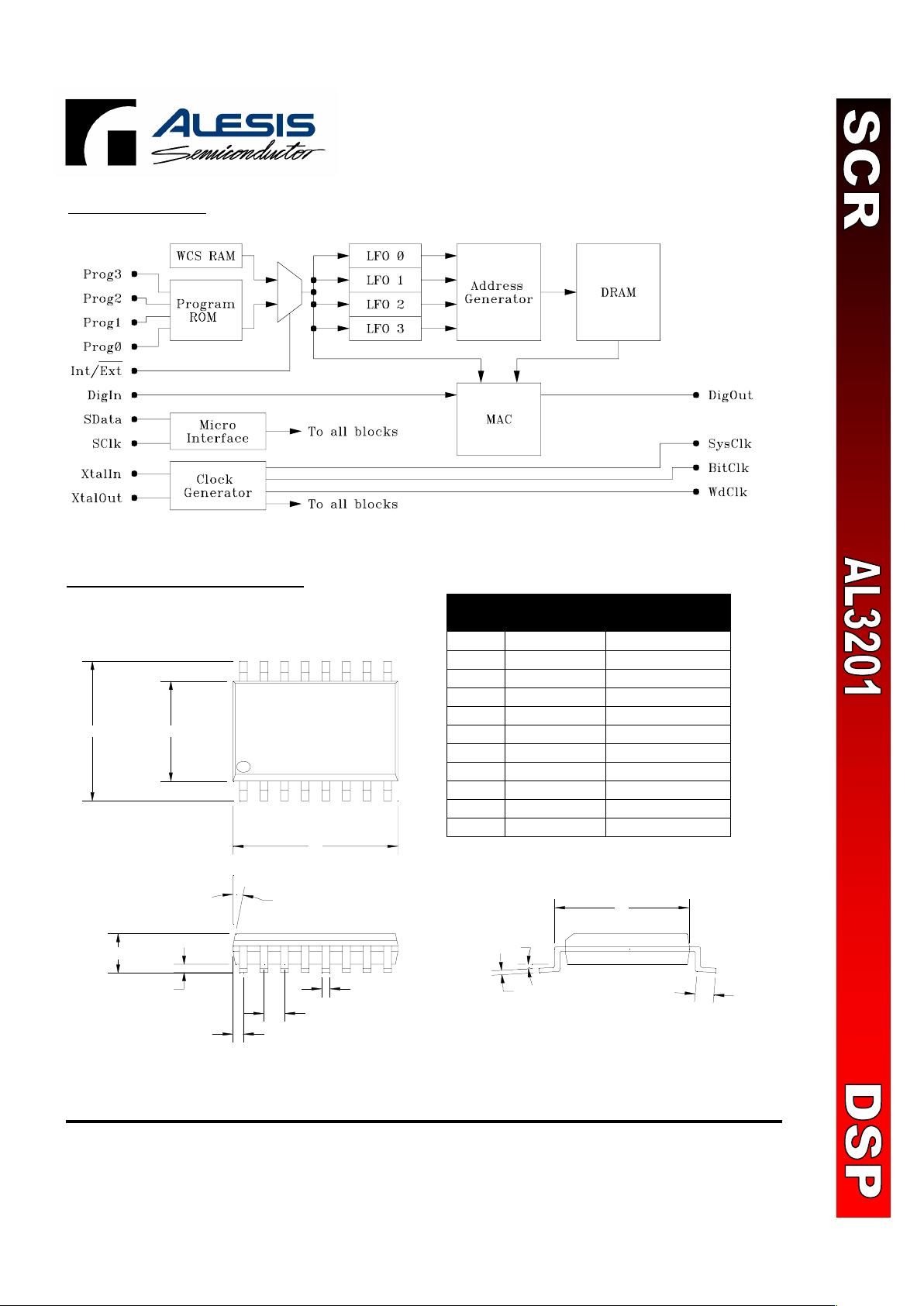
DigOut
Int/Ext
XtalIn
XtalOut
Prog0/SData
Prog1/SClk
Prog2
Prog3
DigIn
Bypass
Gnd
Reset
SysClk
BitClk
WordClk
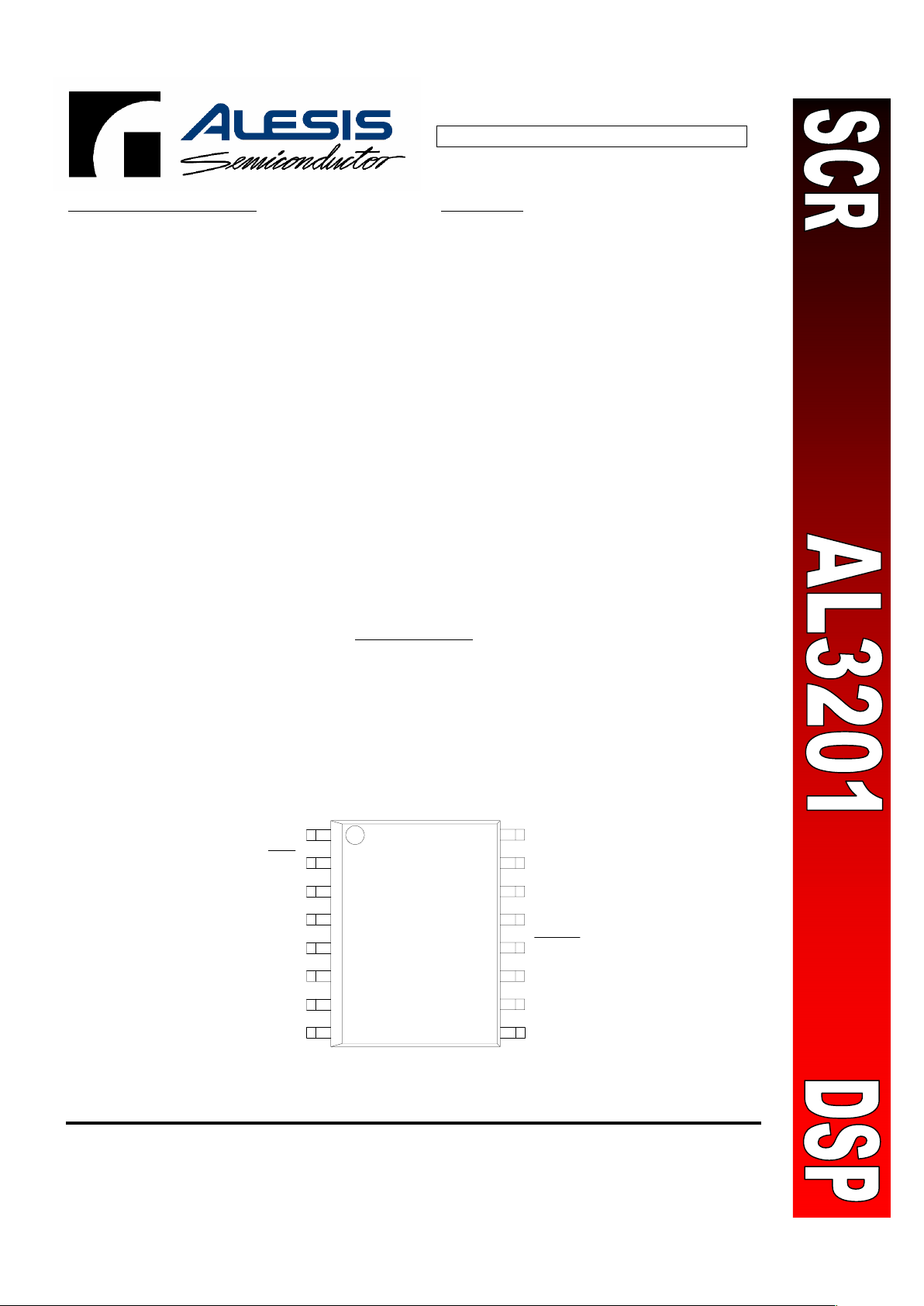
16 pin SOIC
300 mils wide
1
8
1
6
9
V
DD
A
L
3
2
0
1
S
C
R
Page 2
Alesis Semiconductor
DS3201-08 02 12555 Jefferson Blvd., Sui te 285
Los Angeles, CA 90066
Phone (310) 301-0780 Fax (310) 306-1551 www.alesis-semi.com
-
2 -
Electrical Characteristics and Operating Conditions
Parameter Description Condition Min Typ Max Units
Electrical Characteristics and Operating Conditions
VDD Supply Voltage 3.0/4.5 3.3/5.0 3.6/5.5 V
IDD Supply Current : SCR 6/9 7/10 8/11 mA
Gnd Ground Note 3 - 0.0 - V
FS Sample rate 24
1
48 50
1
kHz
Temp
Temperature
0 25 70
°C
Outputs (DigOut, SysClk, BitClk, WordClk)
VOH Logical “1” output voltage Unloaded 0.9 VDD VDD - V
VOL Logical “0” output voltage Unloaded - 0 0.05 VDD V
IOH Logical “1” output current VDD=5V VO=4.5V - - -8.0 mA
IOL Logical “0” output current VDD=5V VO=0.4V - - 8.0 mA
_______________ __________________________
Inputs (DigIn, Int/Ext, Prog0/Sdata, Prog1/SClk, Prog2, Prog3, Reset) Notes 2,4
VIH Logical “1” input voltage 2.5 - VDD V
VIL Logical “0” input voltage 0 - 0.5 V
IIH Logical “1” input current
V
DD=VIH
=5V
- - 2
µA
IIL Logical “0” input current
No pullup pin
- - 2
µA
I
ILP
Logical “0” input current
Pullup pin, Vin=0
83 167 333
µA
CIN Input Capacitance - 2.0 - pF
Note:
1. Changing the sample rate (by changing the crystal frequency) will change the maximum delay
available through the DRAM proportionally. Low sample rates require mor e refresh instructio ns.
2. XtalIn, XtalOut are special pins designed to be connected to a crystal. XtalOut is a relatively weak pin
(about 0.2 mA) and should not be used to drive external circuits. Instead of using a crystal, XtalIn
may be driven by a standard V
DD
to Gnd logic signal, but the logic levels are n ot specified.
3. All other voltages are relative to Gnd.
4. Bypass (pin 14) must never exceed 3.6V
Pin Descriptions: AL3201 SCR (*: Pullup to V
DD
via nominal internal 30kΩ resistor)
Pin # Name Pin Type Description
1 DigOut Output Digital serial output for stereo DAC.
2
______________
Int/Ext
Input* Internal/extern al program sel ection. 1:Internal, 0: External.
3 XtalIn Input 12.288MHz crystal input.
4 XtalOut Output 12.288MHz crystal output.
5 Prog0/SData Bidirectional* Internal program select 0 / serial i n terface data lin e.
6 Prog1/SClk Input* Internal program select 1 / serial interface clock line.
7 Prog2 Input* Internal progr a m select 2.
8 Prog3 Input* Internal progr a m select 3.
9 WordClk Output Word clock output.
10 BitClk Output Bit clock output.
11 SysClk Output System clock output.
12
________________ _____
Reset
Input Active low reset.
13 Gnd Ground Ground connection.
14 Bypass Bidirectional
Connect 0.1µF bypass capacitor to Gnd for internal +3.3V regulator.
15 V
DD
Power
+5V/+3.3V V
DD
power pin. Connect 0.1µF capacitor to Gn d.
16 DigIn Input Digital serial input fr om stereo ADC.
Page 3
Alesis Semiconductor
DS3201-08 02 12555 Jefferson Blvd., Sui te 285
Los Angeles, CA 90066
Phone (310) 301-0780 Fax (310) 306-1551 www.alesis-semi.com
-
3 -
Block Diagram
Mechanical Specification
1
8
916
E
D
F
H
G
L
K
7° nom
BC
4° nom
J
A
Dimensions (T ypical)
Inches Millimeters
A
.406”
10.31
B .295” 7.49
C .407” 10.34
D .100” 2.50
E .008” 0.20
F .025” 0.64
G .050” 1.27
H .017” 0.42
J .011” 0.27
K .340” 8.66
L .033” 0.83
Notes:
1) Dimension “A” do es not include mo ld
flash, protrusions or gate burrs.
Page 4

Alesis Semiconductor
DS3201-08 02 12555 Jefferson Blvd., Sui te 285
Los Angeles, CA 90066
Phone (310) 301-0780 Fax (310) 306-1551 www.alesis-semi.com
-
4 -
Internal Programs
The SCR comes with 16 internal ROM
programs ready to go, utilizing the skills
and techniques of the Alesis Studio
Electronics effects proce ssor pr ogramm ers.
By setting the chip to internal mode, the
four program pins may be used to select
between the different algorithms.
Program List
Prg Name Description
0* Delay 1
125ms slapbac k d el ay f or
vocals and guitars.
1 Chorus/Room 2
Auto-wah guitar effect with
reverb for lead instruments.
2 Hall 2
Warm hall for acoustic
guitars, pianos, and vocals.
3 Vocal Cancel
Removes lead vocals from
many s tereo recordings.
4* Delay 2
190ms delay for p ercussive
arpeggios.
5 Chorus/Room 1
Chorus with reverb for
guitars, synths, and pianos.
6 Hall 1
Bright hall reverb for
drums, guitars, and v ocals.
7 Rotary Speaker
Rotary speaker emulation
for organs and guitars.
8 Flange
Stereo flanger for jet wash
effects.
9 Plate 2
Sizzling bright plate reverb
for vocals and drum s.
10 Room 1
Hardwood studio for
acoustic instruments.
11 Plate 1
Classic plate reverb for lead
vocals and instruments.
12* Chorus
Stereo chorus for guit ar s
and pianos.
13 Plate 3
Short vintage plate reverb
for snares and guitars.
14 Room 2
Ambience for acoust i c
mixes and synth sounds.
15 Room 3
Warm room for guitars and
rhythm instruments.
Note: The unusual ordering of the programs allows a
16-position rotary switch’s Gray code output to be
connected to the program pins. The sequence of
programs is then Halls 1-2, Rooms 1-3, Plates 1-3,
Chorus, Flange, Delays 1-2, Chorus/Rooms 1-2,
Vocal Canc el, and Rota ry Speaker.
*
WARNING
Programs 0, 4, and 12 do not meet refresh
requirements. Do not depend upon these programs
working in any application.
Page 5

Alesis Semiconductor
DS3201-08 02 12555 Jefferson Blvd., Sui te 285
Los Angeles, CA 90066
Phone (310) 301-0780 Fax (310) 306-1551 www.alesis-semi.com
-
5 -
Programming the RAM
Alongside the 16 internal programs is an
externally programmable SRAM that is
easily accessible through the serial clock
and data pins. By setting the chip to
external mode, the SClk and SData pins
become available for serial
communication. Except for its external
programmability, there is no functional
difference between the SRAM and the
internal ROMs.
Memory Map
Addr Name
Addr Name
0:3 LFO Coefficients
0:127 WCS RAM
4:127 MAC Instructions
128 Control/Status 0
129 Control/Status 1
A simple assembly language is available
for writing programs. With th e assembler
and loader software available from the
Alesis Semiconductor website, programs
may be developed on the PC and
downloaded into the chi p. Please refer to
the assembly language guide for a full
description.
LFO Coefficient Word
Bit # Description
31 P: Pitch shift mode s elect (S must be set).
1
30 S: Sine/triangle select. 1:Triangle; 0: Sine.
X[1:0] Xfade
11 1/16
10 1/8
01 1/2
29:28
X[1:0]: Crossfa de
coefficient select. Value
indicates the fraction of a
half sawtooth period
used in crossfading.
00 1
27:15 F[12:0]: Frequency coefficient, unsigned.
14:0 A[14:0]: Amplitude coefficient, un signed.
Note:
If set, the outpu t waveform is a sawtoo th with do uble
the triangle wave’s frequency.
Sawtooth SIN
Sawtooth COS
Crossfade 1
Crossfade 1/2
Crossfade 1/8
The first four instructions in the WCS RAM
set the parameters for the four LFOs. The
sinusoid generated by the LFOs is of the
formula Asin(nF/M) or Acos(nF/M), where
n is the time index, F/M = 2πf/F
S
, M is the
maximum internal value, f is the select ed
frequency, and F
S
is the sampling
frequency. Thus the frequency extrema
are:
f
= (F/M) FS/(2π)
f
min
= (0x1/0x3ffff) (48kHz)/(2π)
= 0.029Hz
f
max
= (0x1fff/0x3ffff) (48kHz)/(2π)
= 239Hz
Triangle waves are gener ated by incre mentally adding or subtractin g 0x400000*F/M
(= 2
22
*F/M) from the maximum internal
negative or positive value res pectively. Its
frequency extrema are then:
f
= # Samples / # Steps
= F
S
/ (4 Max/Increment)
= F
S
/ (4 0x7fffff/(222*F/M))
f
min
= 48kHz / (8/(0x1/0x3ffff))
= 0.023Hz
f
max
= 48kHz / (8/(0x1fff/0x3ffff))
= 187Hz
When chorus instructions are used,
addresses are offset by t he output an LFO.
The range of this offset is plus and min us
A/8 samples, or A/4 sa mples total.
Following the 4 LFO coefficient words are
124 MAC instruction words. These
instructions allow the manipulation of the
DRAM and the waveforms generated by
the LFOs.
A good NOP instruction is 0x00030000.
This instruction preserves th e value in all
registers, and is the NOP executed in the
MAC during the first four ticks of every
sample period while the LFO coefficients
are loaded.
By judiciously choosing the LFO fr equency
and waveform with which to sweep
through the DRAM, it is possible to
generate pitch shifts, flanges, choruses,
reverbs, and other effects. Please see
application notes for descriptions and
examples.
Page 6

Alesis Semiconductor
DS3201-08 02 12555 Jefferson Blvd., Sui te 285
Los Angeles, CA 90066
Phone (310) 301-0780 Fax (310) 306-1551 www.alesis-semi.com
-
6 -
MAC Instruction Word
Bit # Description
31 S: Sign bit for multiplier coefficient.
C[7:1]: Multiplier coefficient, 2’s compl ement.
C[7:0]: Chorus instruction. Only the 7 MSBs
are used as multiplier coefficients. The LSB is
used in chorus mode. If I[5] is set, C[7:0] is:
C Description
7
Chorus/Xfade select:
1: Pass LFO address to address
generator & select chorus coefficient.
0: Mask LFO addres s t o ad dress
generator & select cros sf ade coefficient.
6
1’s complement t h e LF O address sign
bit.
1
5 1’s complement the LFO coefficient.
4 1’s complement the LF O address.
3
LFO latch. 1: Latch in new LFO data;
0: Hold last LFO data.
2
2:1 LFO select.
30:23
0 LFO sine/cosine select. 1: Cos; 0: Sin .
22 W: Write select.
3, 4
I[5:0]: Instructi on f ield.
I Description
5
Chorus select (When set, MAC
coefficient is LFO block output, LFO
address offset added to DRAM
address).
4 Clock register C.
3
3 Clock register B.
4
2 Reserved – set to zero.
I[1:0] Instruction
11 Acc = Prod + Acc
6
10 Acc = Prod + C
3
01 Acc = Prod + B
5
21:16
1:0
MAC
product
instruction.
00 Acc = Prod + 0
15:0
A[15:0]: Multiplicand address.
7, 8
(Currently
only lower 15 bits used; reserve MSB for
future expansion.)
Address 0x00 00 = LeftIn/Out;
Address 0x00 01 = R ig h tIn/Out.
Notes:
1.
This complement is only for the MSB, and sign-
extension bits are not af f ect ed.
2.
Upon latching new data, the LFO registers will
store the lower or upper LFO pairs’
sinusoid/triangle waves , and the lower or upper
LFO pairs’ crossfade coefficient. I.e. there are
two pairs of registers; LFO 0/1’s sinusoid
/triangle/crossfade will be latched together, and
LFO 2/3’s sinusoid/triangle/crossfade will be
latched together.
3.
The LeftOut, RightOut, and C registers are in
parallel with the accumulator, and will contain
the same value as the accumulator if clocked at
the end of the tick.
4.
A write to DRAM stores the last tick’s results into
address A. Writes to Le ftOu t or RightOu t sho uld
use the Acc = Product + Acc instruction with the
multiplier coefficient set to 0 to pass all bits
unaltered.
5.
Register B, if clocked at the end of the tick, will
store the value of the current tick’s multiplicand.
When a read is executed, B latches LeftIn,
RightIn, or DRAM. When a write is executed, B
latches the accumulator from the last tick.
6.
The accumulator contains the result from the
last instruction tick, and is updated at the end of
the current instruction ti ck.
7.
The internal DRAM address offset automatically
decrement s by 1 every w ord cl ock period.
8.
Because addresses 0x0000 and 0x0001 are
being used to access the left and right channels ,
those DRAM memory locations may not be
directly written to or read from.
Page 7

Alesis Semiconductor
DS3201-08 02 12555 Jefferson Blvd., Sui te 285
Los Angeles, CA 90066
Phone (310) 301-0780 Fax (310) 306-1551 www.alesis-semi.com
-
7 -
Control/Status Word 0
Bit # Description
31:30 Res erved. Set to zero.
29:16 B[13:0] : DRAM read data.
1
15:11 Res erved. Set to zero.
10
O: MAC overflow. Self-clears after read. Read
only.
9 P: Self test pass. Read only.
8
R: Ready indication. Read/write/test/clear
complete.
7
M: DigOut mute in external mode. Resets
to 1.
6
Z: DRAM zero. Initiates zeroing cycles until
deasserted. Resets to 0.
2, 3, 4, 5, 6
5
X: DRAM zero cancel. Prevents zeroing
circuitry from running until deasserted.
Overrides Z. Resets to 0.
3
4
L: LFO reset pulse. Resets LFO internal
status registers and clears overflow flag. Self
clearing. Resets to 0.
3
I: Instruction RAM dir ect mode. Resets to 1.
1: Instructions are written/read as soon as
received; 0: Instructi on s are written/read
when the address c ounter rolls around to
matching address.
7
2 Reserved. Set to zero.
1
S[1]: DRAM self test pattern select.
1: Load DRAM with 2AAA/1555 checkerboard;
0: Load DRAM with 1555/2AAA checkerboard.
0
S[0]: DRAM self test initiate. Self-clears after
test completion. Resets to 0.
2, 3, 6, 8, 9
Notes:
1.
The floating point format used in the DRAM is:
E[2:0].S.F[9:0], where E is the exponent, S is the
sign bit, and F is the fractional portion. The
expansion of the floati ng point into fixe d point is
as follows:
If E<7, S E*S !S FFFFFFFFFF (8-E)* 0
(where E*S means E number of S bits).
If E=7, S SSSSSSS FFFFFFFFFF 00.
This method encodes one ex tra bit for sign
extensions less than 7 bit s.
2.
The DRAM zeroing circuitry and DRAM self te st
circuitry share gates; do not turn more than one
on at a time.
3.
The DRAM zeroing cycle will run to completion
even if Z deasserted. Only the X bit may cancel
it mid-cycle. Until the cycle ends, self test
results will be inaccurate. Thus do not deassert
Z and assert S[0] at the same time. Rather,
assert X and S[0] at the sam e t ime.
Note that Z does not self-clear, and will affect
both internal and external mode.
4.
After a DRAM zeroing cycle has completed, do
not start another for one word clock period.
5.
A DRAM zeroing cycle takes approximately
5.33ms to complete with a 12MHz crystal.
6.
During DRAM zeroing and test cycles, reads and
writ es to th e DRAM a re ignored.
7.
For dynamically changing programs, deassert I
so that changing the program does not interrupt
its execution. Otherwise reads and writes to the
Instruction RAM will usurp the address bus to
the RAM and cause address jumps in the
instruction sequence. With I deasserted, reads
and writes to each address may take up to one
word clock period to complete. Thus during
continuous writes, the start of each instruction
word should be at least one word clock period
apart, and during reads the serial clock should
wait 1 word clock after the address before
continuing.
8.
The DRAM self test cycle will run to completion
even if S[0] is deasserted. It may not be
cancelled.
9.
A DRAM self test cycle takes approximately
10.66ms to com plete with a 12MHz crys t al .
Control/Status Word 1
Bit # Description
31
R: Read select. Read data from DRAM
address A[15:0] an d put data in B of
control/status word 0. S elf-clears after
completion.
30
W: Write select. Wr i t e data D[13:0] to DRAM
address A[15:0]. Self-clear s af t er c ompletion.
29:16 D[13: 0]: DRAM write da t a.
15:0
A[15:0]: DRAM address. The MSB is unused
and reserved for future expansion.
Note: Reading and writing DRAM will usurp DRAM
access for one cycle, possibly disrupting proper code
execution.
Other notes:
1. When in internal mode, program
changes will start a DRAM zero cycle.
2. Resets alw ays start a DRAM zero cycle.
3. To meet refresh requir ements below 70
°C, access each address (modulo 1024)
every 1.34 ms. I f program code does n't
do this, then (at 48 kHz) read 16
locations each cycle spa ced 1024/16 =
64 addresses apart, to meet refresh
requirements. (For insta nce, addresses
0x0002, 0x0042, ..., 0x03C2.)
4. ROMs may not be read due to the
serial interface becoming the program
select interface when in internal mode.
5. Use of Reset is mandatory to obtain
proper operation of t h e AL32 01.
The 4 word formats: L F O , MAC, CS0, CS1
LFO: PSXXFFFF FFFFFFFF FAAAAAAA AAAAAAAA
MAC: SCCCCCCC CWIIIIII AAAAAAAA AAAAAAAA
CS0: --BBBBBB BBBBBBBB -----OPR MZXLI-SS
CS1: RWDDDDDD DDDDDDDD AAAAAAAA AAAAAAAA
Page 8

Alesis Semiconductor
DS3201-08 02 12555 Jefferson Blvd., Sui te 285
Los Angeles, CA 90066
Phone (310) 301-0780 Fax (310) 306-1551 www.alesis-semi.com
-
8 -
Serial Interface Format
The basic format for the micro serial inter f ace is:
Attn Sel R/W A7 A6 A5 A4 A3 A2 A1 A0 DN DN-1 D N-2 … D2 D1 D0 Attn Desel
⇓ ⇓
Attn: A 0-1-0 is used to signal attention/start. Write mode only
Sel/Desel: 0:Select; 1:Deselect. A7 - A0: Address
R/W: 0:Read; 1:Write DN - D0: Data
Notes:
1.
The re is a short period of High-Z du ring a read
between A0 and the first data bit shifted out.
This period must be at least 5 system clocks
long, 1 word clock long if not in direct mode
(CS0[3]).
2.
A s long as data is being sent during a write, the
address will be automatically incremented.
Therefore only a start address need be sent.
3.
The phase o f the clock i s unimportant.
Page 9

Alesis Semiconductor
DS3201-08 02 12555 Jefferson Blvd., Sui te 285
Los Angeles, CA 90066
Phone (310) 301-0780 Fax (310) 306-1551 www.alesis-semi.com
-
9 -
DigIn/DigOut Interface Format
Suggested Connections
Page 10

Alesis Semiconductor
DS3201-08 02 12555 Jefferson Blvd., Sui te 285
Los Angeles, CA 90066
Phone (310) 301-0780 Fax (310) 306-1551 www.alesis-semi.com
-
10 -
NOTICE
Alesis Semiconductor reserv es the right to make changes to their products or to disc ontinue
any product or service w ithout notic e. All product s are sold subject to terms and c onditions
of sale supplied at the time of order acknowledgement. Alesis Semiconductor assumes no
responsibility for the use of any circuits described herein, conveys no license under any
patent or other right, and makes no representation that the circuits are free of patent
infringement. Information contained herein are only for illustration pur poses and may vary
depending upon a user’s specific application. While the information in this publication has
been carefully checked, no responsibility is assumed for inaccuracies.
Alesis Semiconductor products are not designed for use in applications which involve
potential risks of d eath, personal injury, or severe property or env ironmental damage or life
support applications where the failure or malfunction of the product can reasonably be
expected to cause failure of the life support system or to significantly affect its safety or
effectiveness.
All trademarks and registered trademarks are property of their r espect ive owners.
Contact Information:
Alesis Semiconductor
12555 Jefferson Blvd., Suite 285
Los Angeles, CA 90066
Phone: (310) 301-0780
Fax: (310) 306-1551
Email: sales@alesis-semi.com
Copyright 20 02 Alesis Semiconductor
Datasheet August 2002
Reproduction, in part or in whole, without the prior written consent of Alesis
Semiconductor is prohibited.
 Loading...