

Page 1

AL250/251 Data Sheets
Page 2

AL250
Contents
1.0 Features ___________________________________________________________________ 3
2.0 Applications ________________________________________________________________ 3
3.0 General Description__________________________________________________________ 4
4.0 Pinout Diagrams ____________________________________________________________ 5
5.0 Pin Definition and Description _________________________________________________ 6
6.0 Functional Description _______________________________________________________ 8
6.1 Digital Input/Output Data Formats __________________________________________________8
6.2 Default Resolution________________________________________________________________9
6.3 Video Timing ____________________________________________________________________9
6.4 Border/Border Color ____________________________________________________________13
6.5 OSD Interface __________________________________________________________________14
6.6 External Overlay________________________________________________________________15
6.7 Look-up Table (LUT) ____________________________________________________________16
6.8 I2C Programming _______________________________________________________________16
6.9 Video Decoding _________________________________________________________________18
7.0 Electrical Characteristics ____________________________________________________ 20
7.1 Recommended Operating Conditions _______________________________________________20
7.2 Characteristics__________________________________________________________________20
8.0 AL250/251 Register Definition________________________________________________ 22
8.1 Register Description _____________________________________________________________23
9.0 Board Design and Layout Considerations _______________________________________ 29
9.1 Grounding _____________________________________________________________________29
9.2 Power Planes and Power Supply Decoupling _________________________________________29
9.3 Digital Signal and Clock Interconnect _______________________________________________29
9.4 Analog Signal Interconnect________________________________________________________29
10.0 Mechanical Drawing_______________________________________________________ 30
11.0 Power Consumption _______________________________________________________ 32
July 28, 1999 2
Page 3
AL250/251 Video Scan Doubler
1.0 Features
• Convert interlaced TV signal (NTSC/PAL) into
non-interlaced RGB format for CRT monitors
or LCD panels
• Highly integrated design with built-in DAC,
SRAM, OSD and LUT
• Built-in on-screen-display with programmable
bitmap
• Interpolated scan doubling with no tearing or
jagged edge artifacts
• Reduced interlace flicker
• Auto NTSC/PAL detect
• Digital video input of square pixel, ITU-RBT
601 (CCIR 601), or user-defined format
• Analog/digital non-interlaced RGB (VGA)
signal output (Scan Doubled or Deinterlaced)
• I2C programming interface
• Power-down control via I2C
AL250
• Internal RGB video lookup table (LUT) to
provide gamma correction and special effects
• Overlay support for title making and complex
on-screen display
• Self-initialization without software (Plug &
Play)
• 3.3 or 5 volt support
• 16-bit digital RGB/YUV output (AL251 only)
2.0 Applications
• TV-ready Multimedia Computer Monitor
• TV to PC Video Scan Converter Box
• Progressive Scan TV
• Video Game Station
• DVD Player
• LCD TV Monitor
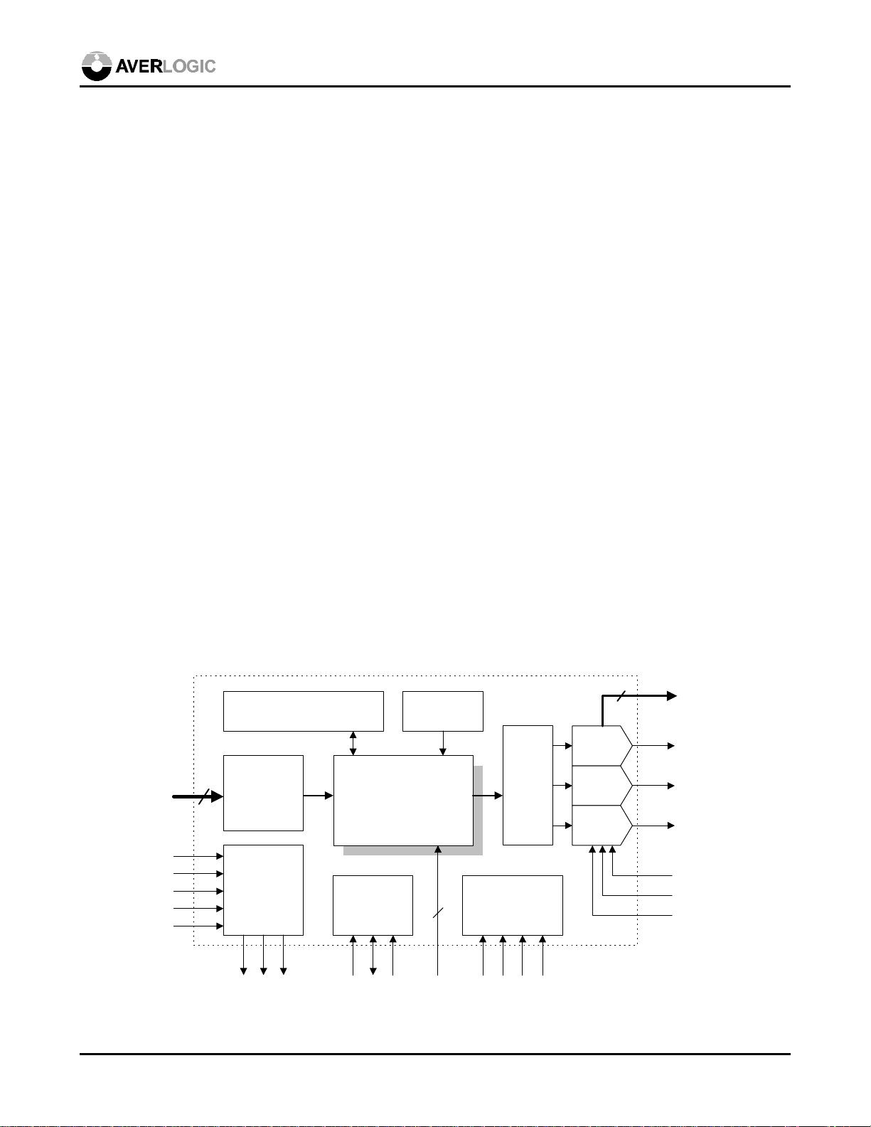
Digital
YUV or RGB
input
VCLK
VCLKX2
VIDHS
VIDVS
HREF
16
Video Memory
Video
Formatter
Timing
Control
GVS
GHS
GHREF
On-screen
Display
Video Processor
and Scan Doubler
I2C Circuit
2
SCL
SDA
CADDR
2
I
OVLCTRL
RGB
Video
Lookup
Tables
Mode Control
STD
RESET
INTYPE
8-bit DAC
8-bit DAC
8-bit DAC
SQUARE
16
AL250-01
Digital YUV or
RGB output
(AL251)
R
G
B
RSET
VREF
COMP
July 28, 1999 3
Page 4

AL250
3.0 General Description
The AL250/251 Video Scan Doubler (De-Interlacer) is a video conversion chip for consumer video
and multimedia applications. It converts interlaced NTSC or PAL, ITU-RBT 601 (CCIR 601) or
square pixel, YUV422 or RGB565 digital signals into computer monitor RGB signals for direct
connection to a computer monitor or progressive scan TV.
By using I2C interface control, the AL250/251 can also be programmed to co-ordinate with various
input resolutions, adjust screen positioning and crop video noise from around the original input video
boundary.
The internal RGB video lookup tables (LUT), which are controlled via I2C interface, can provide
gamma correction for calibrating the color accuracy of different types of CRT’s and improving the
contrast level to display more vivid pictures.
A built-in on-screen-display (OSD) provides programmable bitmap RAM for custom design icons and
on-screen control panels.
Overlay function is supported to create titling or on-screen-display menus for video adjustment.
The AL251 provides all the features of the AL250. Additionally, it has digital output in YUV422 or
RGB565 format, and can convert NTSC video for VGA LCD panels.
The AverLogic proprietary digital signal processing technology creates a highly stable video image
without tearing effects or jagged edges. The output picture is smoother and has less flicker than the
original input signal/picture.
July 28, 1999 4
Page 5
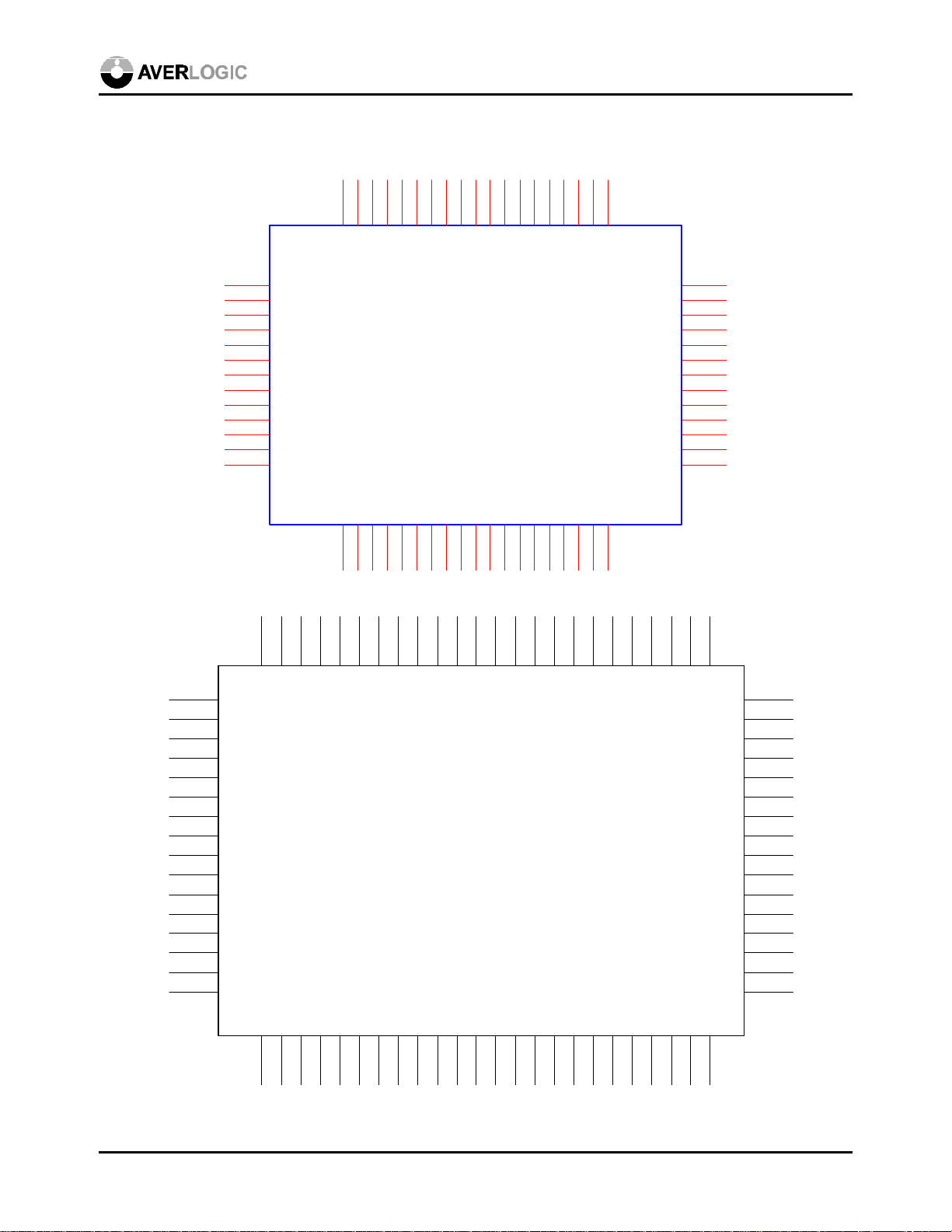
4.0 Pinout Diagrams
10
11
12
13
14
15
16
17
18
19
52
VDIN5
53
VDIN6
54
VDIN7
55
VDIN8
56
VDD
57
VDIN9
58
VDIN10
59
VDIN11
60
GND
61
VDIN12
62
VDIN13
63
VDIN14
64
VDIN15
51
50
VDIN4
VIDHS
49
48
VDIN3
VDIN2
VDD
VCLK
47
46
45
44
42
VDD43VDD
GND
VDIN1
VDIN0
TESTY7
TESTY6
AL250
VIDVS
VCLKX2
HREF
GND
STD0
STD1
41
40
TESTY5
INTYPE
GND
39
38
37
TESTY4
TESTY3
TESTY2
TESTIN
I2CADDR
SQUARE
36
35
34
TESTY1
TESTY0
OVLCTRL1
VDD
/RESET
SDA
33
GND
VREF
OVLCTRL0
COMP
RSET
AVDD
AGND
AG
AVDD
AB
AGND
GHS
GVS
GREF
SCL
VDD
AR
AL250
32
31
30
29
28
27
26
25
24
23
22
21
20
1
2
3
4
5
6
7
8
9
64636261605958
65
66
67
68
69
70
71
72
73
74
75
76
77
78
79
80
DO14
DO15
VDIN5
VDIN6
VDIN7
VDIN8
VDD
VDIN9
VDIN10
VDIN11
GND
VDIN12
VDIN13
VDIN14
VDIN15
NC
DO13
DO12
VDIN4
VDIN3
VDIN2
VDIN1
565554535251504948474645444342
57
DO5
DO4
DO3
DO2
GND
VDIN0
DO7
DO6
VDD
VDD
DO1
DO0
OVLCTRL1
AL251
GND
OVLCTRL0
41
NCNCNC
NC
VREF
COMP
RSET
AVDD
AR
AGND
AG
AVDD
AB
AGND
GHS
GVS
GREF
D011
D010
40
39
38
37
36
35
34
33
32
31
30
29
28
27
26
25
NC1NC2VIDHS3VDD4VCLK5VIDVS6GND7VCLKX2
NC
8
HREF9STD010STD111GND12INTYPE13SQUARE14TESTIN15I2CADDR16/RESET17SDA18VDD19SCL20VDD21DO822DO9
23
24
AL251-01 pinout diagram
July 28, 1999 5
Page 6
5.0 Pin Definition and Description
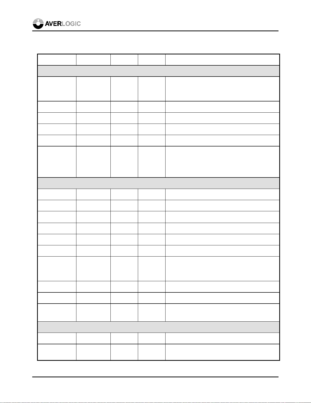
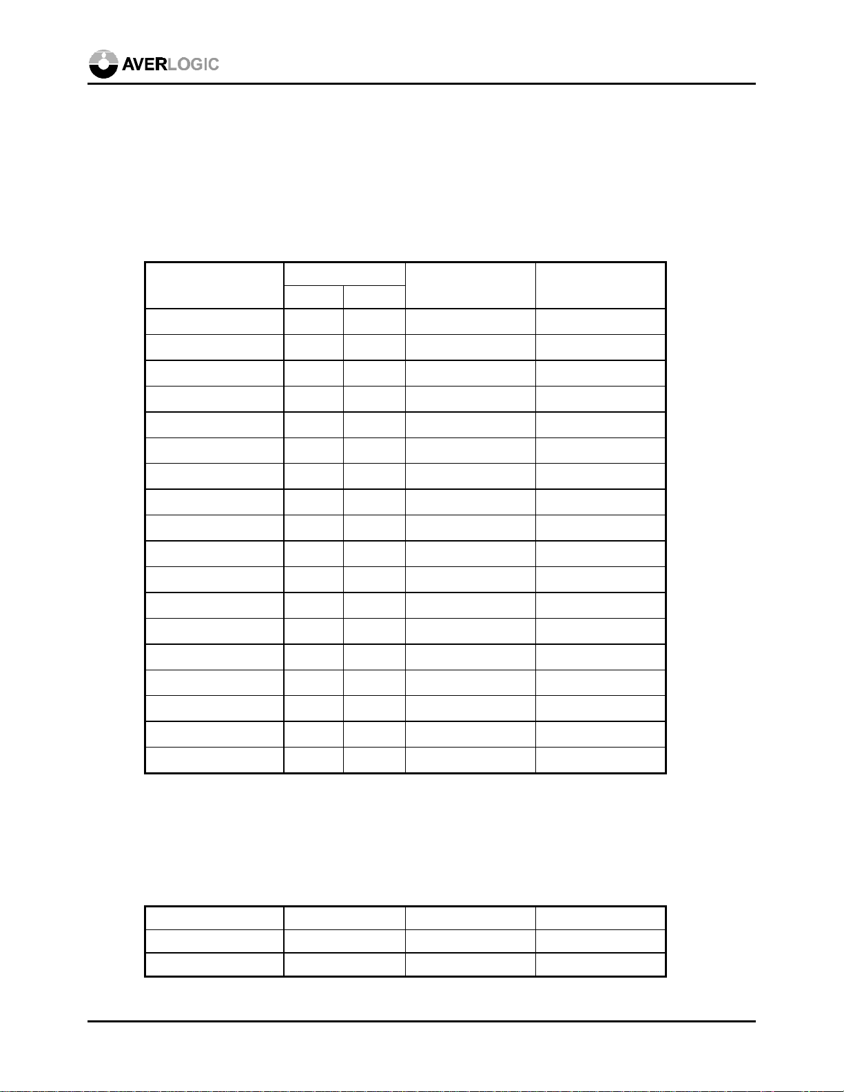
Symbol Type 250 Pin # 251 Pin # Description
Video Interface
AL250
VDIN (15 to 0) in (CMOS) 64-61, 59-
57, 55-52,
51-47
VCLK in (CMOS) 3 6 Video clock input
VCLKX2 in (CMOS) 6 9 2 times of video clock input
VIDHS in (CMOS) 1 4 Horizontal sync. input signal
VIDVS in (CMOS) 4 7 Vertical sync. input signal
HREF in (CMOS) 7 10 Horizontal reference input signal; this signal is
Graphic Interface
RSET In (100 ohm) 30 37 Full Scale Current Adjust; 100 ohm pull-down
VREF in (1.235V) 32 39 Voltage Reference Input
COMP
AR out (0.7V) 28 35 VGA analog red output
out (0.1µF)
31 38
79-76, 7472, 70-67,
62-58
Digital video data input. Please refer to the input
data format table for details
used to indicate data on the digital YUV bus. The
positive slope marks the beginning of a new
active line.
Compensation pin; 0.1µF pull-up
AG out (0.7V) 26 33 VGA analog green output
AB out (0.7V) 24 31 VGA analog blue output
DO (15 to 0) out (CMOS) N/A 66-63, 26-
23, 56-55,
52-47
GHS out (TTL) 22 29 VGA horizontal sync. output signal
GVS out (TTL) 21 28 VGA vertical sync. output signal
GHREF out (CMOS) 20 27 VGA horizontal reference output signal; it can be
Reset & Mode Select
/RESET in (CMOSd) 15 18 Reset input; active low
STD (1 to 0) in (CMOSd) 9, 8 12, 11 Video Input Standard select
Digital YUV422 or RGB565 output, selected by
register 08h <7>
used to indicate blanking interval.
00: NTSC input
July 28, 1999 6
Page 7
AL250
01: PAL input
10: Automatic standard detection
11: Reserved for testing
INTYPE in (CMOSd) 11 14 Input video data format select
0: 422 YUV (16-bit)
1: 565 RGB (16-bit)
SQUARE in (CMOSd) 12 15 Square pixel/YUV (CCIR-601) input select
0: YUV (CCIR-601)
1: Square pixel
TESTIN in (CMOSd) 13 16 Test input pin, to be pulled high for normal
applications.
I2C & overlay Interface
SCL in (CMOSsu) 18 21 I2C-bus serial clock input
SDA in/out
(CMOSsu)
I2CADDR in (CMOSd) 14 17 I2C -bus slave address select
OVLCTRL
(1 to 0)
Test pins
TESTY
(7 to 0)
Power & Ground Pins
VDD power 2, 17, 19,
GND power 5, 10, 33,
in (CMOSd) 35, 34 46, 45 Overlay control
out (CMOS) 45-44,
16 19 I2C -bus serial data input/output
0: write address = 58, read address = 59
1: write address = 5C, read address = 5D
00: No overlay
01: Overlay color #1
10: Overlay color #2
11: Overlay color #3
Overlay colors can be programmed by software
N/A Test output pins, for factory test only
41-36
42, 43, 56
46, 60
5, 20, 22,
53, 54, 71
8, 13, 44,
57, 75
Digital power pins. Connected to +5V power
Digital ground pins
AVDD power 25, 29 32, 36 Analog power pins. Connected to +5V power
AGND power 23, 27 30, 34 Analog ground pins
Notes:
CMOSd : CMOS with internal pull-down
CMOSsu : CMOS with Schmitt trigger and internal pull-up
July 28, 1999 7
Page 8
AL250
6.0 Functional Description
6.1 Digital Input/Output Data Formats
The digital video data formats that the AL250/251 accepts are YUV422 and RGB565. The pin
definition and the RGB 888 to 565 mapping is as follows:
Video Data Signal
VDIN15
VDIN14
VDIN13
VDIN12
VDIN11
VDIN10
VDIN9
VDIN8
VDIN7
VDIN6
VDIN5
VDIN4
VDIN3
VDIN2
Pin Number
AL250 AL251
64 79
63 78
62 77
61 76
59 74
58 73
57 72
55 70
54 69
53 68
52 67
51 62
50 61
49 60
YUV 422 RGB 888→565
Y7 R7
Y6 R6
Y5 R5
Y4 R4
Y3 R3
Y2 G7
Y1 G6
Y0 G5
U7, V7 G4
U6, V6 G3
U5, V5 G2
U4, V4 B7
U3, V3 B6
U2, V2 B5
VDIN1
VDIN0
Pixel clock
INTYPE select INTYPE = 0 INTYPE = 1
48 59
47 58
- -
U1, V1 B4
U0, V0 B3
VCLK VCLK
To select YUV422 or RGB565 as the input format, program the Board Configuration Register #02h,
or set the hardware pin “INTYPE” (AL250 pin#11, AL251 pin#14).
The AL251 provides digital output in RGB565 or YUV422 format. The pin definition and the
RGB565 to 888 mapping is as follows:
Video Data Signal AL251 Pin # YUV 422 RGB 565→888
DO7 56 Y7 R7
DO6 55 Y6 R6
July 28, 1999 8
Page 9
DO5 52 Y5 R5
DO4 51 Y4 R4
DO3 50 Y3 R3
DO2 49 Y2 G7
DO1 48 Y1 G6
DO0 47 Y0 G5
DO15 66 U7, V7 G4
DO14 65 U6, V6 G3
DO13 64 U5, V5 G2
DO12 63 U4, V4 B7
DO11 26 U3, V3 B6
DO10 25 U2, V2 B5
DO9 24 U1, V1 B4
DO8 23 U0, V0 B3
OutFormat select - 1 0
AL250
To select YUV422 or RGB565 as the output format, program the Control Register #08h<7>, i.e.,
OutFormat.
6.2 Default Resolution
The resolution of the AL250/251 applications depends on the input video source, e.g., the digital
video decoder. The typical resolution of the video decoder that the AL250/251 supports without
software, and the VCLK frequency provided by the decoder to the AL250/251 is as follows:
Square Pixel CCIR 601
NTSC PAL NTSC PAL
Pixel Total 780 x 525 944 x 625 858 x 525 864 x 625
Pixel Active 640 x 480 768 x 576 720 x 480 720 x 576
VCLKx2 (MHz) 24.545454 29.5 27 27
VCLK (MHz) 12.272727 14.75 13.5 13.5
The AL250/251 can process up to 768 active pixels per line and 1024 lines per frame.
6.3 Video Timing
The AL250/251 registers 20h~29h and 2Bh~2Eh are used to control the video timing. All increments
are either by 8 pixels per line or by 4 lines per frame. All values (times 8 or 4) are relative to the input
July 28, 1999 9
Page 10
AL250
video source H-sync or V-sync. These registers need to be programmed if the input video resolution
is different from the default resolution supported.
The H-sync Start and End (registers 22h and 23h) define the output horizontal sync period relative to
the input H-sync leading edge.
The Horizontal Blank Start and End (registers 2Bh and 2Ch) define the output H-sync blanking
period.
The Horizontal Capture Start and End (registers 20h and 21h) define the active pixels in each line
relative to the input video H-sync. These registers can also be used for adjusting the position of the
output picture.
The Horizontal Total High and Low (registers 24h and 29h) define the total number of pixels per line.
The AL250/251 can detect the H-total automatically when the input data is of the typical resolution
mentioned in the Default Resolution section.
The V-sync Start and End (registers 27h and 28h) define the output V-sync period relative to the input
V-sync start.
The Vertical Blank Start and End (registers 2Dh and 2Eh) define the output V-sync blanking period.
The Vertical Capture Start and End (registers 25h and 26h) define the active lines.
The total number of lines per frame (Vertical Total) is detected by the AL250/251 automatically.
To take advantage of the auto detection of the AL250/251, set the bit 3 of the Control register #08h
(Softtime) as 0. If a user-defined input format is used, then disable the hardware default by setting this
bit as 1, and write all of the parameters to the corresponding registers to define the format. The
sample code the AL250EVB provides disables the hardware settings.
The following typical parameters (as well as hardware default values) are for reference:
Mode Square NTSC Square PAL CCIR NTSC CCIR PAL
H(Horizontal) total 780 944 858 864
V(Vertical) total 525 625 525 625
HDE Start 120 160 72 80
HDE End 736 896 752 760
H-sync Start 776 0 792 808
H-sync End 56 72 856 16
VDE Start 48 60 48 60
VDE End 500 604 500 604
July 28, 1999 10
Page 11

V-sync Start 4 4 4 4
V-sync End 8 8 8 8
Reg.#20h HDE Start 0Fh 14h 09h 0Ah
Reg.#21h HDE End 5Ch 70h 5Eh 5Fh
Reg.#22h H-sync Start 61h 00h 63h 65h
Reg.#23h H-sync End 07h 09h 6Bh 02h
Reg.#24h HTOTAL10_3 61h 76h 6Bh 6Ch
Reg.#29h HTOTAL2_1 02h 00h 01h 00h
Reg.#25h VDE Start 0Ch 0Fh 0Ch 0Fh
Reg.#26h VDE End 7Dh 97h 7Dh 97h
Reg.#27h V-sync Start 01h 01h 01h 01h
Reg.#28h V-sync End 02h 02h 02h 02h
AL250
Reg.#2Bh H-blank Start 5Fh 73h 61h 62h
Reg.#2Ch H-blank End 0Ch 11h 06h 07h
Reg.#2Dh V-blank Start 7Fh 99h 7Fh 99h
Reg.#2Eh V-blank End 0Ah 0Dh 0Ah 0Dh
The output timing/format is as follows:
Square NTSC Square PAL CCIR NTSC CCIR PAL
Resolution 640x480/616x452 768x576/736x544 720x480/680x452 720x576/680x544
Pixel rate 24.5454 MHz 29.5 MHz 27.00 MHz 27.00 MHz
Interlace No No No No
Video Analog-color Analog-color Analog-color Analog-color
Sync on G No No No No
Video level 700mV/1V* 700mV/1V* 700mV/1V* 700mV/1V*
White level 700mV/1V* 700mV/1V* 700mV/1V* 700mV/1V*
Black level 0 IRE 0 IRE 0 IRE 0 IRE
H total 780 944 858 864
H display 616* 736* 680* 680*
H F-porch 40* 48* 40* 48*
H B-porch 64* 88* 74* 64*
HS width 60* 72* 64* 72*
July 28, 1999 11
Page 12

H border 24* 24* 24* 24*
V total 525 625 525 625
V display 452* 544* 452* 544*
V F-porch 29* 25* 29* 25*
V B-porch 40* 52* 40* 52*
VS width 4* 4* 4* 4*
V border 8* 8* 8* 8*
HS output ON(-)* ON(-)* ON(-)* ON(-)*
VS output ON(-)* ON(-)* ON(-)* ON(-)*
Fh 31.4685 KHz 31.250 KHz 31.4685 KHz 31.250 KHz
Fv 59.94 Hz 50 Hz 59.94 Hz 50 Hz
Remark: Values with “*” are programmable (S/W) or adjustable (H/W).
The horizontal video timing diagram is as follows.
AL250
Reference start (0)
VIDHS
GHSync
HSyncStart (22h)
HSyncEnd (23h)
HBlankEnd (2Ch)
HBlankStart (2Bh)
GHREF
Output H Total
(24h, 29h)
H Blank Interval (AL250)
Left Border Right Border
HDEStart (20h)
HDEEnd (21h)
H Blank Interval
(AL251)
Visible Picture
AL250-06 Horizontal timing diagram
July 28, 1999 12
Page 13

The vertical video timing diagram is as follows.
Reference start (0)
VIDVS
GVSync
VSyncStart (27h)
VSyncEnd (28h)
V Blank Interval (AL250)
VBlankEnd (2Eh)
AL250
Output V Total
VBlankStart (2Dh)
Top Border Bottom Border
VDEStart (25h)
VDEEnd (26h)
V Blank Interval
(AL251)
Visible Picture
AL250-26 Vertical timing diagram
Details about the registers can be found in the Register Definition section.
6.4 Border/Border Color
The AL250/251 displays all the active pixels from the video source resulting in a larger viewable area
on a monitor than on a regular TV. This is especially advantageous for digital video sources such as
DVD. However, for some other video sources such as VCR, the unwanted and untrimmed border
may appear. To solve this, the AL250/251 provides border control by cropping the video source. In
addition, the cropped border can be filled with one color (24-bit), which is defined by registers
0Ch~0Eh.
Border/border color control applies to the AL250/251 analog output but not to the AL251 digital
YUV/RGB output.
July 28, 1999 13
Page 14

AL250
6.5 OSD Interface
The AL250/251 provides two ways to implement the on screen display. The internal way is to
program the built-in on-screen display (OSD) bitmap, and the external way is to control the two
overlay pins for showing on screen display or creating special effects onto each single pixel on screen.
The AL250/251 provides 256 registers to implement the two internal bitmaps, which are
programmable as 16x16 blocks (4x4 pixels each) and 48x16 blocks (8x8 pixels each) respectively.
To program the OSD, first use LUT/OSD Control register 10h to turn on bitmap 1 or bitmap 2. Then
program the overlay colors 1, 2 and 3 through registers 15h~1Dh. Select the OSD index (0~255)
through register 11h, then fill the data through register 13h. The two bits of each OSD block can be
used to define no overlay color (transparent) or color 1, 2 or 3. Mesh color and mesh background can
be enabled by programming register 2Fh. The position of the bitmaps can be defined by registers 1Eh,
1Fh, and 2Fh.
The data index of the bitmap 1 starts at bitmap address 192, and the lay-out is defined as follows:
7:6 5:4 3:2 1:0
192<7:0>
196<7:0>
200<7:0>
204<7:0>
252<7:0>
193<7:0> 194<7:0> 195<7:0>
AL250-16
16x16 OSD drawing
253<7:0> 254<7:0> 255<7:0>
Each pixel is defined by 2 bits value (“00”, “01”, “10” and “11”).
Value “00” shows the current input video data.
Value “01”, “10” and “11” are index to overlay color 1~3 (defined in registers 15h ~ 1Dh).
The data index of bitmap 2 starts at bitmap address 0, and the lay-out is defined as follows:
July 28, 1999 14
Page 15

0<7:0>
7:6
4<7:0>
5:4
3:2
1:0
AL250
5<7:0>
188<7:0>
1<7:0>
2<7:0>
3<7:0>
AL250-17 16x48 OSD drawing
189<7:0>
190<7:0>
191<7:0>
Similar to bitmap 1, each pixel is defined by 2 bits value (“00”, “01”, “10” and “11”) with the same
definition.
The horizontal positions of the bitmaps 1 & 2 are defined by registers 1Eh and 1Fh respectively. The
vertical position of both is defined by register 2Fh.
For the external OSD, the overlay feature needs to be used and this will be explained in detail in the
External Overlay section.
OSD control applies to the AL250/251 analog output and the AL251 digital RGB output, but not to
the AL251 digital YUV output.
6.6 External Overlay
The AL250/251 provides two overlay pins (OVLCTRL1 and OVLCTRL0) for overlay control as well
as some special effects. They can be pulled as 00 for no overlay, and 01, 10, 11 for different overlay
colors or effects. The colors can be chosen from any one of 16M colors (defined by 24 bits RGB) by
programming registers 15h~1Dh. The effects can be logic AND, OR, or XOR of the video source with
any of the three overlay colors by programming register 14h. For instance, a negative film effect can
be produced by XOR the original video source with white color. More details can be found in the
Register Definition section.
Using the external overlay of the AL250/251 for caption display is possible if the OSD or FPGA chip
chosen for displaying fonts of the decoded caption has the two overlay pins compatible with the
AL250. If not, then the digital or analog output of the OSD can still be multiplexed with the output of
the AL250/251 to show captions on the video display.
July 28, 1999 15
Page 16

AL250
External overlay applies to the AL250/251 analog output and the AL251 digital RGB output, but not
to the AL251 digital YUV output.
6.7 Look-up Table (LUT)
Because of the different characteristics of TV’s and PC monitors, direct color space conversion from
TV to PC may not show the same color that the human eye sees from the original video on the TV.
The contrast may not be sufficient, and the hue may not be accurate, so to resolve these issues the
AL250/251 has a gamma correction internal LUT implemented.
The AL250/251 provides 768 registers for implementing the LUT. The directly converted colors are
sent to the LUT that then sends out the mapped, corrected colors. To program the LUT, first choose
a color (R, G or B) from register 10h, select the LUT index (0~255) through register 11h, then fill the
data (0~255) through register 13h. The input 8-bit R (or G or B) value is then converted to the
corrected R (or G or B) value.
The user can program the LUT based on his/her own experiments on specific types of monitors. The
typical input-output mapping curve is usually somewhat like the following:
Output
Corrected
Conversion
Direct
Conversion
Input
LUT control applies to the AL251/251 analog output but not to the AL251 digital YUV/RGB output.
6.8 I2C Programming
The AL250/251 I2C programming interface follows the Philips standard. The I2C interface consists of
the SCL (clock) and SDA (data) signals. Data can be written to or read from the AL250/251. For both
read and write, each byte is transferred MSB first, and the SDA data bit is valid when the SCL is
pulled high.
July 28, 1999 16
Page 17

The read/write command format is as follows:
Write: <S> <Write SA> <A> <Register Index> <A> <Data> <A> <P>
Read: <S> <Write SA> <A> <Register Index> <A> <S> <Read SA> <A> <Data> <NA> <P>
Following are the details:
<S>:
Start signal
SCL SDA
High High
High Low
The Start signal is HIGH to LOW transition on
SDA
Data bit [1] or NA
SCL
the SDA line when SCL is HIGH.
AL250
<WRITE SA>:
Write Slave Address: 58h or 5Ch
<READ SA>:
Read Slave Address: 59h or 5Dh
<REGISTER INDEX>:
Value of the AL250/251 register index.
<A>:
Acknowledge stage
The acknowledge-related clock pulse is generated
by the host (master). The host releases the SDA
line (HIGH) for the AL250/251 (slave) to pull
down the SDA line during the acknowledge clock
pulse.
<NA>:
Not Acknowledge stage
The acknowledge-related clock pulse is generated
by the host (master). The host releases the SDA
line (HIGH) during the acknowledge clock pulse,
but the AL250/251 does not pull it down during
this stage.
SDA
Data bit [0] or A
SCL
SDA
START bit [S]
SCL
STOP bit [P]
SCL
SDA
Not significant
SCL
AL250-15 I2C drawing
<DATA>:
Data byte write to or read from the register index.
In read operation, the host must release the SDA line (high) before the first clock pulse is
transmitted to the AL250.
July 28, 1999 17
Page 18

AL250
Start
Slave addr = 58h
Ack
Ack
Ack
Stop
Index = 0Fh
Data = F0h
Start
Ack
Read slave addr = 59h
NAck
Stop
<P>:
Stop signal
SCL SDA
High Low
High High
The Stop signal is LOW to HIGH transition on the SDA line when SCL is HIGH.
Suppose data F0h is to be written to register 0Fh using write slave address 58h, the timing is as
follows:
SDA
SCL
AL250-24 I2C Write timing
Suppose data is to be read from register 55h using read slave address 59h, the timing is as follows:
Slave addr = 58h
Ack AckIndex = 55h
Start
StopData read cycle
SDA
SCL
AL250-25 I2C Read timing
6.9 Video Decoding
A video decoder (video input processor) is needed with the AL250/251 for S-video or composite
video processing. Please note that the AL250/251 works only with line-locked video decoders.
There are a number of video decoders available in the market; following is a selection chart. For
detailed information, please consult with the decoder vendors or their distributors directly. The
attached information is believed to be accurate but not guaranteed.
July 28, 1999 18
Page 19

AL250
Decoder Vendor Line
locked
NTSC/
PAL
RGB565 CCIR
601
Square
Pixel
Closed
Caption
Tele text
SAA 7110 Philips V V V
SAA 7111 Philips V V V V
SAA 7112 Philips V V V V
KS0127 Samsung V V V V V V
VPC3211B ITT V V V V
More information on the AL250/251 functionality can be found in the Register Definition section.
July 28, 1999 19
Page 20

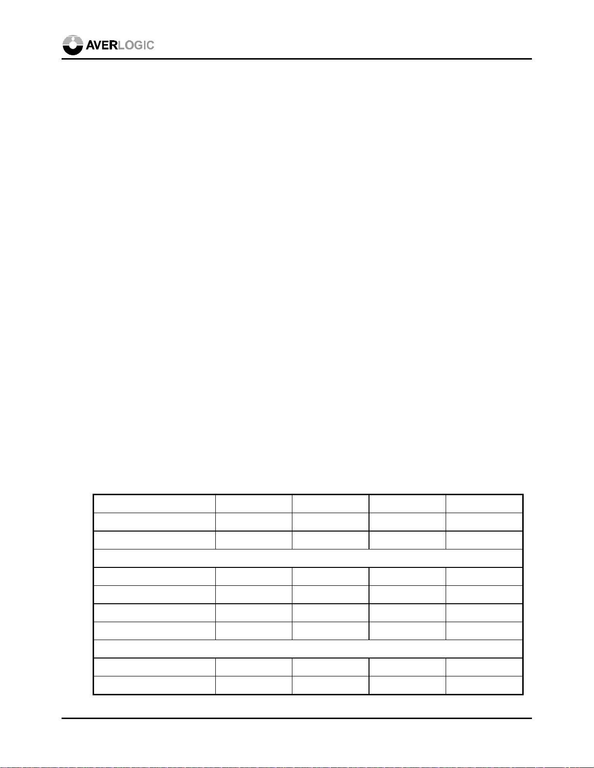
7.0 Electrical Characteristics
7.1 Recommended Operating Conditions
Parameter Min Max Unit
VDD Supply Voltage +3.0 +5.5 V
TAMB Ambient Operating Temperature 0 +70 °C
7.2 Characteristics
Parameter Test Conditions Min Max Unit
AL250
I
DD
Supply current 55 110 mA
P Power consumption 180 600 mW
V
Hi-level input voltage 0.7VDD VDD+0.5 V
IH
VIL Lo-level input voltage -0.5 +0.8 V
VOH Hi-level output voltage 2.4 VDD V
VOL Lo-level output voltage - 0.5 V
I
O
Output current, data -0.5V<VO<VDD+0.5 -2 2 mA
Output current, GHREF -0.5V<VO<VDD+0.5 -4 4 mA
Output current, GHS, GVS -0.5V<VO<VDD+0.5 -12 12 mA
I
LI
C
δ
CK2
t
iS
t
iH
t
r
Input leakage current - 1
Input pin capacitance - 8 PF
i
Duty factor (t
CK2H/tCK2
) 40 60 %
Input data set-up time 7 - ns
Input data hold time 3 - ns
Input rise time Vi = 0.6 to 2.6V - 7 ns
µA
t
t
C
t
t
f
dCK
oH
PD
Input fall time Vi = 2.6 to 0.6V - 7 ns
VCLK to VCLKx2 delay -1 +1 ns
Digital output load cap. 15 50 PF
L
Output hold time CL = 15pF 5 - ns
Propagation delay CL = 40pF - 15 ns
July 28, 1999 20
Page 21

The input and output timing diagrams are as follows:
tCK2
VCLKX2
AL250
VCLK
VDIN
VCLKX2
tdCK
tCK2H
tCK2L tf tr
tCK
trtf
tiS tiH
AL250-22 Input timing
tCK2
DO
tCK2H
tCK2L tf tr
tPD
toH
AL250-23 Output timing
July 28, 1999 21
Page 22

AL250
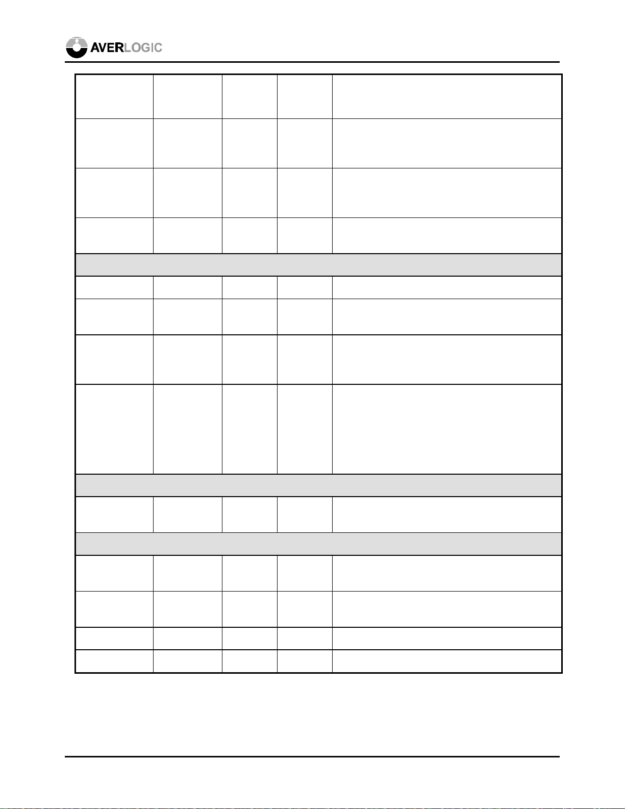
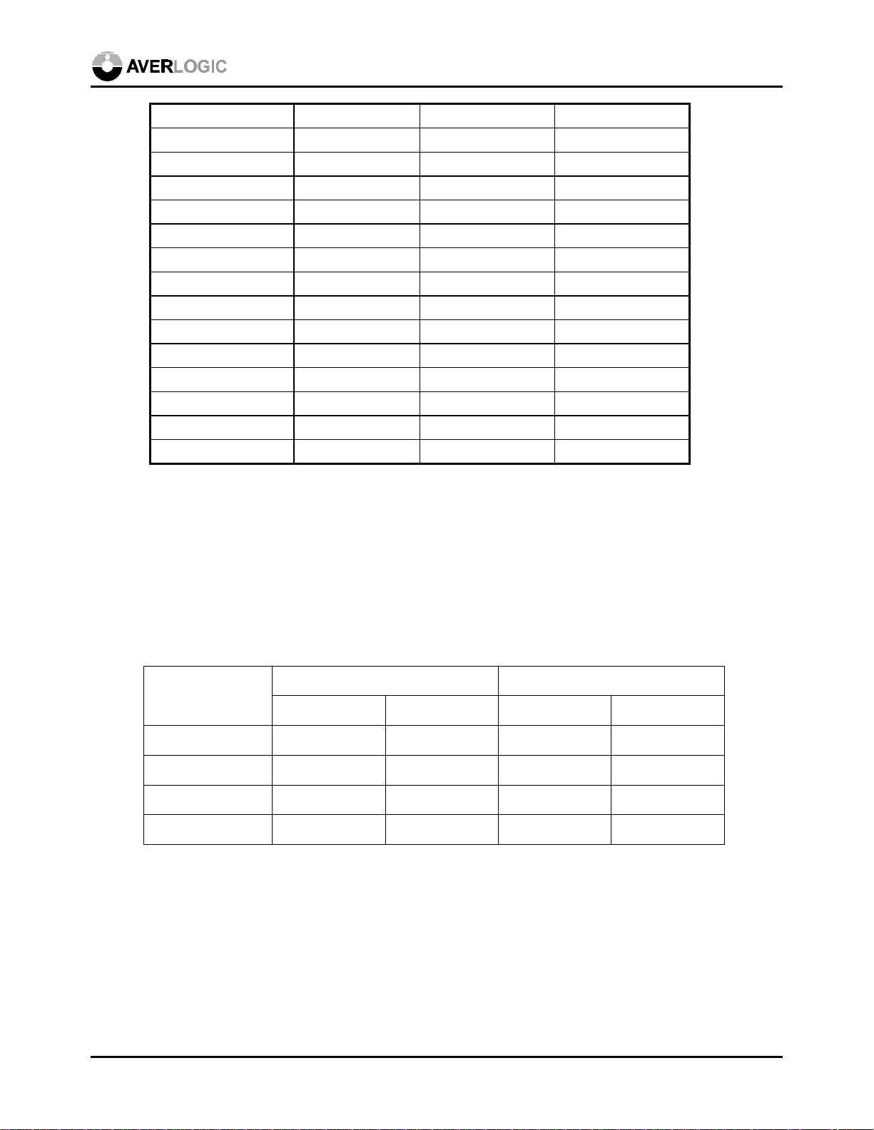
8.0 AL250/251 Register Definition
The AL250/251 is powered up to a default state depending on the hardware mode-setting pins.
Hardware configuration pins are disabled by setting SoftConfig (bit 4 of register 03h) to one, and
configurations are decided by the values of register 02h which is software programmable.
The following is the summary of the AL250/251 control registers
Register Addr. R/W Default Function
COMPANYID 00h R 46h Company ID
REVISION 01h R 00h Revision number
BOARDCONFIG 02h R/W ?? Board configuration
GENERAL 03h R/W 00h General control
FAMILY 04h R 25h Chip family number
CONTROL 08h R/W 00h Control register
STATUS 09h R ?? Status register
BORDERRED 0Ch R/W 00h Border color, red channel
BORDERGREEN 0Dh R/W 00h Border color, green channel
BORDERBLUE 0Eh R/W 00h Border color, blue channel
LUTOSDCONTROL 10h R/W 00h LUT/OSD control
LUTOSDINDEX 11h W 00h LUT/OSD index
12h Reserved
LUTOSDDATA 13h W 00h LUT/OSD data
OVERLAYCTRL 14h R/W 00h Overlay Effect Control
OVL1RED 15h R/W 00h Overlay color 1, red channel
OVL1GREEN 16h R/W 00h Overlay color 1, green channel
OVL1BLUE 17h R/W FFh Overlay color 1, blue channel
OVL2RED 18h R/W FFh Overlay color 2, red channel
OVL2GREEN 19h R/W FFh Overlay color 2, green channel
OVL2BLUE 1Ah R/W 00h Overlay color 2, blue channel
OVL3RED 1Bh R/W FFh Overlay color 3, red channel
OVL3GREEN 1Ch R/W 00h Overlay color 3, green channel
OVL3BLUE 1Dh R/W 00h Overlay color 3, blue channel
OSD1HSTART 1Eh R/W 00h On Screen Display bitmap 1 horizontal start
OSD2HSTART 1Fh R/W 00h On Screen Display bitmap 2 horizontal start
HDESTART 20h R/W 00h Horizontal capture start
HDEEND 21h R/W 00h Horizontal capture end
July 28, 1999 22
Page 23

AL250
HSYNCSTART 22h R/W 00h Horizontal sync. start
HSYNCEND 23h R/W 00h Horizontal sync. end
HTOTAL(1) 24h R/W 00h Horizontal total high, bit<10:3>
VDESTART 25h R/W 00h Vertical capture start
VDEEND 26h R/W 00h Vertical capture end
VSYNCSTART 27h R/W 00h Vertical sync. start
VSYNCEND 28h R/W 00h Vertical sync. end
HTOTAL(2) 29h R/W 00h Horizontal total low, bit<2:1>
TEST 2Ah R/W 00h Test register(Reserved)
HBORDERSTART 2Bh R/W 00h Horizontal border color start
HBORDEREND 2Ch R/W 00h Horizontal border color end
VBORDERSTART 2Dh R/W 00h Vertical border color start
VBORDEREND 2Eh R/W 00h Vertical border color end
OSDVSTART 2Fh R/W 00h On Screen Display bitmap 1 and 2 vertical start
8.1 Register Description
00h: Company ID (R) [COMPANYID]
CompanyId <7:0> Company ID (46h)
01h: Revision (R) [REVISION]
Revision <7:0> Revision number
02h: Board Configuration (R/W) [BOARDCONFIG]
If SoftConfig (Reg.#03h<4>) = 0, the hardware configuration pins values are read.
If SoftConfig (Reg.#03h<4>) = 1, the software configuration register values are read
STD <1:0> Input video standard
00 NTSC input
01 PAL input
10 Automatic standard detection
11 Reserved for analog testing
InType <2> Input video format
0 YUV422
1 RGB565
uvflip <3> if 1, flip UV
Square <4> 0 CCIR
1 Square pixel
03h: General (R/W) [GENERAL]
July 28, 1999 23
Page 24

<0> Reserved
<3:1> Reserved
SoftConfig <4> Enable configuration defined by software configuration register
<7:5> Reserved
04h: Chip Family (R) [FAMILY]
Family <7:0> 25h, AL250/251 series
08h: Control (R/W) [CONTROL]
<0> Reserved
InVsPol <1> Input vsync polarity
InHsPol <2> Input hsync polarity
Softtime <3> Enable H & V adjustment (register 20h to 29h)
OutHsPol <4> Output hsync polarity
OutVsPol <5> Output vsync polarity
OutFormat <7> Output video format
AL250
02h. Please refer to Reg.#02h
0 negative polarity
1 positive polarity
0 negative polarity
1 positive polarity
0 negative polarity
1 positive polarity
0 negative polarity
1 positive polarity
0 16-bit RGB 565
1 CCIR YUV422
09h: Chip Status (R) [STATUS]
PalDetected <0> PAL detected
VidVs <1> External vsync
HRef <2> External href
VidHs <3> External hsync
GVde <4> Internal gvde signal
OvlCtrl0 <5> External ovlctrl0
OvlCtrl1 <6> External ovlctrl1
Note:
If PalDetected is always 1, the input mode is PAL. If PalDetected is not always 1, then the input mode
is NTSC.
0Ch: Border Color Red (R/W) [BORDERRED]
BorderRed <7:0> Border color, red component
0Dh: Border Color Green (R/W) [BORDERGREEN]
BorderGreen <7:0> Border color, green component
0Eh: Border Color Blue (R/W) [BORDERBLUE]
July 28, 1999 24
Page 25

BorderBlue <7:0> Border color, blue component
10h: LUT/OSD Control (R/W) 0x10 [LUTOSDCONTROL]
LutOsdWSel <1:0> LUT/OSD table write select
00 enable LUT-red table write
01 enable LUT-green table write
10 enable LUT-blue table write
11 enable OSD (On Screen Display) bitmap write
RLutEn <2> LUT-red enable
0 bypass red LUT
1 enable red LUT
GLutEn <3> LUT-green enable
0 bypass green LUT
1 enable green LUT
BLutEn <4> LUT-blue enable
0 bypass blue LUT
1 enable blue LUT
BitMap1En <6> Bitmap 1 enable
0 hide bitmap 1
1 show bitmap 1
BitMap2En <7> Bitmap 2 enable
0 hide bitmap 2
1 show bitmap 2
AL250
11h: LUT/OSD Index (W) [LUTOSDINDEX]
LutOsdIndex <7:0> LUT/OSD index
13h: LUT/OSD Data (W) [LUTOSDDATA]
LutOsdData <7:0> LUT/OSD data
To program the contents of LUT/OSD, first set Reg.#10h, bit<1:0>, then repeat writing index value to
Reg.#11h, and data value to Reg.#13h.
14h: Overlay Control (R/W) [OVERLAYCTRL]
OvlLogic1 <1:0> Overlay logic operation between video and overlay color 1 when
overlay key = “01”
00 select overlay color 1
01 video AND overlay color 1
10 video OR overlay color 1
11 video XOR overlay color 1
OvlLogic2 <3:2> Overlay logic operation between video and overlay color 2 when
overlay key = “10”
00 select overlay color 2
01 video AND overlay color 2
10 video OR overlay color 2
11 video XOR overlay color 2
July 28, 1999 25
Page 26

OvlLogic3 <5:4> Overlay logic operation between video and overlay color 3 when
overlay key = “11”
00 select overlay color 3
01 video AND overlay color 3
10 video OR overlay color 3
11 video XOR overlay color 3
OvlLut <7> If 1, video will go through LUTs when ovlkey pins are “11” and
OvlLogic3 settings are ignored.
15h: Overlay Color 1 Red (R/W) [OVL1RED]
Overlay1Red <7:0> Overlay 1 color red component
16h: Overlay Color 1 Green (R/W) [OVL1GREEN]
Overlay1Green <7:0> Overlay 1 color green component
17h: Overlay Color 1 Blue (R/W) [OVL1BLUE]
Overlay1Blue <7:0> Overlay 1 color blue component
Default RGB value for overlay 1 is: (R, G, B) = (0, 0, 255), blue
18h: Overlay Color 2 Red (R/W) [OVL2RED]
Overlay2Red <7:0> Overlay 1 color red component
AL250
19h: Overlay Color 2 Green (R/W) [OVL2GREEN]
Overlay2Green <7:0> Overlay 1 color green component
1Ah: Overlay Color 2 Blue (R/W) [OVL2BLUE]
Overlay2Blue <7:0> Overlay 1 color blue component
Default RGB value for overlay 2 is: (R, G, B) = (255, 255, 0), yellow
1Bh: Overlay Color 3 Red (R/W) [OVL3RED]
Overlay3Red <7:0> Overlay 3 color red component
1Ch: Overlay Color 3 Green (R/W) [OVL3GREEN]
Overlay3Green <7:0> Overlay 3 color green component
1Dh: Overlay Color 3 Blue (R/W) [OVL3BLUE]
Overlay3Blue <7:0> Overlay 3 color blue component
Default RGB value for overlay 3 is: (R, G, B) = (255, 0, 0), red
1Eh: On-Screen Display 1 (OSD1) Horizontal Start (R/W) [OSD1HSTART]
Osd1HStart <7:3> On Screen Display bitmap 1 horizontal start. (unit: 64 pixels)
1Fh: On-Screen Display 2 (OSD2) Horizontal Start (R/W) [OSD2HSTART]
Osd2HStart <7:3> On Screen Display bitmap 2 horizontal start. (unit: 64 pixels)
2Fh: On Screen Display (OSD) Vertical Start (R/W) [OSDVSTART]
OsdVstart <7:4> On Screen Display bitmap 1 and 2 vertical start. (unit: 64 lines)
July 28, 1999 26
Page 27

AL250
MeshColor <1> Mesh color select
0 gray mesh
1 color 3 mesh
MeshEn <0> Mesh background enable
0 No mesh
1 Enable mesh background
To display the OSD correctly, make sure the horizontal start does not locate between horizontal sync
start and horizontal sync end, and vertical start does not locate between vertical sync start and vertical
sync end.
Reg.#20h to #29h define the video capture control timing.
20h: Horizontal Capture Start (R/W) [HDESTART]
HDEStart <7:0> Horizontal capture start. (unit: 8 pixels)
21h: Horizontal Capture End (R/W) [HDEEND]
HDEEnd <7:0> Horizontal capture end. (unit: 8 pixels)
22h: Horizontal Sync Start (R/W) [HSYNCSTART]
HSyncStart <7:0> Horizontal sync start. (unit: 8 pixels)
23h: Horizontal Sync End (R/W) [HSYNCEND]
HSyncEnd <7:0> Horizontal sync end. (unit: 8 pixels)
24h: Horizontal Total High (R/W) [HTOTAL1]
HTotal10_3 <7:0> Bit 10 to bit 3 of horizontal total
Bit 2 to bit 1 are defined in Reg.#29h<1:0>
25h: Vertical Capture Start (R/W) [VDESTART]
VDEStart <7:0> Vertical capture start. (unit: 4 lines)
26h: Vertical Capture End (R/W) [VDEEND]
VDEEnd <7:0> Vertical capture end. (unit: 4 lines)
27h: Vertical Sync Start (R/W) [VSYNCSTART]
VSyncStart <7:0> Vertical sync start. (unit: 4 lines)
28h: Vertical Sync End (R/W) [VSYNCEND]
VSyncEnd <7:0> Vertical sync end. (unit: 4 lines)
July 28, 1999 27
Page 28

29h: Horizontal Total Low (R/W) [HTOTAL2]
<7:2> Reserved
HTotal2_1 <1:0> Bit 2 to bit 1 of horizontal total, htotal bit 0 = 0
2Ah: Test (R/W) [TEST]
testIn <7> Feed RGB value from 0x15, 0x16, 0x17 registers to the input
testOut <6> Feed RGB value from 0x15, 0x16, 0x17 registers to the output
testOvl <5:4> 00, use hardware overlay key
01, set overlay key value to 01
10, set overlay key value to 10
11, set overlay key value to 11
<3:0> Reserved
2Bh: Horizontal Blank Start (R/W) [HBLANKSTART]
HBlankStart <7:0> Horizontal blanking start. (unit: 8 pixels)
2Ch: Horizontal Blank End (R/W) [HBLANKEND]
HBlankEnd <7:0> Horizontal blanking end. (unit: 8 pixels)
2Dh: Vertical Blank Start (R/W) [VBLANKSTART]
VBlankStart <7:0> Vertical blanking start. (unit: 4 lines)
AL250
2Eh: Vertical Blank End (R/W) [VBLANKEND]
VBlankStart <7:0> Vertical blanking end. (unit: 4 lines)
July 28, 1999 28
Page 29

AL250
9.0 Board Design and Layout Considerations
The AL250/251 contains both precision analog and high-speed digital circuitry. Noise coupling from
digital circuits to analog circuits may result in poor video quality. The layout should be optimized for
lowest noise on the power and ground planes by shielding the digital circuitry and providing good
decoupling.
It is recommended to place the AL250/251 chip close to the VGA output connector, and the video
decoder close to the analog video input connectors if applicable.
9.1 Grounding
Analog and digital circuits are separated within the AL250/251 chip. To minimize system noise and
prevent digital system noise from entering the analog portion, a common ground plane for all devices,
including the AL250/251 is recommended. All the connections to the ground plane should have very
short leads. The ground plane should be solid, not cross-hatched.
9.2 Power Planes and Power Supply Decoupling
The analog portion of the AL250/251 and any associated analog circuitry should have their own
power plane, referred to as the analog power plane (AVDD). The analog power plane should be
connected to the digital power plane (DVDD) at a single point through a low resistance ferrite bead.
The digital power plane should provide power to all digital logic on the PC board, and the analog
power plane should provide power to all of the AL250/251 analog power pins and relevant analog
circuitry.
Power supply connection pins should be individually decoupled. For best results, use 0.1µF ceramic
chip capacitors. Lead lengths should be minimized. The power pins should be connected to the bypass
capacitors before being connected to the power planes. 22µF capacitors should also be used between
the AL250/251 power planes and the ground planes to control low-frequency power ripple.
9.3 Digital Signal and Clock Interconnect
Digital signals to the AL250/251 should be isolated as much as possible from the analog outputs and
other analog circuitry. The high frequency clock reference or crystal should be handled carefully.
Jitter and noise on the clock will degrade the video performance. Keep the clock paths to the decoder
as short as possible to reduce noise pickup.
9.4 Analog Signal Interconnect
The AL250/251 should be located closely to the output connectors to minimize noise and reflections.
Keep the critical analog traces as short and wide (20~30 mil) as possible. Digital signals, especially
pixel clocks and data signals should not overlap any of the analog signal circuitry and should be kept
as far apart as possible. The AL250/251 and the decoder IC should have no inputs left floating.
July 28, 1999 29
Page 30

10.0 Mechanical Drawing
AL250: 20mm x 14mm 64-pin QFP package
AL250
July 28, 1999 30
Page 31

AL251: 20mm x 14mm 80-pin QFP package
AL250
July 28, 1999 31
Page 32

AL250
11.0 Power Consumption
The AL250/251 works at both 5V and 3.3V. The following table shows the current consumption of
the AL250/251 itself and that of the whole EVB with power supply at single 5V, or 5V and 3.3V
mixed (3.3V for the AL250/251 only).
+5V +3.3V for AL250
+5V for the rest
AL250/251 chip 92 mA (typ.) 55 mA (typ.)
AL250 EVB 280 mA (typ.) 140 mA (typ.)
Please be reminded that when lower power supply is used, the pull-down resistance to the RSET pin
has to be adjusted to compensate accordingly. The lower the supply voltage is, the lower the pulldown resistance has to be. The ideal resistance value can be achieved by adjusting the RGB output to
be 0.7V peak-to-peak or higher to obtain better output brightness and contrast.
For more information about the AL250/251 or other AverLogic products, please contact your local
authorized representatives, visit our website, or contact us directly.
July 28, 1999 32
Page 33

CONTACT INFORMATION
AverLogic Technologies, Inc.
6840 Via Del Oro
Suite 160
San Jose, CA 95119
USA
Tel : 1 408 361-0400
Fax : 1 408 361-0404
E-mail : sales@averlogic.com
URL : www.averlogic.com
 Loading...