

Page 1

AL128 Data Sheets
Page 2

Contents
AL128
1.0 Features ________________________ 3
2.0 Applications _____________________ 4
3.0 General Description _______________ 4
4.0 Pinout Diagram __________________ 5
5.0 Pin Definition and Description ______ 6
6.0 Functional Description ___________ 12
6.1 Input Interface ___________________ 12
6.1.1 24-bit RGB_______________________ 13
6.1.2 VAFC___________________________ 13
6.1.3 Feature Connector _________________ 14
6.1.4 Sampling (Pixel) Clock _____________ 14
6.2 Hardware and Software Control Modes
___________________________________ 15
6.3 Video Timing ____________________ 15
6.4 Supported Resolutions_____________ 17
6.5 Flicker Filter_____________________ 18
6.6 Overscan/Underscan Control _______ 18
9.0 Board Design and Layout
Considerations ______________________40
9.1 Grounding_______________________ 40
9.2 Power Planes _____________________ 40
9.3 Power Supply Decoupling __________ 40
9.4 Digital Signal and Clock Interconnect 40
9.5 Analog Signal Interconnect _________ 41
9.6 Component Placement _____________ 41
10.0 Mechanical Drawing _____________42
11.0 Power Consumption______________44
6.7 Pan and Position Control___________ 18
6.8 Zoom Feature ____________________ 18
6.9 Frame Buffer Management _________ 19
6.10 Digital Video Encoder ____________ 19
6.11 Push Button Interface/OSD________ 19
6.12 Memory Control Timing __________ 20
6.13 I2C Programming________________ 23
7.0 Electrical Characteristics__________ 26
7.1 Recommended Operating Conditions_ 26
7.2 Characteristics ___________________ 26
8.0 AL128 Register Definition_________ 27
8.1 Index of the Control Registers_______ 27
8.2 Control Register Description________ 28
8.3 AL128 Plug & Play Hardware Table _ 38
April 2, 1999 2
Page 3
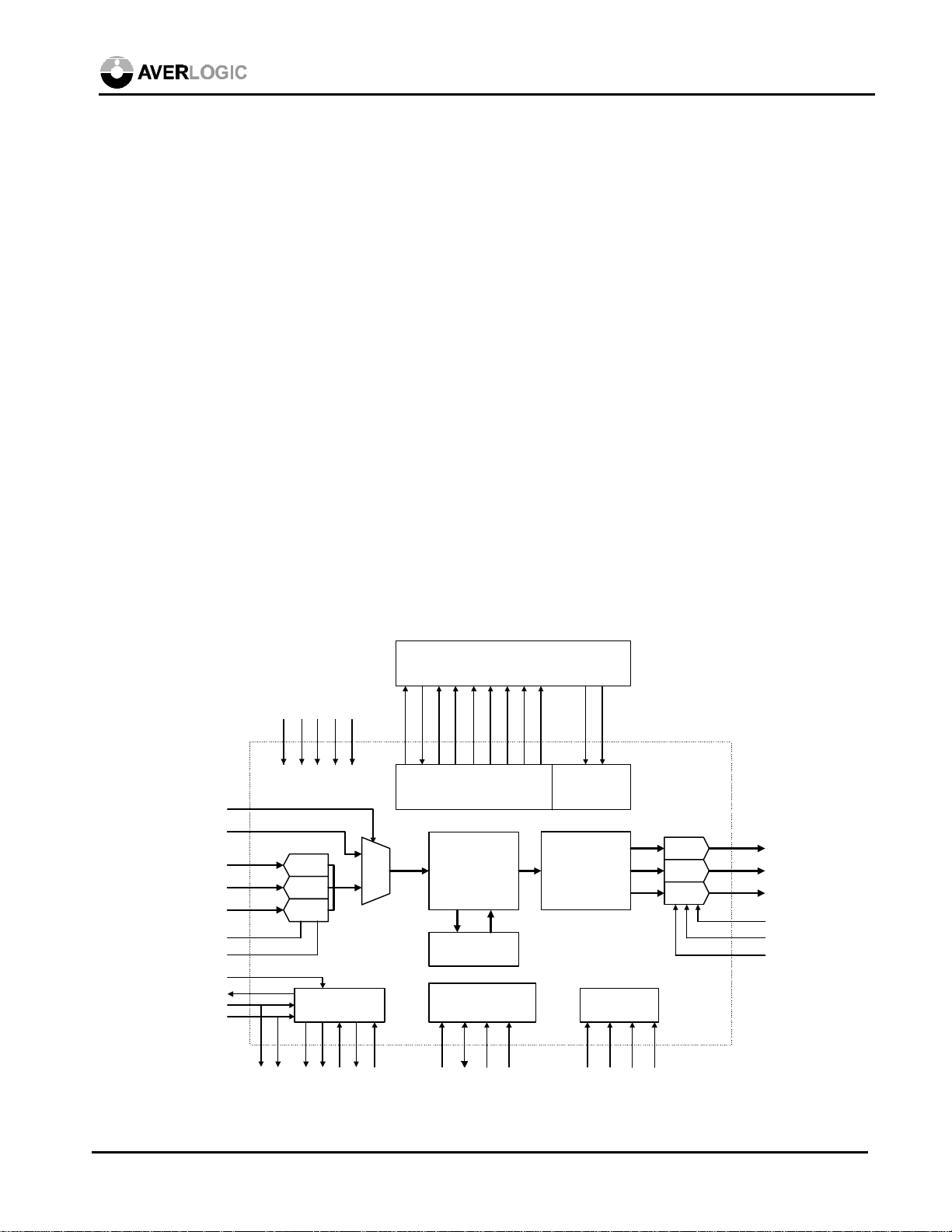
AL128 Plug and Play VGA to NTSC/PAL Converter
GHSOUT
GVSOUT
SELECT
I
1.0 Features
• Convert non-interlaced VGA or Macintosh
video into interlaced TV format (NTSC/PAL)
• Analog RGB output for SCART interface
• Highly integrated design with built-in
NTSC/PAL encoder, ADC, DAC and SRAM
• Broadcast TV quality
• High clarity 5-line anti-flicker filter
• 8 levels of sharpness control
• Plug and play with no need for software or
micro-controller
• Supports up to full 1024x768 VGA resolution
• Automatically supports scan rate from 50 Hz
up to 100 Hz
• Linear vertical and horizontal overscan/
underscan control
AL128
• Zoom and freeze controls
• Four-touch-button interface with on-screen-
menu (on TV) to control all key functions
• Horizontal and vertical position centering
control
• Optional digital 24-bit RGB/VAFC interface
for best quality
• Power down feature controlled by software or
hardware
• Full programmability via I2C interface
• Picture panning control
• Brightness control
• Built-in color bar
• Simultaneous display on PC and TV monitors
• Single 5-volt support
• Thin, small LQFP package for PCMCIA or
notebooks. 28x28 PQFP available upon request
ADEN
Digital R, G, B
VRT
VRB
GCLK
GHSDIV
GHSYNC
GVSYNC
Field Memory
RGB
PAL
/RESET/RESET
R
G
B
/PWRDN
8-bit
ADC
8-bit
ADC
8-bit
ADC
Generating
TVCLK
INTYPE
Timing
XIN1
XOUT1
MUX
XIN2
XOUT2
MD
MQ
Management
MWENL
MWRST
MWENH
Memory
Unit
Digital
Video
Processor
Video
Memory
I2C
2 C
Interface
SCL
SDA
MREN
MRRST
2
CADDR
2
MWCLK
C
I
MRCLK
Memory
Configuration
Digital
Encoder
MEMTYPE
MEMCONF
Setup
TV
Push Button
Interface
MENU
INC
DEC
9-bit
DAC
9-bit
DAC
9-bit
DAC
ACMP / R
AY / G
AC / B
RSET
VREF
COMP
AL128-01
April 2, 1999 3
Page 4

2.0 Applications
PC ready multimedia TV
TV output for laptop, network, entertainment PC
Net browser/set-top box
Internet TV
VGA add-on card with TV output
VGA to TV converter box
3.0 General Description
AL128
The AL128 PC to TV scan converter chip
accepts graphic data up to 1024x768
resolution from PC and Macintosh graphics
controllers and converts it into broadcastquality NTSC or PAL TV signals. In addition
to analog RGB, 24-bit digital RGB data can
be input to maintain the best video quality and
avoid noise problems. This new chip is pin-topin compatible with the AverLogic AL100 but
provides analog RGB output for SCART
implementation.
An integrated high-quality anti-flicker filter
(SmartFilter ) removes the unpleasant
flicker caused by the interlaced display of high
contrast graphics while maintaining the
original clarity and sharpness of informative
data such as natural pictures and text.
With 512Kbytes of memory, plug-and-play is
achieved by automatically detecting the scan
rate and resolution of the incoming graphic
signals without the use of software. With less
memory than other solutions on the market,
high resolution data is processed and stored by
using a complex and proprietary buffer
management system. No compromise is made
at all with video quality by using either
compression or sub-sampling algorithms.
The major functions of the AL128 can be
accessed using four push buttons combined
with the on-screen-menu feature, eliminating
the cost of a micro-controller and complex
control panel. The superior quality scaling
algorithm, which reduces the jagged-edge
artifacts from line dropping, can smoothly fit
graphics of 640x480 (up to 100 Hz) and
1024x768 (up to 75Hz) resolutions into the
visible region of the NTSC or PAL screen.
Both horizontal and vertical sizes can be
linearly adjusted. Additional features include
eight levels of flicker control using 5-line
filter, zoom control and picture freeze.
This highly integrated mix-signal chip,
packaged in 24mm x 24mm 160-pin LQFP
(low quad flat package), is powered by a
single 5-volt power supply. Power-down is
achieved by using either hardware or software
control.
The enhanced features and superior quality
make the AL128 very suitable for PC video to
TV conversion in PC ready multimedia TV’s,
scan converter boxes, VGA add-on cards,
Web TVs, or network / laptop PCs.
April 2, 1999 4
Page 5
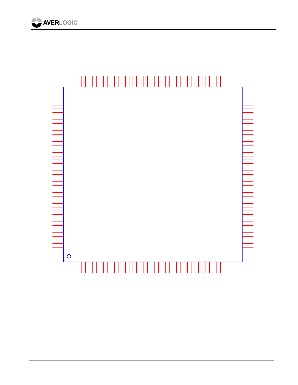
4.0 Pinout Diagram
120
119
118
117
116
115
114
113
112
111
110
109
108
107
106
105
104
103
102
101
100
AL128
99
98
97
96
95
94
93
92
91
90
89
88
87
86
85
84
83
82
81
121
122
123
124
125
126
127
128
129
130
131
132
133
134
135
136
137
138
139
140
141
142
143
144
145
146
147
148
149
150
151
152
153
154
155
156
157
158
159
160
BLUE5
BLUE4
VDD
BLUE3
BLUE2
BLUE1
BLUE0
ADGND
AB
ADVDD
ADVDD
AG
ADGND
VRT
VRB
ADGND
AR
ADVDD
VDD
GHSYNC
GVSYNC
GND
GCLK
VDD
GHSOUT
GHSDIV
GVSOUT
/PWRDN
/RESET
VDD
TVCLK
CLKTYPE
XOUT2
XIN2
GND
INTYPE1
INTYPE0
XOUT1
XIN1
GND
GND
BLUE6
BLUE7
RGBOUT
PAL
INC
GREEN0
GREEN1
GREEN2
DEC
SELECT
MENU
VDD
GREEN3
GREEN4
ADEN
VDD
TEST1
GREEN5
GREEN6
GREEN7
I2CADDR
SDA
I2C
GND
SCL
RED0
RED1
GND
TEST2
RED2
RED3
RED4
RED5
RED6
RED7
AL128
GND
TEST3
TEST4
TEST5
TEST6
TEST7
VDD
MQ0
TEST8
TEST9
MQ1
MQ2
VDD
TEST10
MQ3
MQ4
GND
GVSOUT2
TEST11
MQ5
MQ6
MQ7
TVVSYNC
TVHSYNC
GHSOUT2
GND
VDD
MD0
MD1
MD2
TVCSYNC
DAVDD
VREF
TEST12
MD3
MD4
GND
DAGND
AC/BOUT
MD5
MD6
MWENL
MWENH
MEMCONF0
MEMCONF1
MWCLK
MEMTYPE
MWRST
MRRST
MRCLK
DAVDD
DAVDD
DAGND
DAGND
AY/GOUT
MD7
VDD
GND
VDD
GND
MREN
MQ8
MQ9
MQ10
MQ11
VDD
MQ12
MQ13
MQ14
MQ15
GND
MD8
MD9
MD10
MD11
GND
MD12
MD13
MD14
MD15
VDD
COMP
RSET
ACMP/
ROUT
80
79
78
77
76
75
74
73
72
71
70
69
68
67
66
65
64
63
62
61
60
59
58
57
56
55
54
53
52
51
50
49
48
47
46
45
44
43
42
41
1
2
3
4
5
6
7
8
9
10
11
12
13
14
15
16
17
18
19
20
21
22
23
24
25
26
27
28
29
30
31
32
33
34
35
36
37
38
39
40
April 2, 1999 5
Page 6
5.0 Pin Definition and Description
Total pin count: 160 pins
Symbol Type Pin Description
/PWRDN in (CMOSd) 148 Power down enable (active low)
/RESET in (CMOSd) 149 Reset (active low)
AB in (0.7 V) 129 Analog Blue
AC/BOUT out (1/0.7 V p-p) 37 Analog chroma output or analog blue output
ACMP/ROUT out (1/0.7 V p-p) 41 Analog composite output or analog red output
ADEN in (CMOSd) 7 Internal ADC enable
0, internal ADC disable
1, internal ADC enable
AG in (0.7 V) 132 Analog Green
AL128
AR in (0.7 V) 137 Analog Red
AY/GOUT out (1/0.7 V p-p) 39 Analog luma output or analog green output
BLUE<7:0> in (CMOSd) 119-122, 124-
127
CLKTYPE in (CMOSd) 152 Clock Frequency
COMP in (0.1uF) 43 DAC Compensation pin, 0.1uF pull-up
DEC in (CMOSsd) 4 Decrement button
GCLK in (CMOS) 143 Graphic pixel clock
GHSDIV out (CMOS) 146 Graphic pixel clock divide by M signal for
GHSOUT out (TTL) 145 Graphic hsync output buffered from external
Graphic Blue input data
0 - 28.63636 MHz for NTSC,
35.46895 MHz for PAL
1 - 14.31818 MHz for NTSC,
17.734475 MHz for PAL
external PLL circuits.
VGA HSYNC
GHSOUT2 out (CMOS) 28 No Connection
GHSYNC in (CMOSd) 140 Graphic Hsync
GREEN<7:0> in (CMOSd) 109-112, 114-
117
Graphic Green input data
April 2, 1999 6
Page 7
GVSOUT out (TTL) 147 Graphic vsync output buffered from external
VGA VSYNC
GVSOUT2 out (CMOS) 27 Buffered graphic vsync output II.
GVSYNC in (CMOSd) 141 Graphic VSYNC
I2C in (CMOSd) 12 I2C/Vsync programming select
0 - enable VGA sync programming
1 - enable I2C programming
I2CADDR in (CMOSd) 11 I2C sub address
0 - write address = 88, read address = 89
1 - write address = 8C, read address = 8D
INC in (CMOSsd) 3 Increment button
INTYPE<1:0> in (CMOSd) 156,157 Graphic input type
00 - 24-bit RGB 01 - reserved
10 - feature connector
AL128
11 - VAFC
MD<15:0> out (CMOS) 47-50, 52-55,
80-83, 85-88
MEMCONF
in (CMOSd) 75,76 External memory configuration
<1:0>
Memory data to input of external field
memory.
00 – Reserved
01 – One-field memory capture
10 – Two-field memory capture
11 – Reserved
MEMTYPE in (CMOSd) 72 Memory type
0 - OKI MSM518221/222
1 – AverLogic AL422 or NEC µPD42280
MENU in (CMOSsd) 6 Menu button
MQ<15:0> in (CMOSd) 57-60, 62-65,
90-93, 95-98
Memory data from output of external field
memory.
MRCLK out (CMOS) 68 Memory Read Clock
MREN out (CMOS) 66 Memory Read Enable
MRRST out (CMOS) 69 Memory Read Reset
MWCLK out (CMOS) 73 Memory Write Clock
MWENH out (CMOS) 77 Memory High Byte Write Enable
April 2, 1999 7
Page 8
MWENL out (CMOS) 78 Memory Low Byte Write Enable
MWRST out (CMOS) 71 Memory Write Reset
PAL in (CMOSd) 2 NTSC/PAL select
0 - NTSC
1 - PAL
RED<7:0> in (CMOSd) 100-107 Graphic Red input data
RGBOUT in (CMOSd) 1 RGB/YC Composite output select
0 - ACMP, AY, AC
1 - R, G, B
RSET in 42 DAC Full scale current adjust, 82 ohm pull-
down for S-video and Composite output, 140
ohm pull-down for RGB output.
SCL in (CMOSsu) 13 I2C Clock
SDA in/out (CMOSsu) 10 I2C Data
AL128
SELECT in (CMOSsd) 5 Select button
TEST1~12 out (CMOS) 9, 15-18, 20-
Unused pins for factory test purpose only
23, 25,26,33
TVCSYNC out (CMOS) 32 TV composite sync
TVHSYNC out (CMOS) 30 TV horizontal sync
TVVSYNC out (CMOS) 31 TV vertical sync
TVCLK out (CMOS) 151 Clock output for graphic chip clock
VRB in (0 V) 135 ADC Bottom Voltage Reference
VREF in (1.23 V) 35 DAC Voltage Reference Input
VRT in 134 ADC Top Voltage Reference
XIN1/FIN1 in (CMOS) 159 Crystal Input/External Clock Input 1 for
NTSC
XIN2/FIN2 in (CMOS) 154 Crystal Input/External Clock Input 2 for PAL
XOUT1 out (CMOS) 158 Crystal Output 1 for NTSC
XOUT2 out (CMOS) 153 Crystal Output 2 for PAL
Power and Ground
VDD x 13 5V 8, 24, 46, 61,
70, 79, 89, 99,
113, 123, 139,
144, 150
Digital power
April 2, 1999 8
Page 9

AL128
GND x 14 14, 19, 29, 51,
56, 67, 74, 84,
94, 108, 118,
142, 155, 160
ADVDD x 3 5V 130,131,138 ADC power
ADGND x 3 128,133,136 ADC ground
DAVDD x 3 5V 34,44,45 DAC power
DAGND x 3 36,38,40 DAC ground
Digital ground
Remarks:
CMOSd: CMOS with internal pull-down
CMOSsd: CMOS with Schmitt trigger and internal pull-down
CMOSsu: CMOS with Schmitt trigger and internal pull-up
Pin list grouped by functionality
Symbol Pin Number
Graphic Interface
BLUE<7:0> 119-122, 124-127
GREEN<7:0> 109-112, 114-117
RED<7:0> 100-107
GHSYNC 140
GVSYNC 141
GCLK 143
GHSDIV 146
GHSOUT 145
GHSOUT2 28
GVSOUT 147
GVSOUT2 27
Field Memory Interface
MD<15:0> 47-50, 52-55, 80-83, 85-88
MQ<15:0> 57-60, 62-65, 90-93, 95-98
MWENH 77
April 2, 1999 9
Page 10
MWENL 78
MWRST 71
MREN 66
MRRST 69
MWCLK 73
MRCLK 68
TV Output
ACMP/ROUT 41
AY/GOUT 39
AC/BOUT 37
TVCSYNC 32
TVHSYNC 30
TVVSYNC 31
AL128
Clocks
XIN1/FIN1 159
XOUT1 158
XIN2/FIN2 154
XOUT2 153
TVCLK 151
User Interface
SCL 13
SDA 10
MENU 6
SELECT 5
INC 3
DEC 4
Mode select Pins
RGBOUT 1
PAL 2
INTYPE<1:0> 156,157
MEMCONF<1:0> 75,76
I2CADDR 11
April 2, 1999 10
Page 11
I2C 12
MEMTYPE 72
ADEN 7
CLKTYPE 152
/PWRDN 148
/RESET 149
D/A Converters
COMP 43
VREF 35
RSET 42
DAVDD x 3 34,44,45
DAGND x 3 36,38,40
A/D Converters
AL128
AR 137
AG 132
AB 129
VRT 134
VRB 135
ADVDD x 3 130,131,138
ADGND x 3 128,133,136
Test Pins
TEST1~12 9, 15-18, 20-23, 25, 26, 33
Digital Power
VDD x 13 8,24,46,61,70,79,89,99,113,123,139,144,150
GND x 14 14,19,29,51,56,67,74,84,94,108,118,142,155,160
April 2, 1999 11
Page 12
AL128
6.0 Functional Description
The AL128 accepts either analog RGB or digital RGB data. The analog RGB data is digitized by
three 50MHz 8-bit video A/D converters and is converted into 24-bit digital RGB data. For graphic
controllers with standard or proprietary digital RGB output such as a high-color feature connector,
VAFC, or flat panel interface, the optional 24-bit digital RGB interface provides a solution for
optimal video quality.
The 24-bit digital RGB is passed to the digital processing unit of the chip. This DSP unit performs
scan conversion operations and other digital signal processing such as flicker filtering, YUV filtering,
scaling and color space conversion in the digital domain. The processed video data is sent to the
digital TV encoder for converting into broadcast quality composite and S-video signals or original
RGB format, which are in turn converted by three 9-bit D/A converters into analog outputs.
Functions can be controlled by dedicated hardware pins as well as software. The I2C interface
provides full software programmability. The aforementioned hardware and software programmability
also applies to the power-down feature. Alternatively only four push buttons are required to control
the major functions such as sharpness, pan, zoom, brightness, color bar output and position centering
without the use of software or microcontroller.
6.1 Input Interface
RGB data and horizontal and vertical sync signals of the VGA controller are used as inputs. Analog
RGB data or 24-bit digital RGB data are both supported. The analog R, G, B signals are digitized
with three built-in 8-bit A/D converters. The voltage swing of VGA RGB signals is typically 0.7
volts. The VRT and VRB pins set the input voltage references of the A/D converters. When digital
RGB data is used as the input, the internal A/D converters can be disabled by setting pin ADEN low,
which may significantly reduce the power consumption.
Digital inputs for the AL128 can be either 24-bit RGB 888 or 16-bit RGB 565. RGB 565 can in turn
be in VAFC or feature connector format. The INTYPE pins of the AL128 have to be set correctly
to match the different applications.
INTYPE <1:0>
Pin 156, pin 157
0 0 24-bit RGB
0 1 Reserved
1 0 Feature connector (RGB565)
1 1 VAFC (RGB565)
Digital Graphic Input Type
April 2, 1999 12
Page 13
6.1.1 24-bit RGB
The digital 24-bit RGB can be pin-to-pin wired to RED<7:0>, GREEN<7:0> and BLUE<7:0> of
the AL128.
6.1.2 VAFC
The VAFC format (16-bit, RGB565, in 64k high color) carries red signals in D15~D11, green
signals in D10~D5, and blue signals in D4~D0.
There are two ways to implement VAFC interface. The first way is to set INTYPE as 11 to
accept VAFC format, then input the 16-bit RGB565 (64k high color) to GREEN<7:0> and
BLUE<7:0> of the AL128 as follows:
AL128
D15
D14
D13
D12
D11
D10
D9
D8
GREEN 7
GREEN 6
GREEN 5
GREEN 4
GREEN 3
GREEN 2
GREEN 1
GREEN 0
D7
D6
D5
D4
D3
D2
D1
D0
BLUE 7
BLUE 6
BLUE 5
BLUE 4
BLUE 3
BLUE 2
BLUE 1
BLUE 0
The other way is to keep INTYPE setting as 00 to accept 24-bit RGB888, but connect the inputs
to the higher bits of RED<7:0>, GREEN<7:0> and BLUE<7:0> of the AL128 as follows. The
unused pins can be grounded.
D15
D14
D13
D12
D11
D10
D9
D8
D7
D6
D5
D4
D3
D2
D1
D0
RED 7
RED 6
RED 5
RED 4
RED 3
GREEN 7
GREEN 6
GREEN 5
GREEN 4
GREEN 3
GREEN 2
BLUE 7
BLUE 6
BLUE 5
BLUE 4
BLUE 3
April 2, 1999 13
Page 14
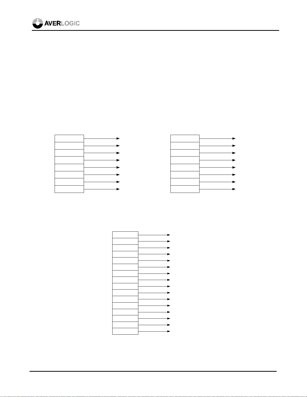
6.1.3 Feature Connector
The definition of the data bits of the feature connector is same as that of the VAFC, i.e.,
D15~D11 represent red signals. D10~D5 green signals, and D4~D0 blue signals. However, since
the feature connector uses 8-bit interface, the two bytes of data must be received within one
pixel/graphic clock (GCLK). The solution is: one byte at the rising edge and one byte at the
falling edge of GCLK as follows:
AL128
DATA
D7~D0 D15~D8 D7~D0 D7~D0D15~D8
GCLK
The eight-bit data is wired to BLUE<7:0> of the AL128 as follows:
D7
D6
D5
D4
D3
D2
D1
D0
D15
D14
D13
D12
D11
D10
D9
D8
BLUE 7
BLUE 6
BLUE 5
BLUE 4
BLUE 3
BLUE 2
BLUE 1
BLUE 0
6.1.4 Sampling (Pixel) Clock
The sampling clock for the RGB data can come directly from the graphic pixel clock when this is
available. For external box applications where the graphic pixel clock is not available, the clock
is recovered from the VGA horizontal sync with an external PLL clock chip such as ICS
AV9173. The phase reference signal of the PLL clock chip is generated by the divide-by-M
circuitry of the AL128. The AL128 automatically sets the M divider value, which determines the
sampling frequency for the A/D converter according to the detected resolution of the incoming
graphic data.
April 2, 1999 14
Page 15

AL128
6.2 Hardware and Software Control Modes
The AL128 is powered up to a default state depending on the hardware mode-setting pins. Eight of
these hardware configuration pins are disabled by setting SoftConfig (bit 4 of register 03h) to one,
and configurations are decided by the values of register 0x02, programmable by software.
By default, AL128 major functions can be controlled by On Screen Display Menu (OSDM) push
buttons. The registers related to these functions have no effect on those On Screen Display Menu
functions unless DisButton (bit 3 of register 03h) is set to one. When this bit is set to one, the
external OSDM push buttons are deactivated and those functions are controlled by software
programming. The following table lists the functions that can be controlled by either push buttons or
software programming, and their corresponding registers.
Function Register Name Register Index
Sharpness VFltMode 33h<2:0>
Zoom Zoom
ZoomEn
Pan GinHStartDlt
GinVStartDlt
GinHStZoomDlt
GinVStZoomDlt
20h<1:0>
20h<7>
21h<7:0>
22h<7:0>
2Bh<6:0>
2Ch<6:0>
Underscan SoftUdScan 33h<6>
Position TvHStartDlt
TvVStartDlt
52h<7:0>
51h<7:0>
Brightness TvBright 50h<4:3>
Color Bar ColorBar 50h<1>
Details about the programming can be found in the Register Definition Section.
6.3 Video Timing
Although the AL128 is designed to be plug-&-play, it is programmable to meet special requirements.
This is especially advantageous when AL422 is used as field memory since larger memory capacity
means higher sampling resolution.
Horizontal capture and display timing is as follows:
April 2, 1999 15
Page 16

AL128
VGA Input
HSYNC
Default Capture Start
H-display Delta (Reg # 52h)
TV Output
Default Horizontal
Display Start
H total (Reg # 28h)
H Pan Delta (Reg # 21h), (Reg # 2Bh for Zoom)
H Capture Size (Reg # 23h)
* Scaled up ratio defined in Reg # 27h
Horizontal Display Size (Horizontal
Active Region Shown on TV)
TVHSYNC
Vertical capture and display timing is as follows:
Al128-16 Timing_horizontal
April 2, 1999 16
Page 17

AL128
VGA Input
VSYNC
Default V-Capture Start
TV Output
TVVSYNC
V-total (Reg # 43h)
Source Vertical Size (Reg# 24h)
V-pan Delta (Reg #22h), (Reg #2Ch for Zoom)
* Ratio defined in Reg # 26h
(see H/W table)
Down-Sample Vertical
Size (Reg #25h)
V-display Delta
(Reg #51h)
Default Vertical Display Start (see H/W table)
Al128-17 Timing_vertical
Details about register programming can be found in the Register Definition Section. Typical values
of the parameters for using AL128 with AL422 can be found in the AL128 Application Notes
Supplement.
6.4 Supported Resolutions
The resolutions that are automatically supported without any software are 640x400, 640x480 and
800x600. Other resolutions, such as 1024x768 full screen, are also supported through software
programming. Scan rates up to 100 Hz are supported for 640x480 resolution, up to 85 Hz for
800x600 resolution, and up to 75 Hz for 1024x768 resolution.
April 2, 1999 17
Page 18

AL128
6.5 Flicker Filter
The AL128 chip performs 5 line flicker filtering to reduce the flicker due to interlaced display of high
contrast lines. Eight levels of flicker reduction, as well as sharpness adjustment, are provided to
control the picture quality.
Proprietary dynamic filtering (SmartFilter ) is applied to retain the original PC video resolution and
sharpness while removing the flickering effect. The hardware intelligently detects which parts of the
screen are natural picture and which are text whose clarity needs to be retained. One out of 45
different filters is selected and applied dynamically for each single pixel based on the statistics of its
surrounding pixels. The criteria of which filter to choose from is based on a model derived from the
ensemble of psychophysical experiments based on human eye responses to the flicker of different
picture types.
6.6 Overscan/Underscan Control
Televisions normally overscan, meaning that the border of the picture is outside the visible area of
the TV screen. To program the AL128 from Overscan to Underscan, reduce the horizontal display
width and vertical display height, and increase the H-display delta and V-display delta. For
underscan to overscan, reverse the process. The capture-related registers may need to be
programmed for optimization.
The AL128 linearly scales the input picture into the visible part of a TV’s screen. Digital filtering
techniques are applied to remove the scaling artifacts.
6.7 Pan and Position Control
The panning feature selects the portion of the graphic picture to be displayed on the TV screen.
When in zoom mode, the visible screen can be progressively panned to any area of the virtual screen.
To pan the display, change the values of H-pan delta (Reg. #21h, #26h) and V-pan delta (Reg. #22h,
2Ch). To pan in zoom mode, #2Bh and #2Ch may also need to be programmed.
Position control is used to center the video on the TV screen. To position the display, change the
values of H-display delta (Reg. #52h) and V-display delta (Reg. #51h).
6.8 Zoom Feature
AL128 performs 2x zoom in both horizontal and vertical directions. This can be used with panning,
or activated by jumping to any given quadrant via use of the push buttons or software.
April 2, 1999 18
Page 19

AL128
To zoom, use register #20h to enable it, and then use #2Bh and #2Ch to position it.
6.9 Frame Buffer Management
Only one half Mbytes of field memory are needed to achieve 24-bit video quality and full resolution
scan conversion for either NTSC or PAL. Field memory supported is AverLogic AL422, NEC
µPD42280 and OKI MSM518221/222. With less memory than other solutions on the market, high
resolution data is processed and stored by using a complex and proprietary frame buffer management
system. There is no compromise with video quality by using either compression or sub-sampling
algorithms. Special care is taken in the design so that there is no tearing effect (feathered edge) when
playing back moving video sequences such as MPEG I or MPEG II.
To take advantage of the high capacity of the AL422, please review the AL128 Application Notes
Supplement for details.
6.10 Digital Video Encoder
The digital video encoder inputs the digital color-space and scan-rate converted video data and
output broadcast quality NTSC and PAL signals. The color sub-carrier is generated by a four times
over-sampling clock, which greatly simplifies external analog smoothing filter design. Eight times
over-sampling mode is also available by software control. The modulated digital signals are
converted to analog levels by three 9-bit D/A converters. Composite and S-video signals are output
simultaneously. Interlaced RGB output can also be provided.
6.11 Push Button Interface/OSD
The push button interface is used with the on-screen-display menu. There are four buttons: menu,
select, increment and decrement. Functions controlled by these push buttons are pan, zoom, position
centering, brightness, underscan, color bar and sharpness.
The AL128 EVB provides a user-friendly on-screen control with four push buttons, [Menu],
[Select], [<] and [>], for end users to control the major functions of the AL128. There are eight onscreen control functions, which are:
Sharpness Panning Positioning Color bar
Zoom Over/underscan Brightness Home settings
April 2, 1999 19
Page 20

AL128
• To pop up the on screen menu, press the [Menu] button.
• To select a control function, use the [<] or [>] button to scroll to it, then press the
[Select] button.
• After selecting a control function, use the [Select], [<] or [>] button to adjust the control
effects.
• To exit the on screen menu, press [Menu] again.
6.12 Memory Control Timing
The AL128 uses FIFO frame buffers such as the AL422 for scan rate conversion. The input analog
RGB signals are digitized at the regenerated GCLK speed. The captured and filtered digital data is
written to the FIFO’s at a slower speed by using MWENH and MWENL to reduce the bandwidth
while the MWCK is maintained at the same speed as GCLK (with a slight phase difference). The
enable duty cycle of the MWENH and the MWENL is programmable by controlling register #25h, as
long as the captured data volume does not exceed the FIFO capacity. The MWENH controls luma
data write enable; the MWENL controls chroma data write enable. After the whole frame data is
written, the WRRST is applied right before the next input frame is to be captured to reset the write
pointer back to zero.
The following drawing shows the graphic sync signals and FIFO control write timing:
April 2, 1999 20
Page 21

VSYNC
MWRST
VSYNC
MWRST
HSYNC
MWENH
MWENL
AL128
SYNC Back porchFront porch Active lines
MWRST
HSYNC
MWENH
MWENL
GHSDIV
(for PLL)
HSYNC
MWENL
(Chroma)
MWENH
(Luma)
32
cycles
SYNC
Back porch
Active pixels
Front
porch
GCLK
AL128-26 FIFO control VGA timing
April 2, 1999 21
Page 22

AL128
The read clock RCLK is either 14.318MHz for NTSC or 17.734MHz for PAL. Not every single
pixel of input data is read so that the bandwidth may fit the lower TV resolution, and this is
controlled by various enable duty cycles of the REN. PAL has a higher enable duty cycle than NTSC
because of its higher resolution. MRRST is applied right before the next valid output field to reset
the read pointer back to zero.
The following drawing shows the TV sync signals and FIFO control read timing:
RCK
REN
REN
TVHSYNC
CVBS
TVHSYNC
MRRST
TVVSYNC
MRRST
Front porch Back porch
SYNC Back porchFront porch Active lines
TVVSYNC
AL128-27 FIFO control TV timing
April 2, 1999 22
Page 23

AL128
6.13 I2C Programming
The AL100/110/128 I2C programming interface is slightly different from the Philips standard (same
write cycles but different read cycles). The I2C interface consists of the SCL (clock) and SDA (data)
signals. Data can be written to or read from the AL100/110/128. For both read and write, each byte
is transferred MSB first, and the SDA data bit is valid when the SCL is pulled high.
The read/write command format is as follows:
Write: <S> <Write SA> <A> <Register Index> <A> <Data> <A> <P>
Read: <S> <Read SA> <A> <Register Index> <A> <Data> <NA> <P>
Following are the details:
<S>:
Start signal
SCL SDA
High High
High Low
The Start signal is HIGH to LOW transition on the
SDA line when SCL is HIGH.
SDA
Data bit [1] or NA
SCL
<WRITE SA>:
Write Slave Address: 88h or 8Ch
<READ SA>:
Read Slave Address: 89h or 8Dh
<REGISTER INDEX>:
Value of the AL100/110/128 register index.
<A>:
Acknowledge stage
The acknowledge-related clock pulse is generated by
the host (master). The host releases the SDA line
(HIGH) for the AL100/110/128 (slave) to pull down
the SDA line during the acknowledge clock pulse.
<NA>:
Not Acknowledge stage
The acknowledge-related clock pulse is generated by
the host (master). The host releases the SDA line
SDA
Data bit [0] or A
SCL
SDA
START bit [S]
SCL
STOP bit [P]
SCL
SDA
Not significant
SCL
AL250-15 I2C drawing
April 2, 1999 23
Page 24

AL128
Start
Slave addr = 88h
Ack
Ack
Ack
Stop
Index = 0Fh
Data = F0h
NAck
(HIGH) during the acknowledge clock pulse, but the AL100/110/128 does not pull it down during
this stage.
<DATA>:
Data byte write to or read from the register index.
In read operation, the host must release the SDA line (high) before the first clock pulse is
transmitted to the AL100/110/128.
<P>:
Stop signal
SCL SDA
High Low
High High
The Stop signal is LOW to HIGH transition on the SDA line when SCL is HIGH.
Suppose data F0h is to be written to register 0Fh using write slave address 88h, the timing is as
follows (same as the Philips standard):
SDA
SCL
AL128-24 I2C Write timing
Suppose data is to be read from register 55h using read slave address 89h, the timing is as follows:
Slave addr = 89h Ack
StopData read cycle
SDA
SCL
April 2, 1999 24
Page 25

AL128
Start
Ack
Read slave addr = 59h
NAck
Stop
In comparison, reading data from register 55h using slave address 59h with Philips standard would
be as follows:
SDA
SCL
AckIndex = 55h
AL250-25 I2C Read timing
Data read cycle
April 2, 1999 25
Page 26

7.0 Electrical Characteristics
Parameter Min Unit
VDD +3.8 +5.5
TAMB Ambient Operating Temperature +70
Parameter Test Conditions Max Unit
AL128
I
Supply current 230 350 mA
DD
P Power consumption 875 1925 mW
V
Hi-level input voltage 0.7VDD VDD+0.5 V
IH
VIL Lo-level input voltage -0.5 +0.8 V
VOH Hi-level output voltage 2.4 VDD V
VOL Lo-level output voltage - 0.5 V
I
C
t
t
C
t
t
t
t
Input leakage current - 1
LI
Input pin capacitance - 8 PF
i
Input data set-up time 10 - ns
SU
Input data hold time 3 - ns
HD
Digital output load cap. 15 50 PF
L
Output hold time CL = 15pF 5 - ns
OH
Propagation delay CL = 40pF - 15 ns
PD
Output rise time Vi = 0.6 to 2.6V 3 7 ns
r
Output fall time Vi = 2.6 to 0.6V 3 7 ns
f
µA
26
Page 27

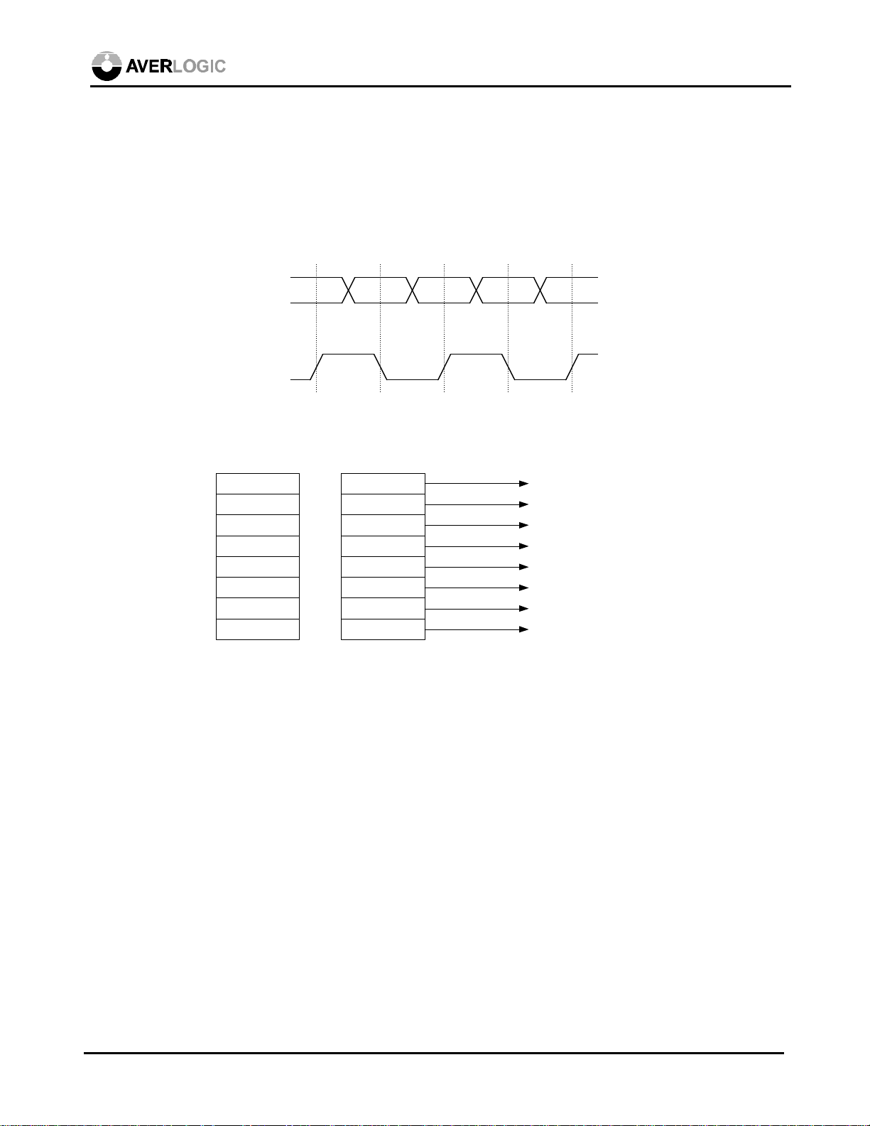
8.0 AL128 Register Definition
8.1 Index of the Control Registers
Register Index Function
Configuration
COMPANYID 00h Company ID number
REVISION 01h Revision number
BOARDCONFIG 02h Board configuration
GENERAL 03h General control
VERSION 04h Chip family number
Push Button Interface
SOFTBUTTON 18h Software button I
AL128
BUTTONSTATUS 19h Software button II
Graphic Input
GRAPHCTRL 20h Graphic control
GINHSTARTDLT 21h Delta of horizontal start
GINVSTARTDLT 22h Delta of vertical start
GINCAPHSIZE 23h Horizontal capture size
GINYSIZE 24h Source picture vertical size
CAPVSIZE 25h Destination picture vertical size
CAPVRATIO 26h Vertical scale ratio
DSPHRATIO 27h Horizontal scale ratio
PLLDIVIDER 28h PLL clock divider
GINHSTZOOMDLT 2Bh Delta of horizontal start in zoom mode
GINVSTZOOMDLT 2Ch Delta of vertical start in zoom mode
GRAPHDP 33h Graphic data processing control
40h Reserved (for assisting memory control)
Read Only Status Registers
HWCONFIG 41h Hardware configuration status
GINHTOTAL 42h Detected horizontal total
April 2, 1999 27
Page 28

GINVTOTAL 43h Detected vertical total
SCANRATE 44h Detected scan rate
TVSTATUS 45h Vertical position status
Encoder
ENCODERCTRL 50h Encoder control
TVVSTARTDLT 51h Delta of vertical display start
TVHSTARTDLT 52h Delta of horizontal display start
CAPINV 53h Capture control
Miscellaneous
MCAPVRATIO 71h M of vertical capture ratio value: N/M
NCAPVRATIO 72h N of vertical capture ratio value: N/M
CHROMABYPASS 73h Chroma filter bypass control
AL128
8.2 Control Register Description
00h: Company ID (R) [COMPANYID]
CompanyId <7:0> Company ID (0x46)
01h: Revision (R) [REVISION]
Revision <7:0> 00000001, Revision ID numbers
02h: Board Configuration (R/W) [BOARDCONFIG]
InType <1:0> Graphic input data format
00 Digital RGB 888
01 Reserved
10 Feature connector
11 VAFC
MemConf <3:2> External memory configuration
00 No external memory used
01 One-field memory capture
Only one field of video data is stored in the field
memory. This proprietary design increases the resolution
with limited 512kB memory (thus bringing better output
quality), but does not work when the input refresh rate is
April 2, 1999 28
Page 29

less than 66Hz for NTSC or 55Hz for PAL, or when
freeze control is used.
10 Two-field memory capture
Both odd and even fields of video data are stored in the
field memory. When the AL422 is used as the field
memory, there is enough capacity at all times so this
mode is suggested for programming simplicity.
11 Reserved
MemType <4> Memory Type
0 Oki field memory
1 NEC field memory
Pal <5> PAL/NTSC select
0 NTSC
1 PAL
F4sc <6> 0 Use 8 times SC sampling clock as TV clock
1 Use 4 times SC sampling clock as TV clock
RgbOut <7> 0 Composite and S-video output
1 RGB output
Settings of this register are enabled only when software programming is turned on by
writing 18h to Reg.#03h.
AL128
03h: General (R/W) [GENERAL]
PwrDown <0> Power down the chip if set to 1.
<2:1> Reserved
DisButton <3> Disable touch button function; use I2C/Vsync interface to
program the chip. This bit has to be turned on to enable all
the functions marked as ** xxx **.
SoftConfig <4> Enable configuration defined by software configuration
registers 0x02.
Reserved <7:5>
To use software programming properly, read the value of Reg.#41h (hardware
configuration) and write it to Reg.#02h. Then write value 18h to Reg.#03h.
04h: Chip Family (R) [VERSION]
Family <7:0> 00000000, AL100 series
Push-Button Interface
18h: Push Button Value (R/W): [SOFTBUTTON]
April 2, 1999 29
Page 30

<0> Reserved
<1> Reserved
<3:2> Reserved
ValuePtr <7:4> Number of on-screen-display white rectangle bar, to indicate
the level of strength. Works only when Reg.#19h <1> is
turned on.
19h: Push Button Status (R/W): [BUTTONSTATUS]
DspMenu <0> Enable display of on-screen-display menu icons
DspValue <1> Enable display of on-screen-display function icons
DspLeftR <2> Enable display of on-screen-display left-right icon
DspUpDn <3> Enable display of on-screen-display up-down icon
FuncPtr <6:4> Current function icon selected and highlighted.
000: sharpness function icon
001: zoom function icon
010: pan function icon
011: underscan/overscan function icon
100: position function icon
101: brightness function icon
110: color bar function icon
111: home function icon
<7> Reserved
AL128
Graphic Input Block
20h: Graphics Control Register (R/W) [GRAPHCTRL]
Zoom <1:0> zoomed quadrant ** zoom **
00 Zoom quadrant 0
01 Zoom quadrant 1
10 Zoom quadrant 2
11 Zoom quadrant 3
Meaningful only when ZoomEn = 1.
It is recommended not to set these bits when S/W mode is
enabled. Instead, use reg#2Bh and reg#2Ch to control the
zoomed video visible area.
Vga555 <2> VGA VAFC/feature connector 555/565 format select
0: 565 format
1: 555 format
April 2, 1999 30
Page 31

<3> Reserved
<4> Reserved
<5> Reserved
<6> Reserved
ZoomEn <7> Zoom enable ** zoom **
Set to 0 when in basic mode.
21h: Delta of Horizontal Start (R/W) [GINHSTARTDLT]
GinHStartDlt <7:0> Delta of default horizontal capture start position. (unit: 8
pixels) ** X Pan **
This register does not apply to zoom mode.
The actual horizontal capture start position is defined as:
(default horizontal capture start position) + (GinHStartDlt * 8).
The value of GinHStartDlt is signed, and its value is between –128 and 127.
Please refer to Section 8.3, AL128 Plug & Play Hardware Table for the default horizontal
capture start positions.
AL128
22h: Delta of Vertical Start (R/W) [GINVSTARTDLT]
GinVStartDlt <7:0> Bit-9 to bit-2 of GinVStartDlt; bit 1,0 are defined in Register
0x26. (Unit: one line) ** Y Pan **
This register does not apply to zoom mode.
The actual vertical capture start position is defined as:
(default vertical capture start position) + (GinVStartDlt * 4).
The value of GinVStartDlt is signed, and its value is between –128 and 127.
Please refer Section 8.3, AL128 Plug & Play Hardware Table for the default vertical
capture start positions.
23h: Horizontal Capture Size (R/W) [GINCAPHSIZE]
GinCapHSize <6:0> Horizontal capture size (Unit: 16 pixels)
SoftCapHSize <7> Override default H capture size value and use GinCapHSize
if set to 1.
This register defines the number of pixels of each valid horizontal line, which length is
defined by reg#22h (zoom off) or reg#2Ch (zoom on). Only the active horizontal lines are
captured, and the range is defined by reg#24h and reg#25h.
The actual horizontal capture size is defined as: GinCapHSize * 16.
The starting capture position is defined by reg#21h (zoom off) or reg#2Bh (zoom on).
The destination total displayed active pixels is defined as:
GinCapHSize * 16 * (scale-up ratio defined in reg#27h)
Please also refer to Section 6.3 Video Timing for better understanding.
April 2, 1999 31
Page 32

Make sure that:
(GinCapHSize * 16) <= 800(AL100/128 built-in line buffer size)
(GinCapHSize * 16) <= (reg#28h<6:0> * 16)
For one-field memory configuration, the value of (GinCapHSize * 16) * (reg#25h<6:0> *
8) * 2 must be less or equal to the total field memory size on board.
For two-field memory configuration, the value of (GinCapHSize * 16) * (reg#25h<6:0> *
8) * 2 * 2 must be less or equal to the total field memory size on board.
24h: Source Vertical Size (R/W) [GINVSIZE]
GinVSize <6:0> Vertical size of graphic input (unit: 8 lines)
SoftVSize <7> Override hardware detected V size value and use GinVSize
if set to 1.
This register defines the total number of input lines scanned, which starting position is
defined by reg#22h (zoom off) or reg#2Bh (zoom on).
The scanned input lines are scaled (down-sampled), filtered and captured into field
memory. The destination down-sampled size is defined in reg#25h.
The actual vertical source size is defined as: GinVSize * 8.
The starting position to scan input lines is defined by reg#22h (zoom off) or reg#2Bh
(zoom on).
See reg#26h for more description.
Please also refer to Section 6.3 Video Timing for better understanding
AL128
25h: Down-sampled Vertical Size (destination) [CAPVSIZE] (R/W)
CapVSize <6:0> (unit: 8 lines)
CapVSizeEn <7> enable software vertical size
This register defines the total number of scaled (down-sampled) and filtered video lines
captured into the field memory. The actual number is defined as: CapVSize * 8.
For one-field memory configuration, the value of (reg#23h<6:0> * 16) * (CapVSize * 8) *
2 must be less or equal to the total field memory size on board.
For two-field memory configuration, the value of (reg#23h<6:0> * 16) * (CapVSize * 8)
* 2 * 2 must be less or equal to the total field memory size on board.
See reg. #26h for more description
Please also refer to Section 6.3 Video Timing for better understanding
26h: Y Downscale Ratio [CAPVRATIO] (R/W)
CapVRatio <3:0> 0000 No line drop
0001 Drop 3 lines out of 10 lines
xxxx (from 0010 to 1110): drop one line for every
xxxx+1 lines
1111 vertical scale ratio defined as N/M
April 2, 1999 32
Page 33

N is defined at reg.#72h<5:0>
M is defined at reg.#71h<5:0>
CapVRatioEn <4> 0: Hardware default vertical scale ratio used for vertical
scaling.
1: Software vertical down-scale ratio CapVRatio used.
<5> Reserved
GinVStartDlt <7:6> bit 1,0 of 10-bit GinVStartDlt. Used with Reg 0x22
The relationship between registers #24h, #25h and #26h is that Reg. #25h<6:0>
approximately equals to Reg. #24h<6:0> * (Vertical scale ratio define in Reg. #26h)
Please also refer to Section 6.3 Video Timing for better understanding
27h: Horizontal Scale Ratio [DSPHRATIO] (R/W)
DspHRatio <5:0> Software horizontal scale ratio.
The value is ((HSRC/HDST) x 256 – 128) / 2
HSRC is horizontal capture size defined in reg. #23h
HDST is horizontal display active size.
The default overscan HDST for NTSC is 752; PAL is 954
The default underscan HDST for NTSC is 656; PAL is 800
The pixel total for 910x525 for NTSC, 1126x615 for PAL
The suggested HDST in zoom mode is 736~836 (NTSC)
and 800~1203 (PAL). Please review the S.5.2 and S.5.3
sections of the AL128 Application Notes (and find the DspH
value in different input modes) for details
HscaleEn <6> 0: Use default hardware horizontal scale ratio.
1: Use DspHRatio and SoftNoScale to control horizontal
scale ratio.
SoftNoScale <7> turned on when horizontal scaling ratio is 1:1. Don’t care if
bit<6> = 0.
The AL100 series perform horizontal up-scaling only. For down-scaling, reduce capture
size instead by programming Reg.#28h.
The destination total displayed active pixels is defined as:
Reg#23h<6:0> * 16 * (HDST/HSRC)
Please also refer to Section 6.3 Video Timing for better understanding.
AL128
28h: Graphic Clock PLL Divider (R/W) [PLLDIVIDER]
PllDiv <6:0> PLL divider number (Unit: 16 pixels)
PllDivEn <7> PLL divide number enable
0 Use default hardware divider value.
1 Use PllDiv registers for the PLL divider number.
April 2, 1999 33
Page 34

This register defines the horizontal total sampled pixels between 2 continuous input
horizontal sync. The actual number is defined as: PllDiv * 16
Make sure that the value of (Graphic Clock PLL divider) * (Detected Vertical Total) *
(Detected Scan Rate) does not exceed the maximum speed of the field memory used, e.g.,
PllDiv * 16 * GinVTotal * 4 * VGArr <= 56MHz for AL422
PllDiv, GinVTotal and VGArr are defined by registers 28h, 43h and 44h respectively.
2Bh: Delta of Horizontal Start in Zoom Mode (R/W) [GINHSTZOOMDLT]
GinHStZoomDlt <6:0> (unit: 8 pixels) ** X Pan (in zoom mode) **
<7> Reserved
This does not apply to non-zoom mode.
The actual horizontal capture start position is defined as:
(default horizontal capture start position) + (GinHStZoomDlt * 8).
The value of GinHStZoomDlt is signed, and its range is between –64 and 63.
Please refer to Section 8.3, AL128 Plug & Play Hardware Table for the default horizontal
capture start positions.
AL128
2Ch: Delta of Vertical Start in Zoom Mode (R/W) [GINVSTZOOMDLT]
GinVStZoomDlt <6:0> (unit: 4 lines) ** Y Pan (in zoom mode) **
<7> Reserved
This does not apply to non-zoom mode.
The actual vertical capture start position is defined as:
(default vertical capture start position) + (GinVStZoomDlt * 4).
The value of GinVStZoomDlt is signed, and its range is between -64 and 63.
Please refer to Section 8.3, AL128 Plug & Play Hardware Table for the default vertical
capture start positions.
33h: Graphic Data Processing (R/W) [GRAPHDP]
VFltMode <2:0> Vertical Flicker filter mode select ** Filter modes **
UdScanX <3> H direction only underscan
This only reply to H/W default mode. For S/W mode, please
use reg#28h and reg#23h to control the horizontal sampling
and set this bit to 0
<4> Reserved
<5> Reserved
SoftUdScan <6> 1: Underscan; 0: Overscan. To disable the hardware default
settings of the underscan mode, program this bit as 0.
For S/W control, use reg#28h and reg#23h to control the
horizontal sampling and set this bit to 0
<7> Reserved
April 2, 1999 34
Page 35

40h: Reserved (R/W)
Reserved for assisting memory control, works only when
MemConf is set as two-field memory capture. To be turned
on only when there is memory I/O timing conflict.
Suggested value is 81h for 1024x768 input / overcan PAL
output, and 00h for other modes.
Status Read Only Registers
41h: Hardware Configuration (R only) [HWCONFIG]
InType <1:0> Graphic input data format
00 Digital RGB 888
01 Reserved
10 Feature connector
11 VAFC
MemConf <3:2> External memory configuration
00 No external memory used
01 One-field memory capture
See reg#02h for more information
10 Two-field memory capture
See reg#02h for more information
11 Reserved
MemType <4> Memory Type
0 Oki field memory
1 AverLogic AL422, NEC or Panasonic field memory
Pal <5> PAL/NTSC select
0 NTSC
1 PAL
F4sc <6> 0 Use 8 times SC sampling clock as TV clock
1 Use 4 times SC sampling clock as TV clock
RgbOut <7> 0 Composite and S-video output
1 RGB output
AL128
42h: Detected Horizontal Total (R only) [GINHTOTAL]
GinHTotal <7:0> Detected horizontal total (Unit: 8 pixels)
For input resolution of 640x480 or 800x600, the value of (GinHTotal * 8) equals to
(reg#28h<6:0> * 16). For higher input resolution, PllDiv needs to be lower than the
Detected Horizontal Total so as not to exceed the speed limit of the field memory.
April 2, 1999 35
Page 36

43h: Detected Vertical Total (R only) [GINVTOTAL]
GinVTotal <7:0> Detected vertical total (Unit: 4 lines)
This value can also be used to determine the input resolution:
Detected vertical total Estimated Input Resolution
<480 720 x 400 (DOS mode)
481~600 640 x 480 (VGA)
601~768 800 x 600 (SVGA)
>769 1024 x 768 (XGA)
44h: Detected Scan Rate (R only) [SCANRATE]
ScanPeriod <6:0> Total number of TV lines counted during an input VGA
frame period, in unit of 4 lines.
GinVsync <7> 1 if graphic vsync is active
To determine the VGA refresh rate (VGArr):
For NTSC: VGArr = (525 / (Reg.#44h<6:0>)) * 59.94 / 8
For PAL: VGArr = (625 / (Reg.#44h<6:0>)) * 50 / 8
AL128
45h: Vertical Postion Status (R only) [TVSTATUS]
GinData <2:0> Green0, blue1, blue0 pins, reserved as input ports when
these hardware pins are not used for digital input.
I2cP <3> I2C pin
I2cP <4> I2C address select pin
TvBlank <5> TV blanking signal
TvField <6> Odd/even field
0 Even field
1 Odd field
TvVsync <7> 1 if TV Vsync is active
Encoder Output Block
50h: Encoder Control: (R/W) [ENCODERCTRL]
Reserved <0>
ColorBar <1> Color bar enable ** Color bar **
BW <2> Make TV output Black and white
TvBright <4:3> TV brightness control ** Brightness **
Filter2 <5> Turned on only for TV without comb filter
April 2, 1999 36
Page 37

<7:6> Reserved
51h: Delta of Vertical Display Start Line (R/W) [TVVSTARTDLT]
TvVStartDlt <7:0> Delta of vertical start line No. (unit: 4 lines) ** Y position
**
The actual vertical display start position is defined as:
(default vertical display start position) + (TvVStartDlt * 4).
The value of TvVStartDlt is signed, and its range is between –128 and 127.
Please refer to Section 8.3, AL128 Plug & Play Hardware Table for the default vertical
display start positions.
52h: Delta of Horizontal Display Start Position (R/W) [TVHSTARTDLT]
TvHStartDlt <7:0> Delta of horizontal display start pixel No. (unit: 8 pixels)
** X position **
The actual horizontal display start position is defined as:
(default horizontal displaye start position) + (TvHStartDlt * 8).
The value of TvHStartDlt is signed, and its value is between –128 and 127.
Please refer to Section 8.3, AL128 Plug & Play Hardware Table for the default horizontal
display start positions.
AL128
53h: Overrun Test Register (R/W) [CAPINV]
Freeze <0> Freeze the picture, use only two-field memory configuration
mode.
<7:1> Reserved
Miscellaneous Control Block
70h: Reserved (R/W)
When <7:5> = 101, pin TEST6 (the internal LUMA<3>)
works as hde signal (horizontal data enable input), pin
TEST7 (the internal LUMA<2>) works as vde signal
(vertical data enable output).
71h: Vertical Capture Ratio M Control: (R/W) [MCAPVRATIO]
M <5:0>
72h: Vertical Capture Ratio M Control: (R/W) [MCAPVRATIO]
N <5:0>
April 2, 1999 37
Page 38

73h: Chroma Filter Bypass Control: (R/W) [CHROMABYPASS]
NoCFilt <3> Chroma filter bypass control; enhance S-video color
resolution only when composite output is not used.
0 disabled
1 enabled
UvFlip <2> Flip UV
8.3 AL128 Plug & Play Hardware Table
NTSC PAL
Underscan Overscan Underscan Overscan
640x400 (DOS) CapH: 648
CapV: 404->404
CapHST: 136
CapVST: 28
DspH: 648->648
DspV: 404
DspHST: 176
DspVST: 74
Hpll: 800
640x480
reg.#02h<3> = 0 or
VGA refresh rate:
NTSC: >= 66 Hz
PAL: >= 56 Hz
640x480
reg.#02h<3> = 1 or
VGA refresh rate:
NTSC: < 66 Hz
PAL: < 56 Hz
CapH: 656
CapV: 480->420
CapHST: 160
CapVST: 20
DspH: 656->656
DspV: 420
DspHST: 152
DspVST: 68
Hpll: 832
CapH: 512
CapV: 480->420
CapHST: 120
CapVST: 20
DspH: 512->656
DspV: 420
DspHST: 152
DspVST: 68
Hpll: 640
Same as NTSC
underscan defined
left
CapH: 656
CapV: 480->480
CapHST: 160
CapVST: 20
DspH: 656->752
DspV: 480
DspHST: 136
DspVST: 32
Hpll: 832
CapH: 512
CapV: 480->480
CapHST: 120
CapVST: 20
DspH: 512->752
DspV: 480
DspHST: 136
DspVST: 32
Hpll: 640
CapH: 648
CapV: 404->404
CapHST: 136
CapVST: 28
DspH: 648->648
DspV: 404
DspHST: 288
DspVST: 136
Hpll: 800
CapH: 656
CapV: 480->480
CapHST: 160
CapVST: 20
DspH: 656->656
DspV: 480
DspHST: 288
DspVST: 96
Hpll: 832
CapH: 512
CapV: 480->480
CapHST: 120
CapVST: 20
DspH: 512->656
DspV: 480
DspHST: 288
DspVST: 96
Hpll: 640
AL128
Same as PAL
underscan defined
left
Same as PAL
underscan defined
left
Same as PAL
underscan defined
left
April 2, 1999 38
Page 39

AL128
800x600
reg.#02h<3> = 0 or
VGA refresh rate:
NTSC: >= 66 Hz
PAL: >= 56 Hz
800x600
reg.#02h<3> = 1 or
VGA refresh rate:
NTSC: < 66 Hz
PAL: < 56 Hz
CapH: 656
CapV: 600->420
CapHST: 160
CapVST: 28
DspH: 656->656
DspV: 420
DspHST: 152
DspVST: 68
Hpll: 832
CapH: 512
CapV: 600->420
CapHST: 120
CapVST: 28
DspH: 512->656
DspV: 420
DspHST: 152
DspVST: 68
Hpll: 640
CapH: 656
CapV: 600->480
CapHST: 160
CapVST: 28
DspH: 656->752
DspV: 480
DspHST: 136
DspVST: 32
Hpll: 832
CapH: 512
CapV: 600->480
CapHST: 120
CapVST: 28
DspH: 512->752
DspV: 480
DspHST: 136
DspVST: 32
Hpll: 640
CapH: 800
CapV: 600->500
CapHST: 200
CapVST: 28
DspH: 800->800
DspV: 500
DspHST: 224
DspVST: 84
Hpll: 1024
CapH: 656
CapV: 600->500
CapHST: 160
CapVST: 28
DspH: 656->800
DspV: 500
DspHST: 224
DspVST: 84
Hpll: 832
CapH: 800
CapV: 576->576
CapHST: 200
CapVST: 28
DspH: 800->928
DspV: 576
DspHST: 152
DspVST: 24
Hpll: 1024
CapH: 656
CapV: 576->576
CapHST: 160
CapVST: 28
DspH: 656->928
DspV: 576
DspHST: 152
DspVST: 24
Hpll: 832
Remarks:
CapH: Horizontal Capture Width CapV: Vertical Capture Height
CapHST: Horizontal Capture Start CapVST: Vertical Capture Start
DspH: Horizontal Display Width DspV: Vertical Display Height
DspHST: Horizontal Display Start DspVST: Vertical Display Start
Hpll: Horizontal Total
->: scaled to
April 2, 1999 39
Page 40

AL128
9.0 Board Design and Layout Considerations
The AL128 is a highly integrated mixed-signal IC. It contains both precision analog and high speed
digital circuitry. Special care needs to be taken in order to maintain the best video quality. Noise
coupling from digital circuits to analog circuits may result in poor video quality. Therefore, the layout
should be optimized for lowest noise on the power and ground planes by shielding the digital circuitry
and providing good decoupling.
It is recommended to place the AL128 chip close to the graphic and video input/output connectors.
9.1 Grounding
Analog and digital circuits are separated within the AL128 chip. To minimize system noise and prevent
digital system noise from entering the analog portion, a common ground plane for all devices,
including the AL128, is recommended. All the connections to the ground plane should have very short
lead. The ground plane should be solid, not cross-hatched.
9.2 Power Planes
The analog portion of the AL128 and any associated analog circuitry should have their own power
plane, referred to as the analog power plane (AVDD). The analog power plane should be connected to
the digital power plane (DVDD) at a single point through a low resistance ferrite bead. The D/A
conversion circuitry within the AL128 uses the DVDD power.
The digital power plane should provide power to all digital logic on the PC board, and the analog
power plane should provide power to all of the AL128 analog power pins and relevant analog
circuitry.
The digital power plane should not be placed under the AL128 chip, the voltage references or other
analog circuitry. Capacitive coupling of digital power supply noise from this layer to the AL128 and its
related analog circuitry can degrade video output quality.
9.3 Power Supply Decoupling
Power supply connection pins should be individually decoupled. For best results, use 0.1µF ceramic
chip capacitors. Lead lengths should be minimized. The power pins should be connected to the bypass
capacitors before being connected to the power planes. 22µF capacitors should also be used between
the AL128 power planes and the ground planes to control low-frequency power ripple.
9.4 Digital Signal and Clock Interconnect
Digital signals to the AL128 should be isolated as much as possible from the analog outputs and other
analog circuitry. Also, these signals should not overlap the analog power plane. If this is not possible,
coupling can be minimized by routing the digital signal at a 90 degree angle across the analog signals.
April 2, 1999 40
Page 41

AL128
The high frequency clock reference or crystal should be handled carefully. Jitter and noise on the clock
will degrade the video performance. Keep the clock paths to the AL128 as short as possible to reduce
noise pickup.
Locate phase locked loop components close to the relevant AL128 pins. Isolate these components
from noise.
9.5 Analog Signal Interconnect
The AL128 should be located closely to the output connectors to minimize noise and reflections. Keep
the critical analog traces as short and wide as possible.
High frequency digital signals, especially pixel clocks and data signals should never overlap any of the
analog signal circuitry and should be kept as far away as possible.
The AL128 should have no inputs left floating. Each of the unused analog input pins should be
connected to GND. All of the digital input pins are internally pulled down.
The analog output traces should also not cross the AL128 and VDD power planes to maximize highfrequency power supply rejection.
9.6 Component Placement
The suggested component placement is as follows:
RGB input
Al128-15 Layout considerations
Remarks:
1. PLL crystal/oscillator circuits should be placed at the lower left corner and close to
AL128 to avoid noise interference.
Analog Power
PLL
XTAL
AL422
AL422
AL128
TV output
(separated
and
shielded)
April 2, 1999 41
Page 42

AL128
2. VGA input and TV output are both analog signals so should be away from high
frequency digital signals as much as possible. Use thicker connection such as 20 or 30
mil wires. Output signals should not be too far away from the output connectors and
should be shielded properly. Shielding in between the output signals is recommended as
well.
3. Analog power should be arranged at the upper left corner of the AL128 only (the output
circuits including DAC’s share the same power plane with digital power plane so do not
need to use analog power). Keep the analog power separated and clean to avoid noise
interference.
10.0 Mechanical Drawing
The AL128 is fabricated using CMOS process and packaged in a low profile 24mm x 24mm 160-pin
LQFP package. This package type is perfect for PCMCIA or laptop computer applications. Optional
28mm x 28mm PQFP package is also available upon request.
The drawing is provided on the following page.
April 2, 1999 42
Page 43

AL128
April 2, 1999 43
Page 44

AL128
11.0 Power Consumption
The AL128 works at +5V or +3.3V, but the support of input resolution and refresh rate may be
limited at the lower power. For full functionality of the AL128, the power needs to be more than
+3.8V. At +3.3V, the AL128 can only support 640x480 resolution up to 85Hz and 800x600
resolution up to 60Hz. The following table shows the current consumption of the AL128 at different
supply voltages.
+5V +3.8V +3.3V
(800x600 @60Hz)
Normal 330mA 230mA 130mA
Power down 90mA 35mA 10mA
Please be reminded that when lower power supply is used, the pull-down resistance to the RSET pin
has to be adjusted to compensate (in both Y/C/Composite mode and RGB mode) accordingly. The
lower the supply voltage is, the lower the pull-down resistance has to be. The ideal resistance values
can be achieved by adjusting the Y/C/Composite output to be 1V peak-to-peak, or the RGB output to
be 0.7V peak-to-peak.
April 2, 1999 44
Page 45

CONTACT INFORMATION
AverLogic Technologies, Inc.
6840 Via Del Oro
Suite 160
San Jose, CA 95119
USA
Tel : 1 408 361-0400
Fax : 1 408 361-0404
E-mail : sales@averlogic.com
URL : http://www.averlogic.com
 Loading...