

Page 1
ASAHI KASEI [AK9844]
AK9844
4Kbit EEPROM with 4ch 8bit D/A Converter
GENERAL DESCRIPTION
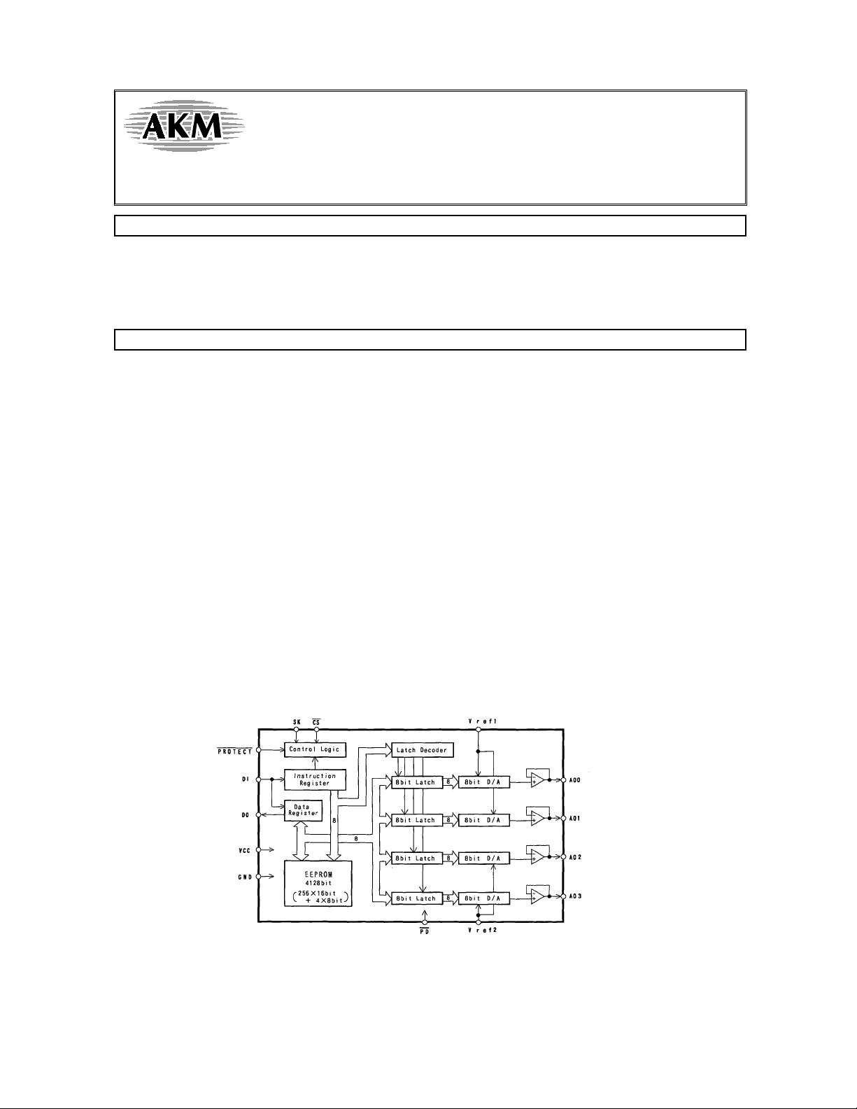
The AK9844 includes 4 channel, 8-bit D/A converters with on-chip output buffer amps and it is capable to
store the input digital data of each D/A converter by on-chip non-volatile CMOS EEPROM. The AK9844 is
optimally designed for various circuit adjustments for consumer and industrial equipments and it is ideally
suited for replacing mechanical trimmers.
FEATURES
EEPROM SECTION
•
4 word Õ 8-bit organization (Dedicated for DAC data)
•
256 word Õ 16-bit organization (General purpose memory)
•
Serial data interface
•
Sequential register read
•
Automatic write cycle
•
100K write cycles
•
10 year data retention
D/A SECTION
•
4 channels
•
Resolution : 8-bits
•
Differential Non-Linearity : 1.0 LSB
•
Linearity Error : 2.0 LSB
•
Output Voltage Range : GND ∼ VCC
AUTO READ Function
Power down mode
Block Diagram
DAD02E-00 1999/05
- 1 -
Page 2
ASAHI KASEI [AK9844]
Ordering Guide
AK9844F -20 to 70°C 14-pin SOP (1.27mm pitch)
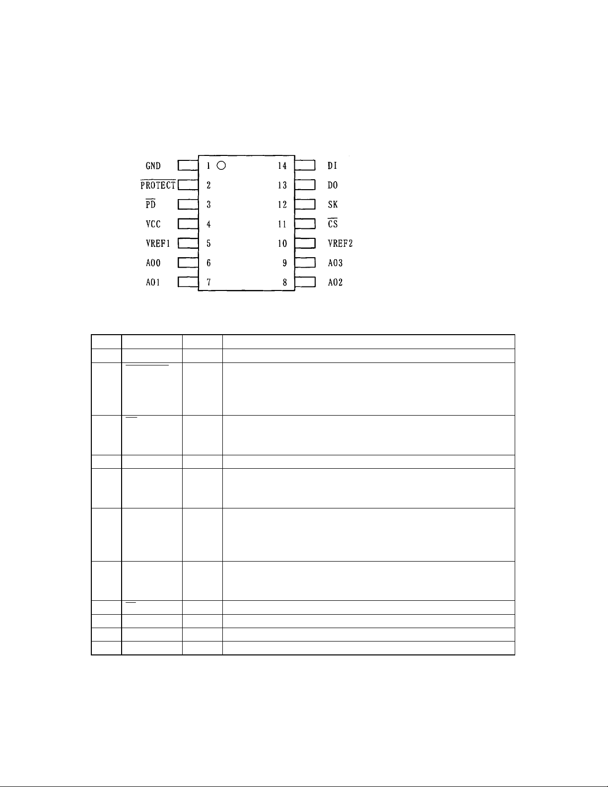
Pin Layout
Pin Description
No. Pin Name I/O Function
1 GND - Ground Pin, 0V
2 PROTECT I Protect Pin
"L" : Programming to the D/A Section of EEPROM is
disabled.
"H" : Normal operation
3 PD I Power-down Pin
"L" : Power down mode
"H" : Normal mode
4 VCC - Power Supply
5 VREF1 I Voltage Reference Input1
The analog output ranges of the AO0 and the AO1 are set
by the VREF1 pin.
6
AO0
7
AO1
8
AO2
O Analog Output Pins (8-bit D/A outputs)
AO3
10 VREF2 I Voltage Reference Input2
The analog output ranges of the AO2 and the AO3 are set
by the VREF2 pin.
11 CS I Chip Select Pin (Schmitt-trigger input)
12 SK I Serial Clock Pin (Schmitt-trigger input)
13 DO O Serial Data Input Pin
14 DI I Serial Data Output Pin
DAD02E-00 1999/05
- 2 -
Page 3

ASAHI KASEI [AK9844]
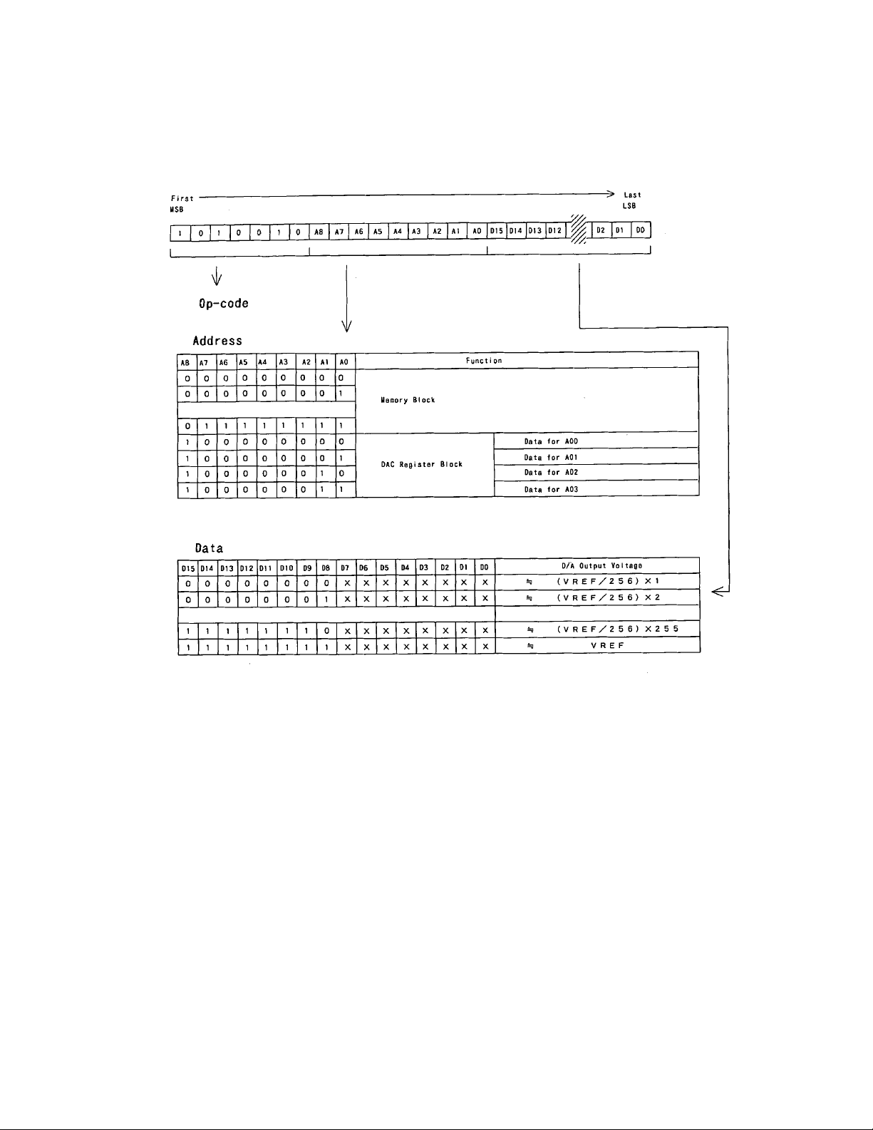
Functional Description
The AK9844 includes the EEPROM section and the D/A converter section which consists of 4 channel, 8bit
D/A converters with output buffer amps. The EEPROM section is divided into memory block and DAC register
block. The capacity of the memory block is 4096bits which are organized into 256 registers of 16bits each.
The DAC digital input data for D/A converters are stored in the DAC register block which is organized into 4
registers of 8bits each. The address for the memory block is "000000000" to "011111111". The address for
the DAC register is "100000000" to "100000011".
The configuration of the EEPROM section is showed on figure.1.
The AK9844 can connect to the serial communication port of popular one chip microcontrollers directly (3 line
negative clock synchronous interface). At write operation, the AK9844 takes in the write data from the DI pin
to a register synchronously with rising edge of the SK pin. At read operation, the AK9844 takes out the read
data from a register to the DO pin synchronously with falling edge of the SK pin.
The AK9844 has 6 instructions such as READ, WRITE, WREN, WRDS, PDEN and PDDS. The each
instruction is organized by op-code block(8bits), address block(8bits), and data(8bitsÕ2).The output of DAC is
set by storing the DAC digital input data in the DAC register block.
The DO pin is high impedance except that the DO pin outputs the read data and the status signal.
Figure.1 Configuration of the EEPROM section
DAD02E-00 1999/05
- 3 -
Page 4
ASAHI KASEI [AK9844]
Data Protection
To protect against accidental data disturb, the AK9844 has programming enable state and programming
disable state. In programming disable state, the programming operation is not executed.
When Vcc is applied to the AK9844, the AK9844 is powered up in the programming disable mode. The
programming instruction should be preceded by the WREN instruction. Once the WREN instruction is
executed, the programming state remains enabled until the WRDS ins tructio n is executed or VCC is removed
from the device. Execution of the READ instruction is independent of both WREN and WRDS instructions.
The AK9844 also can pro hibit to program into the DAC register block by the contr ol of the PROTECT pin.
When the PROTECT pin is "L", the programming into the DAC register block is not executed.
PROTECT pin PROTECT ="H" PROTECT ="L"
Programming State Enable Disable Enable Disable
Memory Block
DAC Register Block
{
:Programming into the block is executed.
Õ
:Programming into the block is not executed.
{
{
Õ
{
Õ
ÕÕÕ
Table.1 Relation between the programming operation and the PROTECT pin
DAD02E-00 1999/05
- 4 -
Page 5
ASAHI KASEI [AK9844]
Output of D/A converter
The AK9844 includes 4 channel, 8bit D/A converter. The output voltage ranges for AO0 and AO1 are set by
the VREF1 pin and the output voltage ranges for AO2 and AO3 are set by the VREF2 pin.
The output voltage can be set by the READ or WRITE instruction.
When the DAC register block is specified in the WRITE instruction, the output voltage for the specified D/A
converter is set. When the WRITE instruction is executed in case that the PROTECT pin is "H" and the
programming state is enabled, the output voltage for the specified D/A converter is set and the specified
address in the DAC register block in EEPROM is written with the data specified in the instruction.
When the WRITE instruction is executed in case that the PROTECT pin is "H" and the programming state is
disabled, the output voltage for the specified D/A converter is set and the specified address in the DAC
register block in EEPROM is not written with the data specified in the instruction. When the WRITE instruction
is executed in case that the PROTECT pin is "L", the output voltage for the specified D/A converter is not set
and the specified address in the DAC register block in EEPROM is not written with the data specified in the
instruction. The relation between the WRITE instruction and the DAC register block is showed on the table.2.
When the DAC register block is specified in the READ instruction, the output voltage for the specified D/A
converter is set by the data which is stored in the DAC register block in EEPROM, and the DO pin outputs the
data in the specified address.
Execution of the READ instruction is independent of the PROTECT pin and the programming state.
PROTECT
pin
"H"
Programming
State
DAC register block
(EEPROM Section)
Enable The specified address in the
DAC register block is written
with the data specified in
the instruction.
Disable
Enable "L"
The data in the DAC register
section does not change.
Disable
Output of DAC
(D/A Converter Section)
The output voltage for the
specified D/A converter is
set by the data specified
in the instruction.
The output of the DAC
does not change.
Table.2 Relation between the WRITE instruction and the DAC register block
{{{{
AUTO READ Function
When Vcc is applied to the AK9844, the data on EEPROM are read out and loaded at a time to each
corresponding D/A (4 channels total) automatically, starting from AO0 to AO3 in ascending order. Then each
D/A analog output is settled to pre-determined value.
If the CS pin goes to "H" and then goes to "L" after "power-up" with the PROTECT pin and the CS pin left "L",
AUTO READ cycle is initiated. After the CS pin goes to "L", 4 channel D/A outputs are settled to predetermined value within 2ms.
In AUTO READ cycle, the SK pin and the DI pin become "don't care" and the serial data do not output.
If the WREN instruction is executed after AUTO READ cycle is completed, programming into the memory
block on the internal EEPROM is enabled.
DAD02E-00 1999/05
- 5 -
Page 6
ASAHI KASEI [AK9844]
Instruction and Data Format
The instructions consist of op-code(8bits), address(8bits) and data(8bitsÕ2). The followings are the instruction
and data set at WRITE execution.
DAD02E-00 1999/05
- 6 -
Page 7

ASAHI KASEI [AK9844]
Power Down Function
There are the power down mode and the normal mode in AK9844. When the AK9844 is in power down mode,
the outputs of D/A are "High impedance" and the DAC section is in the standby mode and the power
consumption of the AK9844 is decreased.
The power down mode of AK9844 can be determined by the control of the PD pin or the PDEN/ PDDS
instructions.
When the PD pin is low level, the AK9844 is in power down mode. When the PD pin is high level, the state of
the AK9844 can be determined by PDEN/PDDS instructions. When the PD pin is High level and the PDEN
instruction is executed, the AK9844 becomes the power down mode. Once the AK9844 becomes the power
down mode, the AK9844 is in the power down mode until the PDDS instruction is executed. When the PDDS
instruction is executed, the AK9844 becomes the normal mode.
If the CS pin is High level in the power down mode, the EEPROM section also becomes the standby mode
and the AK9844 becomes the lower power-down mode.
The relation between the PD pin and the PDEN/PDDS instructions is showed on table.3. The relation between
the power down mode and the DAC/EEPROM section is showed on table.4. The state at the time AK9844 is
powered up is showed on table.5.
PD pin instruction mode
PDEN Low level
power down mode
PDDS
PDEN power down mode High level
PDDS normal mode
Table.3 Relation between the PD pin and the PDEN/PDDS instructions
State DAC section EEPROM section
normal mode normal mode normal mode
power down mode1 CSpin=L standby mode normal mode
power down mode2 CSpin=H standby mode standby mode
Table.4 Relation between the power down mode and the DAC/EEPROM section
Condition at the time AK9844 is powered on State
CSpin=L power down mode1 PDpin = "L"
CSpin=H power down mode2
PDpin = "H" normal mode
Table.5 State at the time AK9844 is powered up
Precautions for use
1) Output voltage of D/A converter at the time the AK9844 is powered up
At the time the AK9844 is powered up, the D/A converters output "Vref/2" until the instruction or AUTO
READ is executed.
2) Power Supply Decoup li ng
On the boards, decoupling capacitors(0.1uF) between power supply pins(VCC,VREF1,VREF2) and GND
should be located as near as possible to the part.
DAD02E-00 1999/05
- 7 -
Page 8

ASAHI KASEI [AK9844]
Instruction Set
The AK9844 has 6 instructions such as READ, WRITE, WREN, WRDS, PDEN, PDDS. Each instruction
consists of Op-code, address and data. The instruction set is showed on table.6.
When the instructi ons are executed consecutively, the CS pin should be brought to high level for a mini mum of
1us(tCS) between consecutive instruction cycle.
Instruction Op-code Address Data Comments
READ
WRITE
WREN
WRDS
PDEN
PDDS
1 0 1 0 1 0 0
1 0 1 0 0 1 0
1 0 1 0 0 0 1
1 0 1 0 0 0 0
1 0 1 0 1 1 0
1 0 1 0 0 1 1
A7 A6 A5 A4 A3 A2 A1 A0
A8
A7 A6 A5 A4 A3 A2 A1 A0
A8
∗ ∗ ∗ ∗ ∗ ∗
∗
1
∗ ∗ ∗ ∗ ∗ ∗
∗
0
∗ ∗ ∗ ∗ ∗ ∗
∗
0
∗ ∗ ∗ ∗ ∗ ∗
∗
0
D15∼D0
D15∼D0
∗
∗
∗
∗
Read register
Write register
∗∼
Write enable
∗∼
Write Disable
∗∼
Power down enable
∗∼
Power down desable
∗: Don't Care
Table.6 Instruction set
WRITE
The WRITE instruction is followed by 16 bits of data to be written into the specified address. After the 32nd
rising edge of SK to read DO in, the AK9844 will be put into the automatic write time-out period. During the
automatic write time-out period (Busy status), the CS pin need not be high level.
The DO pin indicates the Ready/Busy status of the EEPROM in AK9844. After the 32nd rising edge of SK to
read DO in, the AK9844 will be put into the automatic write time-out period.
When the automatic write time-out period start, the DO pin outputs the Ready/Busy status.
When the DO pin outputs low level, the AK9844 is in the automatic write time-out and the next instruction can
not be accepted. When the DO pin outputs high level, the automatic write time-out period has ended and the
AK9844 is ready for a next instruction.
When the CS pin is changed to high level after confirmation of Ready/Busy signal on the DO pin, the DO pin
becomes "Hi-Z". The Ready/Busy signal can be confirmed until the initial 1 bit of the next instruction inputs
from the execution of the WRITE instruction.
WRITE instruction
DAD02E-00 1999/05
- 8 -
Page 9

ASAHI KASEI [AK9844]
READ
The read instruction is the only instruction which outputs serial data on the DO pin.
After a read instruction is received, the instruction and address are decoded, followed by data transfer from
the memory register into a 16 bit serial-out shift register. When the 17th falling edge of SK is received, the Do
pin will come out of high impedance state and shift out the data from D15 first in descending order which is
located at the address specified in the instruction.
{
Sequential register read
The data in the next address can be read sequentially to provide clock. The memory automatically cycles
to the next register after each 16 data bits are clocked out.
The sequential register read function is effective for address:A7∼A0. When the highest address is
reached($0FF/$103), the address counter rolls over to address $000/$100 allowing the read cycle to be
continued indefinitely.
READ instruction
WREN/WRDS
When Vcc is applied to the part, it powers up in the programming disable(WRDS) state.
Programming must be preceded by a programming enable(WREN) instruction. Programming remains enabled
until a programming disable(WRDS) instruction is executed or Vcc is removed from the part. The
programming disable instruction is provided to protect against accidental data disturb. Execution of a read
instruction is not affected by both WREN and WRDS instruction.
WREN/WRDS instruction
DAD02E-00 1999/05
- 9 -
Page 10

ASAHI KASEI [AK9844]
PDEN/PDDS
The AK9844 has the power-down mode an d the nor m al mode. When the PDEN ins tr uction is executed while
the PD pin is high level, the AK9844 bec om es the power-down mode. The AK9844 is in the power-down mode
until PDDS instruction is executed. After the PD DS instruction is executed, the AK9844 chang ed to normal
mode from power-down mode.
In case that the PD pin is low level, the PDEN/PDDS instructions are invalid and are not executed.
PDDS instruction
DAD02E-00 1999/05
- 10 -
Page 11

ASAHI KASEI [AK9844]
ABSOLUTE MAXIMUM RATINGS
Parameter Symbol Condition Spec. Unit
DC Pow er Supplies
Input Voltage
Ambient Temperature
VCC
VIO
Ta
relative to GND
relative to GND
-0.3∼+6.5
-0.3∼VCC+0.3
-20∼+70
V
V
C
°
(power applied)
Storage Temperature
TST
-65∼+150
C
°
RECOMMENDED OPERATING CONDITIONS
Parameter Symbol Condition min typ max Unit
VCC1 DAC operation 4.5 5.5 V Power supplies
VCC2 EEPROM operation 2.2 5.5 V
Analog Output Load
AOC 100 pF
Load Capacitance
DAD02E-00 1999/05
- 11 -
Page 12

ASAHI KASEI [AK9844]
ELECTRICAL CHARACTERISTICS
DC Characteristics
(VCC=+2.2V∼5.5V, GND=0V, Ta=-20∼70°C unless otherwise specified)
Parameter Symbol Condition min typ max Unit
Power Consumption
IDD1 Normal mode
8.0 10.0 mA
WRITE,1/tSKP=1MHz
IDD2 Normal mode
3.0 6.0 mA
READ,1/tSKP=1MHz
IDD3 Power down mode1
1.0 mA
READ,1/tSKP=1MHz
IDD4 Power down mode2 10.0 uA
Note1.,Note2.,Note3.
Input High Voltage
CS,SK,PROTECTpin
PD,DIpin
Input Low Voltage
CS,SK,PROTECTpin
PD,DIpin
VIH
VIL
80%VCC
70%VCC
20%VCC
30%VCC
V
V
V
V
Output High Voltage VOH IOH=-50uA VCC-0.3 V
Output Low Voltage VOL IOL=1.0mA 0.4 V
Input Leakage Current ILI VIN=VCC 10.0 uA
3 State Leakage
IOZ CS="H"
10.0 uA
Current
Note1. All input pins are connected to either Vcc or GND.
Note2. DO=OPEN
Note3. Please refer to "Power Down Function" regarding power down mode.
DAD02E-00 1999/05
- 12 -
Page 13

ASAHI KASEI [AK9844]
AC Characteristics
1)EEPROM section
(VCC=+2.2V∼5.5V, GND=0V, Ta=-20∼70°C unless otherwise specified)
Parameter Symbol Condition min typ max Unit
SK cycle1 tSKP1 (Note4) 1.0 us
SK pulse width1 "L"
"H"
tSWL1
tSWH1 (Note4)
400
400
ns
ns
SK cycle2 tSKP2 (Note5) 4.0 us
SK pulse width2 "L"
"H"
tSWL2
tSWH2 (Note5)
1
1
us
us
CS Setup Time tCSS 100 ns
CS Hold Time tCSH (Note6) 100 ns
SK Setup time tSKS 100 ns
Data Setup Time tDIS 200 ns
Data Hold Time tDIH 200 ns
Data Output Delay tPD CL=100pF 300 ns
Selftimed Program Time tE/W 15 ms
Write Recovery Time tRC 100 ns
Min CS High Time tCS 1.0 us
Do High-Z Time tOZ 500 ns
Note4. 4.5V≤VCC≤5.5V
Note5. 2.2V≤VCC<4.5V
Note6. In case that the data of the DAC section is not changed and the output of the DAC is changed,
tCSH is min.1us.
DAD02E-00 1999/05
- 13 -
Page 14

ASAHI KASEI [AK9844]
2) DAC section
(VCC=+5V10%, GND=0V, Ta=-20∼70°C unless otherwise specified)
Parameter Symbol Condition min typ max Unit
D/A Reference Voltage
A0,A1
A2,A3
VREF1
VREF2
3.5
3.5
VCC
VCC
V
V
D/A Reference current
IREF VREF=5.0V 200 uA
Resolution Monotonicity 8 bit
Differential Non-Lineality DNL -1 0 +1 LSB
Integral Non-Lineality
NL -2.0 0 +2.0 LSB
VCC=VREF=5.0V
1LSB=VREF/256
(Note8)
Error or
EZERO + 0.1 V
IAO=0.0uA
Input data "00" (Note7)
Error for
EFULL
C
+0.1 V
L
=100pF
Input data "FF" (Note7)
Buffer-AMP Output
VAO
| IAO |≤200uA
0.2 VCC-0.2 V
Voltage Range
Buffer-AMP Output
VAO
| IAO |≤500uA
0.3 VCC-0.3 V
Voltage Range
Setup Time in AUTO READ tARS 500 us
D/A Settling Time tLDD CL=100pF 100 us
Note7. Please refer to the figure.2.
Note8. Integral Non-Linearity is the error between the actual line and the ideal line. The ideal line exhibits a
perfect linear DAC output characterist ics between the input digit al data "0 0" and the input di git al
data "FF".
5 Please refer to "Instruction and Data Format" regarding the relation between input digital data and DAC
output voltage.
Figure.2 DAC output characteristics(IAO=0.0uA)
DAD02E-00 1999/05
- 14 -
Page 15

ASAHI KASEI [AK9844]
Timing waveform
Waveform in READ instruction
DAD02E-00 1999/05
- 15 -
Page 16

ASAHI KASEI [AK9844]
(Note) In case that the data of the DAC section is not changed and the output of the DAC is changed,
Ready/Busy signal does not output on DO pin.
Waveform in AUTO READ
DAD02E-00 1999/05
- 16 -
Page 17

IMPORTANT NOTICE
z These products and their specifications are subject to change without notice. Before
considering any use or application, consult the Asahi Kasei Microsystems Co., Ltd. (AKM)
sales office or authorized distributor concerning their current status.
z AKM assumes no liability for infringement of any patent, intellectual property, or other
right in the application or use of any information contained herein.
z Any export of these products, or devices or systems containing them, may require an
export license or other official approval under the law and regulations o f the country of
export pertaining to customs and tariffs, currency exchange, or strategic materials.
z AKM products are neither intended nor author ized for use as critical compo nents in any
safety, life support, or other hazard related device or system, and AKM assumes no
responsibility relating to any such use, except with the express written consent of the
Representative Director of AKM. As used here:
(a) A hazard related device or system is one designed or intended for life support or
maintenance of safety or for applications in medicine, aerospace, nuclear ener gy, or
other fields, in which its failure to function or perf orm may reasonably be expected to
result in loss of life or in significant injury or damage to person or property.
(b) A critical component is one whose failure to func tion or perform may reasonably be
expected to result, whether directly or indirectly, in the loss of the safety or
effectiveness of the device or system containing it, and which must therefore meet
very high standards of performance and reliability.
z It is the responsibility of the buyer or distributor of an AKM product who distributes,
disposes of, or otherwise places the product with a third party to notify that party in
advance of the above content and conditions, and the buyer or distributor agrees to
assume any and all re sponsibility and liability for and ho ld AKM harmless fr om any and
all claims arising from the use of said product in the absence of such notification.
 Loading...