

Page 1
ASAHI KASEI [AK9822/24]
AK9822 / 24
2K / 4Kbit EEPROM with 2ch 8bit D/A Converter
General Description
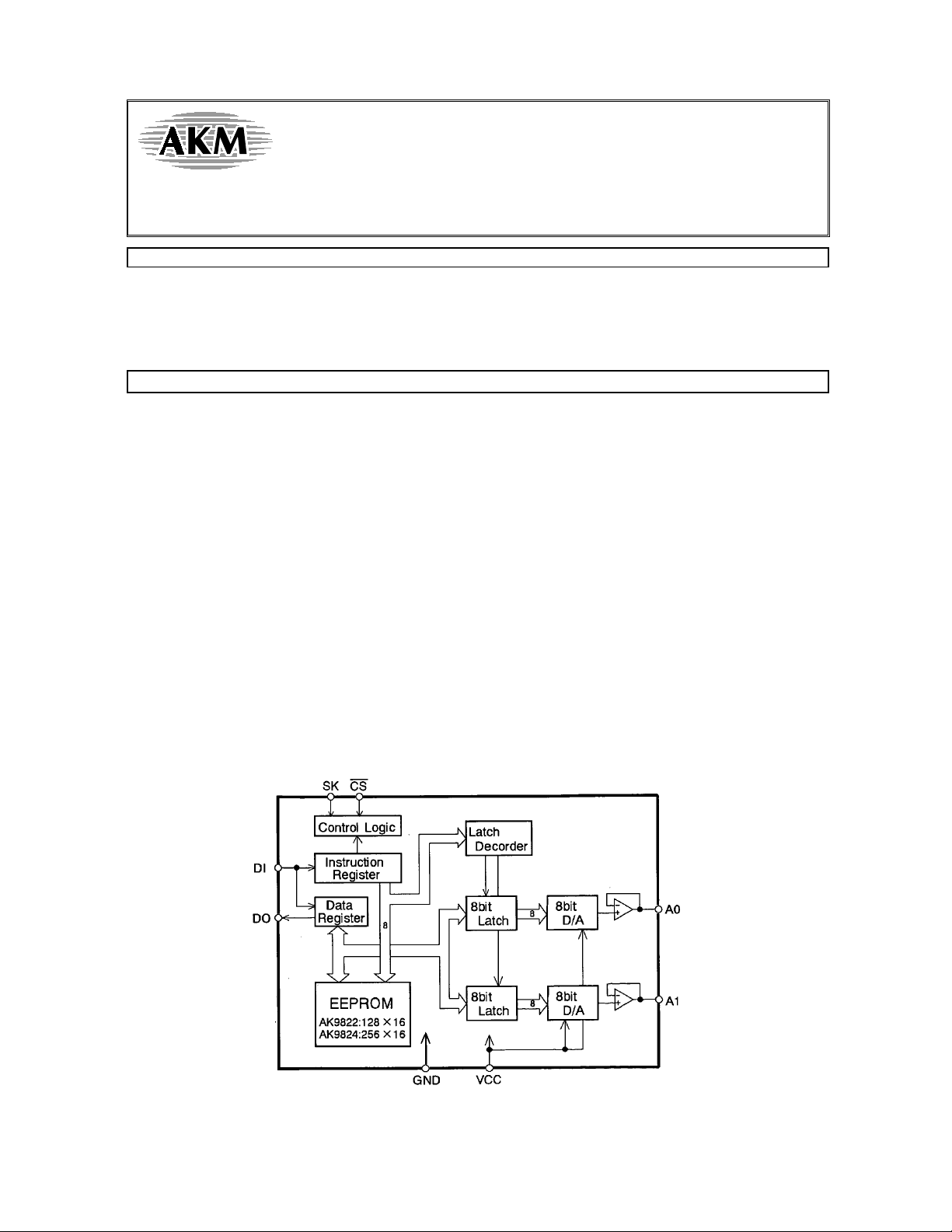
The AK9822/24 includes 2 channel, 8 bit D/A convert ers wit h on-chip output buffer amps and it is
capable to store the input digital data of each D/A converter by on-chip non-volatile CMOS
EEPROM. The AK9822/24 is optimally designed for various circuit adjustments for consumer and
industrial equipments and it is ideally suited for replacing mechanical trimmers.
Feature
EEPROM section
• • •
AK9822
AK9824
One chip microcomputer interface
Sequential register read
128 words Õ 16bit
• • •
256 words Õ 16bit
D/A Converter section
2 channel
Resolution : 8bit
Differential Non-Linearity : 1.0 LSB
Linearity Error : 1.5 LSB
Output Voltage Range : GND ∼ VCC
Wide VCC operation
•
EEPROM section : 1.8V∼5.5V
•
D/A Converter Section : 2.7V∼5.5V
Power Down Function
Block Diagram
DAD01E-00 1999/05
- 1 -
Page 2
ASAHI KASEI [AK9822/24]
Ordering Guide
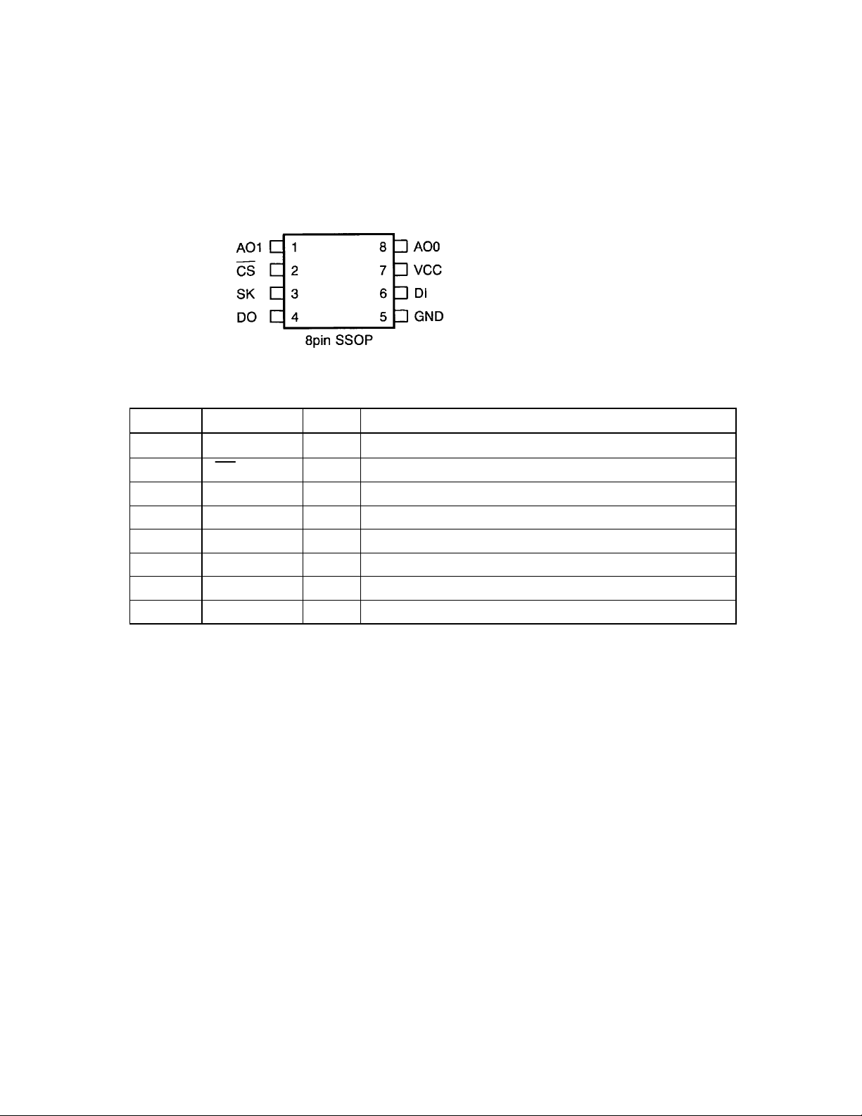
Pin Layout
Pin Description
AK9822M -40°C∼+85°C 8pin SSOP
AK9824M -40°C∼+85°C 8pin SSOP
No. Pin Name I/O Function
1 AO1 O Analog Output Pin
2 CS I Chip Select Pin (Schmitt-trigger input)
3 SK I Serial Clock Pin (Schmitt-tr igger input)
4 DO O Serial Data Output Pin
5 GND - Ground Pin
6 DI I Serial Data Input Pin
7 VCC - Power Supply
8 AO0 O Analog Output Pin
DAD01E-00 1999/05
- 2 -
Page 3
ASAHI KASEI [AK9822/24]
Functional Description
The AK9822/24 is composed of EEPROM and the 8bit D/A converter of two channels with the
output buffer amplifier.
The AK9822/24 can connect to the serial communication port of popular one chip microcomputer
directly (3 line negative clock synchronous interface).
The AK9822/24 takes the data of the DI pin by the rising edge of the SK pin and outputs the data
from the DO pin by the falling edge of the SK pin.
The AK9822/24 has 7 instructions such as READ, WRITE, WREN, WRDS, PDEN, PDDS and CALL.
The AK9822/24 is operated by inputting these instructions from the serial interface. Each instruction
is organized by op-code block (8bits), address block (8bits) and data (8bitsÕ2).
The DO pin is "Hi-Z" state except that the DO pin outputs the data of the internal register and the
status of Ready/Busy.
WRITE protection function
There are two states such as the WRITE enable state and the WRITE disable state in the
AK9822/24. In the WRITE disable state the WRITE instruction becomes invalid and is not executed.
When Vcc is applied to the part, the part powers up in the WRITE disable state and the part
becomes the WRITE enable state by inputting the WREN instruction. The WRITE enable state
continues until the WRDS instruction is executed or Vcc is removed from the part.
Execution of a READ instruction is independent of both WREN and WRDS instructions.
Power down function
There are two modes such as the power down mode and the normal mode in the AK9822/24. When
the AK9822/24 is in the power down mode, the D/A converter section is in the standby state. At this
time, the outputs of the D/A converters become "Hi-Z".
When Vcc is applied to the part, the AK9822/24 is in the power down mode. When a AUTO READ
function is executed, the part becomes the nor mal mode. After the AUTO READ function is
executed, the mode of the part can be switched by the PDEN and PDDS instructions. The
AK9822/24 becomes the power down mode by inputting the PDEN instruction. The part is in the
power down mode until the PDDS instruction is executed. When the PDDS instruction is executed,
the part becomes the normal mode.
When returning to the normal mode from the power down mode, the D/A converters output the
voltage value set before entering the power down mode. The relation between the D/A converter
state and the mode are shown in the table 1.
Mode State of D/A converter
Power down mode standby
Normal mode normal
Table 1. The relation between the state of D/A converter and the mode
DAD01E-00 1999/05
- 3 -
Page 4
ASAHI KASEI [AK9822/24]
Output of D/A converter
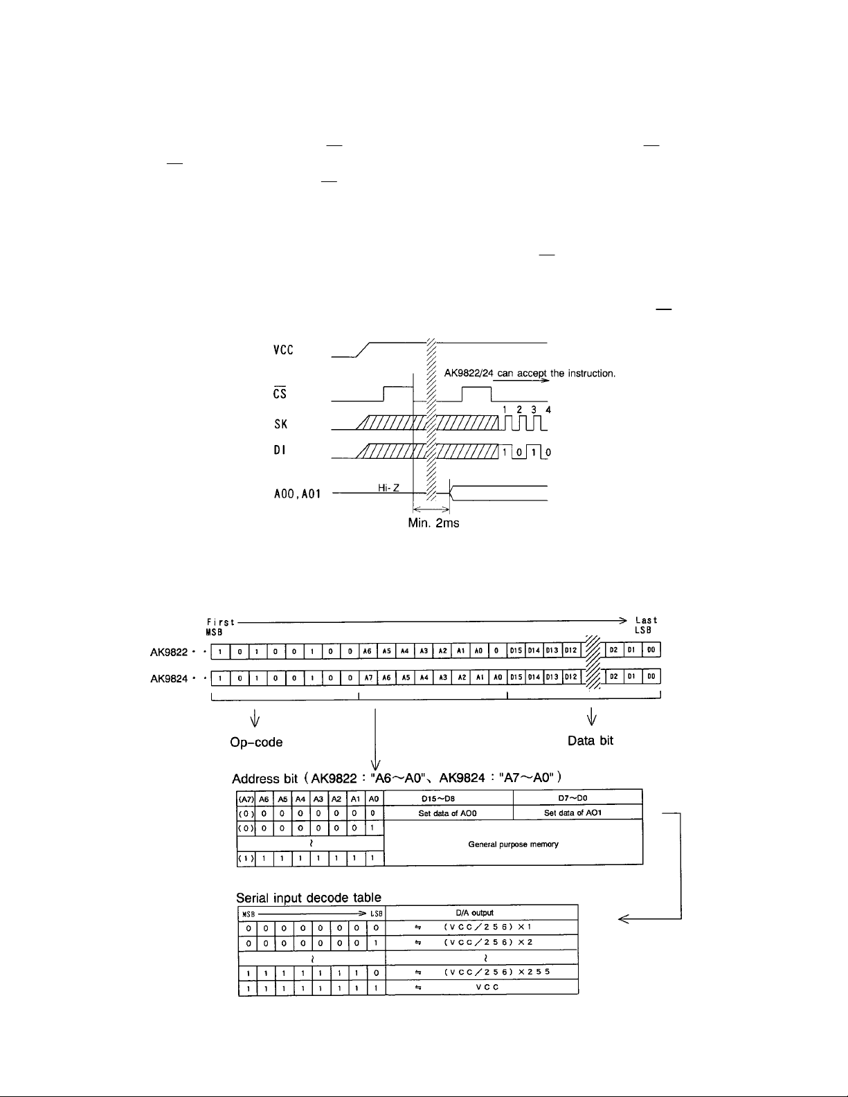
The output of the D/A converters can be set by the WRITE and the CALL instructions.
Upper 8bit data (D15∼D8) of the first address of the internal EEPROM (the address "0")
corresponds to "AO" of the D/A converter output. Lower 8bit data (D7∼D0) of the address "0"
corresponds to "A1". The internal composition of EEPROM is shown in the table2.
Address
D15∼D8 D7∼D0
0 Set data of A0 Set data of A1
1 General purpose memory
127(AK9822)
General purpose memory
/255(AK9824)
Table2. Internal composition of EEPROM
If the WRITE instruction by which the address "0" is specified is executed at the normal mode, the
outputs of the D/A converter of A0 and A1 are set by the specified data.
When the WRITE instruction by which the address "0" is specified is executed at the WRITE enable
state and the normal mode, the data is written in the address "0" of EEPROM and the outputs of the
D/A converter are set. When the WRITE instr uction by which the address "0" is specified is
executed at the WRITE disable state and the normal mode, the data is not written in EEPROM and
the outputs of the D/A converter are set. Table3 shows the relation between EEPROM, D/A
converter and WRITE instruction.
State of AK9822/24 State of address"0" Output of A0 and A1
mode
WRITE enable The data change to the specified data.Power down
WRITE disable The data does not change.
WRITE enable The data change to the specified data.Normal mode
WRITE disable
The data does not change.
The DAC outputs
are "Hi-Z".
The DAC outputs
change to the
specified data.
Table3. Relation between EEPROM, D/A converter and WRITE instruction
If the CALL instruction is executed, the outputs of the D/A converter are set by the data of the
general purpose memory (AK9822:address "1" -"127", AK9824:address "1" -"255"). The CALL
instruction is composed by the op-code and the address.
When the CALL instruction is executed at the normal mode, the D/A converter output of A0 is set by
the upper 8bit data (D15∼D8) of the specified address and the output of A1 is set by the lower 8bit
data (D7∼D0). The CALL instruction is not executed at the power down mode.
DAD01E-00 1999/05
- 4 -
Page 5
ASAHI KASEI [AK9822/24]
AUTO READ function
AUTO READ function automatically reads the content of EEPROM and sets the output of the D/A
converter of two channels, when Vcc is applied to the part.
When Vcc is applied to the part in CS="L", the AUTO READ function starts by falling CS pin first.
After the CS pin is made a low level, the output of AO0 and AO1 is set within 2ms. At this time, the
input pins (SK, DI) other than the CS pin are not accepted, and the serial data is not output from the
DO pin. If the WREN instruction is executed after the AUTO READ function finished, AK9822/24
becomes the WRITE enable state.
After Vcc is applied to the part, the AUTO READ function is executed only once.
AUTO READ function is executed when Vcc is applied to the part in CS="L".
(note) Because AK9822/24 always executes the AUTO READ function first after Vcc is applied to
the part, AK9822/24 is not able to accept the instruction for the first period of "L" of the CS.
Instruction and Composition of the data
Each instruction consist of op-code, address, and data (8bitÕ2) composed in each 8bit. The
composition of the WRITE instruction is shown as follows.
DAD01E-00 1999/05
- 5 -
Page 6
ASAHI KASEI [AK9822/24]
Instruction Set
The AK9822/24 has 7 instructions such as READ, WRITE, WREN, WRDS, PDEN, PDDS, CALL.
Each instruction consists of Op-code, address and data. The instruction set is shown in the table4
and table5.
When the instructions are executed consecutively, the CS pin should be brought to a high level for a
minimum of tCS between consecutive instruction cycle.
Instruction Op-code Address Data Comments
READ
WRITE
WREN
WRDS
PDEN
PDDS
CALL
TEST
1 0 1 0 1 0 0 0
1 0 1 0 0 1 0 0
1 0 1 0 0 0 1 1
1 0 1 0 0 0 0 0
1 0 1 0 1 1 0 0
1 0 1 0 0 1 1 0
1 0 1 0 0 0 1 0
1 0 1 0 1 1 1 1
A6 A5 A4 A3 A2 A1 A0 0
A6 A5 A4 A3 A2 A1 A0 0
********
********
********
********
A6 A5 A4 A3 A2 A1 A0 0
********
D15∼D0
D15∼D0
∼
*
∼
*
∼
*
∼
*
∼
*
∼
*
read memory
write memory
write enable
write disable
power down enable
power down disable
set DAC outputs
TEST (note)
(note) User can't use this instruction. *: Don't Care
Table4. Instruction set for AK9822
Instruction Op-code Address Data Comments
READ
WRITE
WREN
WRDS
PDEN
PDDS
CALL
TEST
1 0 1 0 1 0 0 0
1 0 1 0 0 1 0 0
1 0 1 0 0 0 1 1
1 0 1 0 0 0 0 0
1 0 1 0 1 1 0 0
1 0 1 0 0 1 1 0
1 0 1 0 0 0 1 0
1 0 1 0 1 1 1 1
A7 A6 A5 A4 A3 A2 A1 A0
A7 A6 A5 A4 A3 A2 A1 A0
********
********
********
********
A7 A6 A5 A4 A3 A2 A1 A0
********
D15∼D0
D15∼D0
∼
*
∼
*
∼
*
∼
*
∼
*
∼
*
read memory
write memory
write enable
write disable
power down enable
power down disable
set DAC outputs
TEST (note)
(note) User can't use this instruction. *: Don't Care
Table5. Instruction set for AK9824
DAD01E-00 1999/05
- 6 -
Page 7

ASAHI KASEI [AK9822/24]
WRITE
The WRITE instruction is followed by 16 bits of data to be written into the specified address. After
the 32nd rising edge of SK to read the DI pin in, the AK9822/24 will be put into the automatic write
time-out period.
The DO pin indicates the Ready/Busy status of the EEPROM in the AK9822/24. After the 32nd
rising edge of SK to read the Di pin in, the AK9822/24 will be put into the automatic write time-out
period. When the automatic write time-out period starts, the DO pin outputs the Ready/Busy status.
When the DO pin outputs the low level, the AK9822/24 is in the automatic write time-out and the
next instruction can not be accepted. When the DO pin outputs the high level, the automatic write
time-out period has ended and the AK9822/24 is ready for a next instruction.
When the CS pin is changed to high level after confirmation of Ready/Busy signal on the DO pin, the
DO pin becomes "Hi-Z". The Ready/Busy signal outputs until the CS pin is changed to high level, or
the initial 1 bit ("1") of the next instruction is given to the part.
WRITE (AK9824)
DAD01E-00 1999/05
- 7 -
Page 8

ASAHI KASEI [AK9822/24]
READ
The READ instruction is the only instruction which outputs serial data on the DO pin. When the 17th
falling edge of SK is received, the Do pin will come out of high impedance state and shift out the
data from D15 first in descending order which is located at the address specified in the instruction.
Sequential READ
{
When the clock is provided on the SK pin after the data in the specified address is read, the data
in the next address is read.
• •
AK9822
When the clock is provided on the SK pin after the data in the address:7F (Hex) is
read, the data in the address:00 (Hex) is read.
• •
AK9824
When the clock is provided on the SK pin after the data in the address:FF (Hex) is
read, the data in the address:00 (Hex) is read.
READ (AK9824)
DAD01E-00 1999/05
- 8 -
Page 9

ASAHI KASEI [AK9822/24]
WREN/WRDS
There are two states such as the WRITE enable state and the WRITE disable state in the
AK9822/24. In the WRITE disable state the WRITE instruction becomes invalid and is not executed.
When Vcc is applied to the part, it powers up in the WRITE disable stat e. The WRITE instruction
must be preceded by a WREN instruction. This state remains enabled until a WRDS instruction is
executed or Vcc is removed from the part.
Execution of a read instruction is not affected by both WREN and WRDS instruction.
WREN/WRDS (AK9822/24)
PDEN/PDDS
There are two modes such as the power down mode and the normal mode in the AK9822/24. The
mode of the part can be switched by the PDEN and PDDS instructions. The AK9822/24 becomes
the power down mode by inputting the PDEN instructions. When the PDDS instruction is executed,
the part becomes the normal mode.
When returning to the normal mode from the power down mode, the D/A converters output the
voltage value set before entering the power down mode.
PDDS (AK9822/24)
DAD01E-00 1999/05
- 9 -
Page 10

ASAHI KASEI [AK9822/24]
CALL
The outputs of the D/A converters is set by inputting a CALL instruction. Upper 8bit data (D15aD8)
of the specified address corresponds to "A0". Lower 8bit data (D7aD0) of the specified address
corresponds to "A1".
The CALL instruction is not executed at the power down mode.
CALL (AK9824)
DAD01E-00 1999/05
- 10 -
Page 11

ASAHI KASEI [AK9822/24]
Absolute Maximum Ratings
Parameter Symbol Conditions Spec. Units
Power supply
Input voltage
Ambient temperature
Storage temperature
VCC
VIO
Relative to GND
Relative to GND
Ta
TST
Recommended Operating conditions
-0.6∼+7.0
-0.6∼VCC+0.6
-40∼+85
-65∼+150
V
V
°
C
°
C
Parameter Symbol Conditions min typ max Units
VCC1 DAC operation 2.7 5.5 V Power supply
VCC2 EEPROM operation 1.8 5.5 V
Analog output
IAL1 1 mA
source current1
Analog output
IAH1
3.6V≤VCC ≤5.5V
1mA
sink current1
Analog output
IAL2 500 uA
source current2
Analog output
IAH2
2.7V≤VCC<3.6V
500 uA
sink current2
Analog output
AOC 1.0 uF
load capacitance
DAD01E-00 1999/05
- 11 -
Page 12

ASAHI KASEI [AK9822/24]
Electrical characteristics
DC characteristi cs
(VCC=+1.8V∼5.5V, GND=0V, Ta=-40∼+85°C unless otherwise specified )
Parameter
Operating
Symbol
IDD1 Normal mode
power consumption
IDD2 Normal mode
IDD3 Power down mode
(note1),(note3)
Standby (note2),(note3)
IDD4 Power down mode
power consumption
Input high voltage
CS,SK pin
Input high voltage
DI pin
Input low voltage
CS,SK pin
Input low voltage
DI pin
VIH1
VIH2
VIH3
VIH4
VIL1
VIL2
VIL3
VIL4
Output high voltage VOH1
Conditions min max Units
WRITE, 1/tSKP=2MHz
READ, 1/tSKP=2MHz
READ, 1/tSKP=2MHz
standby(CS="H")
2.5V≤VCC≤5.5V
1.8V≤VCC<2.5V
2.5V≤VCC≤5.5V
1.8V≤VCC<2.5V
2.5V≤VCC≤5.5V
1.8V≤VCC<2.5V
(note4),IOH=-50uA
0.8ÕVCC
0.9ÕVCC
0.7ÕVCC
0.8ÕVCC
VCC-0.3
5.5 mA
2.3 mA
0.75 mA
1.0 uA
0.2ÕVCC
0.1ÕVCC
0.3ÕVCC
0.2ÕVCC
V
V
V
V
V
V
V
VOH2
Output low voltage VO L1
VOL2
Input leakage current ILI VCC=5.5V,VIN=VCC
3 state
leakage current
(note5),IOH=-50uA
(note4),IOL=1.0mA
(note5),IOL=0.1mA
IOZ VCC=5.5V,DO=VCC
CS="H"
VCC-0.3
0.4
0.4
1.0
1.0
note1. VCC=5.5V,VIN=VIH/VIL,DO=open
note2. VCC=5.5V,SK/DI=VCC/GND,DO=open
note3. Please refer to the "Power down function" regarding the power down mode.
note4. 2.5V≤VCC≤5.5V
note5. 1.8V≤VCC<2.5V
V
V
V
uA
uA
DAD01E-00 1999/05
- 12 -
Page 13

ASAHI KASEI [AK9822/24]
AC characteristics
1)EEPROM section
(VCC=+1.8V∼5.5V, GND=0V, Ta=-40∼+85°C unless otherwise specified )
Parameter
SK cycle tSKP1
SK pulse width tSKW1
SK pulse high level width
(note10)
Symbol
tSKP2
tSKW2
tSKH1
tSKH2
tSKH3
Conditions min max Units
(note6),(note7)
(note8)
(note6),(note7)
(note8)
(note6)
(note7)
(note8)
500
1.5
250
750
250
500
750
ns
us
ns
ns
ns
ns
ns
CS setup time tCSS 100 ns
CS hold time
tCSH1 READ
100 ns
WREN, WRDS
PDEN, PDDS
tCSH2 CALL
2us
WRITE (note9)
SK setup time tSKS 100 ns
Data setup time tDIS1
tDIS2
tDIS3
data hold time tDIH1
tDIH2
tDIH3
(note6)
(note7)
(note8)
(note6)
(note7)
(note8)
100
150
200
100
150
200
ns
ns
ns
ns
ns
ns
DO pin output delay
(note11), (note13)
tPD1
tPD2
tPD3
(note6)
(note7)
(note8)
150
250
500
ns
ns
ns
Selftimed program time tE/W 10 ms
Write recovery time tRC 100 ns
Min. CS high time (note12) tCS 250 ns
DO pin high-Z time tOZ 500 ns
note6. 4.0V≤VCC≤5.5V
note7. 2.5V≤VCC<4.0V
note8. 1.8V≤VCC<2.5V
note9. In case of the following case, tCSH is min.100ns.
•
The WRITE instruction by which the address "0" is specified is executed at the WRITE
enable state.
•
The WRITE instruction by which the address "1∼127/255" is specified is executed.
note10. The tSKH is the high pulse width of 16th SK pulse in READ operation. When the
data in the next address are read sequentially by continuing to provide clock, tSKH are
applied to the high pulse width of 32nd and 48th (multiple of 16) SK pulse in READ
operation.
note11. In case that Ready/Busy signal output, tPD is min.1us.
note12. The first CS high time is the tACS after Vcc is applied to the part.
note13. CL=100pF
DAD01E-00 1999/05
- 13 -
Page 14

ASAHI KASEI [AK9822/24]
2)D/A converter section
(2.7V≤VCC≤5.5V, GND=0V, Ta=-40∼+85°C unless otherwise specified)
Parameter
Symbol
Conditions min typ max Units
Resolution Monotonic 8 bit
Differential
non-linearity
linearity error (note14) NL
DNL -1.0 0 +1.0 LSB
AO=OPEN
≤
0.1
AO
≤
VCC-0.1
-1.5 0 +1.5 LSB
VAO1 |IAO|= 0uA 0.1 VCC-0.1 V Buffer amp
output voltage range
3.6V≤VCC≤5.5V
VAO2
|IAO|
1mA
0.3 VCC-0.3 V
≤
VAO3 |IAO|= 0uA 0.1 VCC-0.1 V Buffer amp
output voltage range
2.7V≤VCC<3.6V
CS setup time when
VAO4
|IAO|
≤
500µA
tCSA 5.0
0.3 VCC-0.3 V
us
VCC is applied to the part
CS hold time in AUTOREAD tACS 5.0 us
DAC sett ing time (note15) tLDD1
tLDD2
3.6V≤VCC≤5.5V
2.7V≤VCC<3.6V
100 200
400
us
us
note14. Integral non-linearity is the error between the actual line and the ideal line. The
ideal line exhibits a perfect linear D/A converter output characteristics between
the input digital data "00" and the input digital data "FF".
note15. CL=100pF
DAD01E-00 1999/05
- 14 -
Page 15

ASAHI KASEI [AK9822/24]
Timing waveform
D/A converter output timing in CALL instruction
DAD01E-00 1999/05
- 15 -
Page 16

ASAHI KASEI [AK9822/24]
READY/BUSY signal out put t iming
note : READY/BUSY signal does not output when WRITE instruction is executed in WRITE disable
state.
AUTO READ timing
DAD01E-00 1999/05
- 16 -
Page 17

IMPORTANT NOTICE
z These products and their specifications are subject to change without notice. Before
considering any use or application, consult the Asahi Kasei Microsystems Co., Ltd. (AKM)
sales office or authorized distributor concerning their current status.
z AKM assumes no liability for infringement of any patent, intellectual property, or other
right in the application or use of any information contained herein.
z Any export of these products, or devices or systems containing them, may require an
export license or other official approval under the law and regulations o f the country of
export pertaining to customs and tariffs, currency exchange, or strategic materials.
z AKM products are neither intended nor author ized for use as critical compo nents in any
safety, life support, or other hazard related device or system, and AKM assumes no
responsibility relating to any such use, except with the express written consent of the
Representative Director of AKM. As used here:
(a) A hazard related device or system is one designed or intended for life support or
maintenance of safety or for applications in medicine, aerospace, nuclear ener gy, or
other fields, in which its failure to function or perf orm may reasonably be expected to
result in loss of life or in significant injury or damage to person or property.
(b) A critical component is one whose failure to func tion or perform may reasonably be
expected to result, whether directly or indirectly, in the loss of the safety or
effectiveness of the device or system containing it, and which must therefore meet
very high standards of performance and reliability.
z It is the responsibility of the buyer or distributor of an AKM product who distributes,
disposes of, or otherwise places the product with a third party to notify that party in
advance of the above content and conditions, and the buyer or distributor agrees to
assume any and all re sponsibility and liability for and ho ld AKM harmless fr om any and
all claims arising from the use of said product in the absence of such notification.
 Loading...