

Page 1
ASAHI KASEI [AK93C85A/95A/10A]
AK93C85A / 95A / 10A
16K / 32K / 64Kbit Serial CMOS EEPROM
Features
ADVANCED CMOS EEPROM TECHNOLOGY
READ/WRITE NON-VOLATILE MEMORY
WIDE VCC OPERATION Vcc = 1.8V 5.5V
AK93C85A
AK93C95A
AK93C10A
SERIAL INTERFACE
- Interfaces with popular microcontrollers and standard microprocessors
LOW POWER CONSUMPTION
- 0.4mA max. Read Operation
- 0.8A Max. Standby
HIGH RELIABILITY
-Endurance : 100K cycles
-Data Retention : 10 years
Automatic address increment (READ)
Automatic write cycle time-out with auto-ERASE (Max. 8ms : VCC=4.5V 5.5V)
Busy/Ready status signal
Software controlled write protection
IDEAL FOR LOW DENSITY DATA STORAGE
- Low cost, space saving, 8-pin package
16384 bits, 1024 16 organization
32768 bits, 2048 16 organization
65536 bits, 4096 16 organization
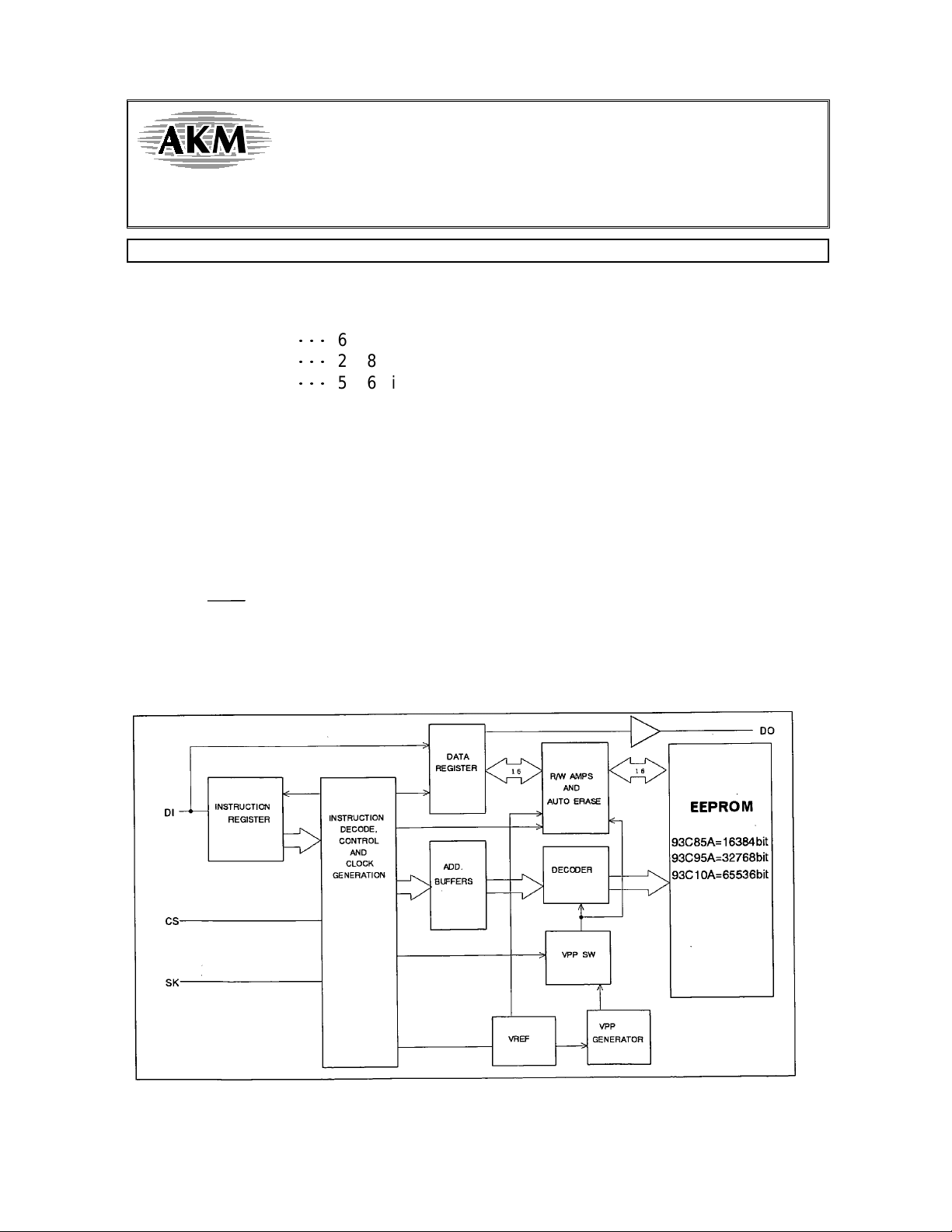
Block Diagram
DAM02E-01 1999/10
- 1 -
Page 2
ASAHI KASEI [AK93C85A/95A/10A]
General Description
The AK93C85A/95A/10A is a 16384/32768/65536-bit serial CMOS EEPROM divided into 1024/2048/4096
registers of 16 bits each. The AK93C85A/95A/10A has 4 instructions such as READ, WRITE, EWEN and
EWDS. Those instructions control the AK93C85A/95A/10A.
The AK93C85A/95A/10A can operate full function under wide operating voltage range from 1.8V to 5.5V. The
charge up circuit is integrated for high voltage generation that is used for write operation.
A serial interface of AK93C85A/95A/10A, consisting of chip select (CS), serial clock (SK), data-in (DI) and
data-out (DO), can easily be controlled by popular microcontrollers or standard microprocessors.
AK93C85A/95A/10A takes in the write data from data input pin (DI) to a register synchronously with rising
edge of input pulse of serial clock pin (SK). And at read operation, AK93C85A/95A/10A takes out the read
data from a register to data output pin (DO) synchronously with rising edge of SK.
The DO pin is usu all y in hig h impedan ce state. The DO pi n out pu t s "L" o r "H " i n case o f data ou tpu t o r Busy/R eady
signal output.
Software controlled write protection
When Vcc is applied to the part, the part automatically powers up in the ERASE/WRITE Disable state. In the
ERASE/WRITE disable state, execution of WRITE instruction is disa bled. Before WRITE instruction is
executed, EWEN instruction must be executed. The ERASE/WRITE enable state continues until EWDS
instruction is executed or Vcc is removed from the part.
Execution of a read instruction is independent of both EWEN and EWDS instructions.
Busy/Ready status signal
After a write instruction, the DO output serves as a Busy/Ready status indicator. After the falling edge of the
CS initiates the self-timed programming cycle, the DO indicates the Busy/Ready status of the chip if the CS is
brought high after a minimum of 250ns (Tcs). DO=logical "0" indicates that programming is still in progress.
DO=logical "1" indicates that the register at the address specified in the instruction has been written with the
new data pattern contained in the instruction and the part is ready for a next instruction.
The Busy/Ready status indicator is only valid when CS is active (high). When CS is low, the DO output goes
into a high impedance state.
The Busy/Ready signal outputs until a start bit (Logic"1") of the next instruction is given to the part.
Ty pe of Products
Model Memory size Temp.Range Vcc Package
AK93C85AF
AK93C85AM
AK93C95AF 32Kbits -40C85C1.8V
AK93C10AF 64Kbits -40C85C1.8V
16Kbits -40C85C
-40C85C
1.8V5.5V
1.8V5.5V
5.5V 8pin Plastic SOP
5.5V 8pin Plastic SOP
8pin Plastic SOP
8pin Plastic SSOP
DAM02E-01 1999/10
- 2 -
Page 3

ASAHI KASEI [AK93C85A/95A/10A]
Pin arrangement
Pin Name Function
CS Chip Select
SK Serial Data Clock
DI Serial Data Input
DO Serial Data Output
GND Ground
Vcc Power Supply
NC Not Connected
DAM02E-01 1999/10
- 3 -
Page 4
ASAHI KASEI [AK93C85A/95A/10A]
Functional Description
The AK93C85A/95A/10A has 4 instructions such as READ, WRITE, EWEN and EWDS. A valid instruction
consists of a Start Bit (Logic"1"), the appropriate Op Code and the desired memory Address location.
The CS pin must be brought low for a minimum of 250ns (Tcs) between each instruction when the instruction
is continuously executed.
Instruc-
tion
Start
BitOpCode
Address Data Comments
READ 1 10 A9-A0 D15-D0 Reads data stored in memory, at specified address.
WRITE 1 01 A9-A0 D15-D0 Writes register.
EWEN 1 00 11XXXXXXXX Write enable must precede all programming modes.
EWDS 1 00 00XXXXXXXX Disables all programming instructions.
WRAL 1 00 01XXXXXXXX D15-D0 Writes all registers.
table1. Instruction Set for the AK93C85A
Instruc-
tion
Start
BitOpCode
Address Data Comments
READ 1 10 A10-A0 D15-D0 Reads data stored in memory, at specified address.
WRITE 1 01 A10-A0 D15-D0 Writes register.
EWEN 1 00 11XXXXXXXXX Write enable must precede all programming modes.
EWDS 1 00 00XXXXXXXXX Disables all programming instructions.
WRAL 1 00 01XXXXXXXXX D15-D0 Writes all registers.
table2. Instruction Set for the AK93C95A
Instruc-
tion
Start
BitOpCode
Address Data Comments
READ 1 10 A11-A0 D15-D0 Reads data stored in memory , at specified address.
WRITE 1 01 A11-A0 D15-D0 Writes register.
EWEN 1 00 11XXXXXXXXXX Write enable must precede all programming modes.
EWDS 1 00 00XXXXXXXXXX Disables all programming instructions.
WRAL 1 00 01XXXXXXXXXX D15-D0 Writes all registers.
table3. Instruction Set for the AK93C10A
(Note)
The WRAL instruction are used for factory function test only.
User can't use the WRAL instruction.
The AK93C85A/95A/10A perceives the start bit in the logic"1" and also "01".
DAM02E-01 1999/10
- 4 -
Page 5

ASAHI KASEI [AK93C85A/95A/10A]
Write
The write instruction is followed by 16 bits of data to be written into the specified address.
AK93C85A : After the last bit of data is put on the DI pin, the CS pin must be brought low
before the next rising edge of the SK clock. This falling edge of the CS initiates the self-timed programming
Busy
cycle. The DO indicate s the
(Tcs).
AK93C95A/10A : The self-timed programming cycle is initia ted on the rising edge of the SK
clock as the last data bit (D0) is clocked in. The DO indicates the
timed programming cycle is initiated.
Busy
The
into a high impedance state. The
is given to the part.
DO=logical "0" indicates that programming is still in progress. DO=logical "1" indicates that t he register at the
address specified in the instruction has been written with the new data pattern contained in the instruction and
the part is ready for a next instruction.
/Ready status indicator is only valid when CS is active (high). When CS is low, the DO output goes
/Ready status of the chip if the CS is brought high after a minimum of 250ns
Busy
/Ready status of the chip after the self-
Busy
/Ready signal outputs until a start bit (Logic"1") of the next instruction
DAM02E-01 1999/10
- 5 -
Page 6

ASAHI KASEI [AK93C85A/95A/10A]
Read
The read instruction is the only instruction which outputs serial data on the DO pin.
Following the Start bit, first Op code and address are decoded, then the data from the selected memory
location is available at the DO pin. A dummy bit (logical "0") precedes the 16-bit data from the selected
memory location. The output data changes are synchronized with the rising edges of the serial clock (SK).
The data in the next address can be read sequentially by continuing to provide clock. The address
automatically cycles to the next higher address after the 16bit data shifted out.
AK93C85A
When the highest address is reached ($3FF), the address counter rolls over to
address $000 allowing the read cycle to be continued indefinitely.
AK93C95A
When the highest address is reached ($7FF), the address counter rolls over to
address $000 allowing the read cycle to be continued indefinitely.
AK93C10A
When the highest address is reached ($FFF), the address counter rolls over to
address $000 allowing the read cycle to be continued indefinitely.
DAM02E-01 1999/10
- 6 -
Page 7

ASAHI KASEI [AK93C85A/95A/10A]
EWEN / EWDS
When Vcc is applied to the part, the part automatically powers up in the ERASE/WRITE Disable state. In the
ERASE/WRITE disable state, execution of WRITE instruction is disable. Before WRITE instruction is
executed, EWEN instruction must be executed. The ERASE/WRITE enable state continues until EWDS
instruction is executed or Vcc is removed from the part.
Execution of a read instruction is independent of both EWEN and EWDS instructions.
DAM02E-01 1999/10
- 7 -
Page 8

ASAHI KASEI [AK93C85A/95A/10A]
Absolute Maximum Ratings
Parameter Symbol Min Max Unit
Power Supply VCC -0.6 +7.0 V
All Input Voltages
VIO -0.6 VCC+0.6 V
with Respect to Ground
Ambient storage temperature Tst -65 +150
C
Stress above those listed under "Absolute Maximum Ratings" may cause permanent
damage to the device. This is a stress rating only and functional operation of the device at
these or any other conditions above those indicated in the operational sections of the
specification is not implied. Exposure to absolute maximum conditions for extended
periods may affect device reliability.
Recommended Operating Condition
Parameter Symbol Min Max Unit
Power Supply VCC 1.8 5.5 V
Ambient Operating Temperature Ta -40 +85
C
DAM02E-01 1999/10
- 8 -
Page 9

ASAHI KASEI [AK93C85A/95A/10A]
Electrical Characteristics
(1) D.C. ELECTRICAL CHARACTERISTICS
( 1.8VVcc5.5V, -40CTa85C, unless otherwise specified )
Parameter Symbol Condition Min. Max. Unit
ICC1 VCC=5.5V, tSKP=1us, *1 5.5 mACurrent Dissipation
(WRITE)
ICC2 VCC=1.8V, tSKP=4us, *1 3.0 mA
ICC3 VCC=5.5V, tSKP=1us, *1 0.4 mACurrent Dissipation
(READ,EWEN,EWDS)
Current Dissipation
ICC4 VCC=1.8V, tSKP=4us, *1 0.1 mA
SB
ICC
VCC=5.5V *2 0.8 uA
(Standby)
Input High Voltage VIH 0.8 VCC VCC+0.5 V
Input Low Voltage VIL -0.1 0.2 VCC V
VOH1 2.5VVCC5.5V
0.8 VCC VOutput High Voltage
IOH=-0.1mA
VOH2 1.8VVCC<2.5V
0.8 VCC V
IOH=-0.1mA
VOL1 2.5VVCC5.5V
0.4 VOutput Low Voltage
IOL=1.0mA
VOL2 1.8VVCC<2.5V
0.4 V
IOL=0.1mA
Input Leakage ILI VCC=5.5V,VIN=5.5V
1.0 uA
Output Leakage ILO VCC=5.5V
VOUT=5.5V,CS=GND
*1:VIN=VIH/VIL,DO=Open
*2:VIN=VCC/GND,CS=GND,DO=Open
1.0 uA
DAM02E-01 1999/10
- 9 -
Page 10

ASAHI KASEI [AK93C85A/95A/10A]
(2) A.C. ELECTRICAL CHARACTERISTICS
( 1.8VVcc5.5V, -40CTa85C, unless otherwise specified )
Parameter Symbol Condition Min. Max. Unit
SK Cycle Time
tSKP1 4.5VVCC5.5V 1.0 us
tSKP2 2.0VVCC<4.5V 2.0 us
tSKP3 1.8VVCC<2.0V 4.0 us
SK Pulse Width
tSKW1 4.5VVCC5.5V 500 ns
tSKW2 2.0VVCC<4.5V 1.0 us
tSKW3 1.8VVCC<2.0V 2.0 us
CS Setup Time tCSS 100 ns
CS Hold Time tCSH 0 ns
Data Setup Time tDIS 200 ns
Data Hold Time tDIH 200 ns
Output delay
tPD1 4.5VVCC5.5V, *3 500 ns
tPD2 2.0VVCC<4.5V, *3 1.0 us
tPD3 1.8VVCC<2.0V. *3 2.0 us
tE/W1 4.5VVCC5.5V 8 msSelftimed Programming
Time
tE/W2 1.8VVCC<4.5V 10 ms
Min CS Low Time tCS 250 ns
CS to Status Valid1 tSV CL=100pF 500 ns
CS to Status Valid2 tSVV CL=100pF 1000 ns
tOZ1 2.0VVCC5.5V 100 nsCS to Output High-Z
tOZ2 1.8VVCC<2.0V 250 ns
*3:CL=100pF
DAM02E-01 1999/10
- 10 -
Page 11

ASAHI KASEI [AK93C85A/95A/10A]
Synchronous Data timing
The Start of Instruction
The End of Instruction
DAM02E-01 1999/10
- 11 -
Page 12

ASAHI KASEI [AK93C85A/95A/10A]
Busy/Ready Signal Output (AK93C85A)
Busy/Ready Signal Output (AK93C95A/10A)
DAM02E-01 1999/10
- 12 -
Page 13

IMPORTANT NOTICE
z These products and their specifications are subject to change without notice. Before
considering any use or application, consult the Asahi Kasei Microsystems Co., Ltd. (AKM)
sales office or authorized distributor concerning their current status.
z AKM assumes no liability for infringement of any patent, intellectual property, or other
right in the application or use of any information contained herein.
z Any export of these products, or devices or systems containing them, may require an
export license or other official approval under the law and regulations o f the country of
export pertaining to customs and tariffs, currency exchange, or strategic materials.
z AKM products are n either intended nor authorized for use as critical co mponents in any
safety, life support, or other hazard related device or system, and AKM assumes no
responsibility relating to any such use, except with the express written consent of the
Representative Director of AKM. As used here:
(a) A hazard related device or system is one designed or intended for life support or
maintenance of safety or for applications in medicine, aerospace, nuclear ener gy, or
other fields, in which its failure to function or perf orm may reasonably be expected to
result in loss of life or in significant injury or damage to person or property.
(b) A critical component is one whose failure to func tion or perform may reasonably be
expected to result, whether directly or indirectly, in the loss of the safety or
effectiveness of the device or system containing it, and which must therefore meet
very high standards of performance and reliability.
z It is the responsibility of the buyer or distributor of an AKM product who distributes,
disposes of, or otherwise places the product with a third party to notify that party in
advance of the above content and conditions, and the buyer or distributor agrees to
assume any and all re sponsibility and liability for and ho ld AKM harmless fr om any and
all claims arising from the use of said product in the absence of such notification.
 Loading...