

Page 1
ASAHI KASEI [AK7712A-VT]
AK7712A-VT
Built-in 20-bit ADC/DAC Sophisticated Audio DSP
General Description
The AK7712A is a DSP(Digital Signal Processor) with built-in high performance 20bit 2ch ADC and 4ch DAC, on
purposeto control the sound field. It is possible to calculate 383 steps on 44.1kHz and 48kHz sampling respectively.
In case of 32kHz sampling, it can caluculate up to 511 steps. With a combination of this LSI and external memory
for delay data,it can berealized easily to control the sound field such as Echo, Surround Presence Controller, and
Key-control which are needed forsomething like Karaoke. Parametric Equalizing can be done without external
memory.
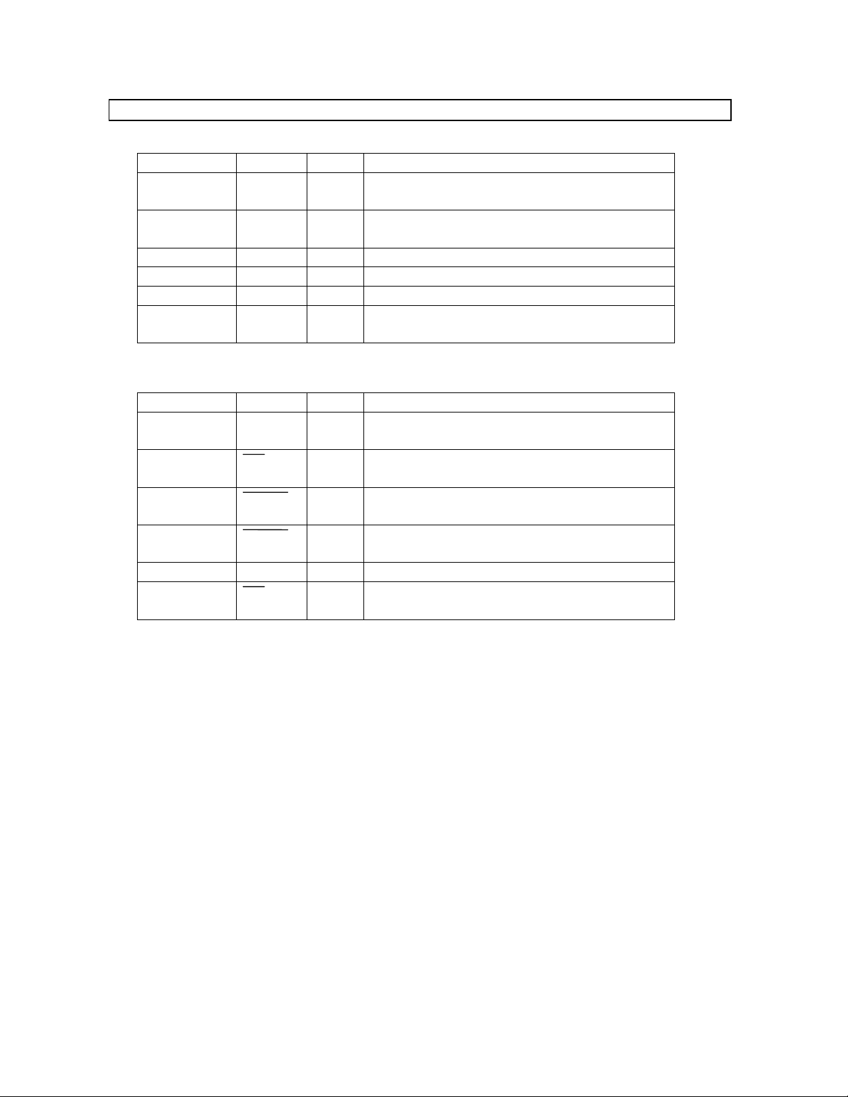
Features
[ DSP unit ]
Word length: 24-bit (data RAM)
Instruction cycle time: 54ns(maximum speed)
Multiplier: 24 × 16 → 40-bit
Divider: 16 ÷ 16 → 16-bit
Program RAM: 384 × 32 bit
External memory: DRAM,Pseudo-SRAM and SRAM can be connected (only use for delay data).
Sampling frequency: 32kHz∼48kHz
Automatic clear function of external RAM:
47msec after bringing RST high at fs=48kHz (include internal data RAM)
Microcomputer interface:
synchronized signal type 8-bit serial input 1 channel,
synchronized signal type 24-bit serial output 1 channel
Master clock: 512(511)/384(383)/256(255)fs
The value inside ( ) is maximum calculation steps.
512fs mode is available when 32kHz sampling is chosen.
Conversion of master/slave mode for LRCK and BCLK:
When master mode is selected, the outputs of LRCK and BCLK depend
on the set-up for input format.
Serial input ports(2~4ch), and output ports(2~6ch) : 16/20/24 bit words
[ ADC unit ]
20-bit 64 × Oversampling ∆Σ ADC: 2ch
S/(N+D): 92dB
DR, S/N: 98dB
[ DAC unit ]
20-bit 128 × Oversampling ∆Σ DAC: 4ch
S/(N+D): 86dB
DR, S/N: 97dB
Digital HPF (fc=1Hz)
[ Total ]
Power supply: +5V
Package: 100pin LQFP(0.5mm pitch)
0180-E-02 1997/12
- 1 -
Page 2

ASAHI KASEI [AK7712A-VT]
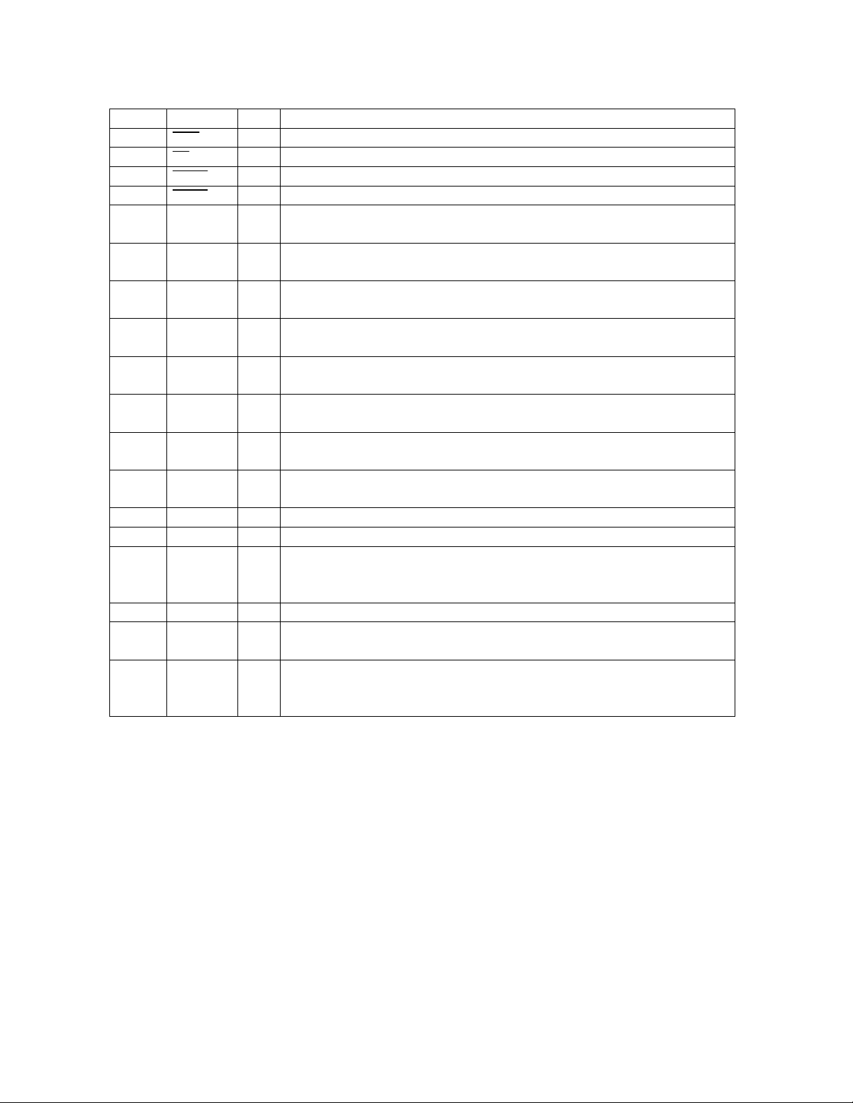
Detail Features
1) Calculate Unit
•
Multiplication: 24-bit × 16-bit→ 40-bit(fixed-point, 2 instruction cycle time)
•
Division: 16-bit ÷ 16-bit→ 16-bit(fixed-point, 17 instruction cycle time)
•
ALU: 34-bit arithmetic operation
24-bit arithmetic logic operation
•
Shift: 1-,2-,3-,4-,6-,8-,15-bit right/left shift
AK7712A has indirect shift function.
(A shift using DBUS data can not use DBUS
as multiplication input.)
•
Register: 34-bit × 4(ACC) [for ALU]
24-bit × 8(TMP) [for DBUS connection]
•
Double precision operation:
24-bit(data)×31-bit(coefficient), 45 × 31, 45 × 16
2) Internal Memory
•
Program RAM: 384 word × 32-bit
•
Data RAM: 128 word × 24-bit
•
Coefficient RAM: 256 word × 16-bit
•
Offset RAM: 40 word × 16-bit (for external memory access)
•
Microcomputer buffer: 16 word × 16-bit
3) External Memory Access (SRAM
•
Objective memory: 256k(32k × 8-bit),1M(128k × 8-bit) × 1 / SRAM
•
Pseudo-SRAM•DRAM)
256k(32k × 8-bit),1M(128k × 8-bit) × 1 / Pseudo-SRAM
256k(64k × 4-bit),1M(256k × 4-bit) × 2 or × 1 / DRAM
(Half volume of 1M DRAM is used as 512k memory.)
•
Treating bit length: 16-bit (24-bit is available, but double time is needed for access.)
•
The number of times to access:
SRAM, 256k Pseudo-SRAM ; 76 at 384fs
: DRAM, 1M Pseudo-SRAM ; 64 at 384fs (32 at one DRAM)
: SRAM, 256k Pseudo-SRAM ; 51 at 256fs
: DRAM, 1M Pseudo-SRAM ; 42 at 256fs (21 at one DRAM)
•
Memory access time:
less than 100nsec
•
Maximum address length:
65535 sampling times (at 1M SRAM)
2.048sec at 32kHz, 1.486sec at 44.1kHz, 1.365sec at 48kHz
4) Input/Output Port
•
Input: 2ch analog input: 20-bit ADC, DR=98dB (16-bit at BCLK=32fs)
[when built-in ADC is connected.]
2ch digital input: MSB justified 20-bit (16bit at BCLK=32fs)
…
MSB first serial input
[when built-in ADC is isolated.]
2ch digital input: MSB justified 16-
•
Output: 4ch analog output: 20-bit DAC, DR=97dB(16-bit at BCLK=32fs)
•
24-bit / LSB justified 16-•24-bit
…
MSB first serial input
[when built-in ADC is connected.]
4ch digital output: MSB justified 20-bit (16bit at BCLK=32fs)
…
MSB first serial output
[when built-in ADC is isolated.]
2ch digital output: MSB justified 16-
•
24-bit/ LSB justified 16-bit
…
MSB first serial output
5) Cascade connection with this LSI is possible.
6) Interface to Microcomputer:
synchronized 8-bit serial input / synchronized 24-bit serial output
7) Calculation Cycle: max 18.432MHz(54nsec) [at 48.0kHz, 384fs, 5V]
8) Master/Slave conversion of LRCK
BCLK is possible.
9) BCLK: 32fs/48fs/64fs (64fs only at master mode)
0180-E-02 1997/12
- 2 -
Page 3

ASAHI KASEI [AK7712A-VT]
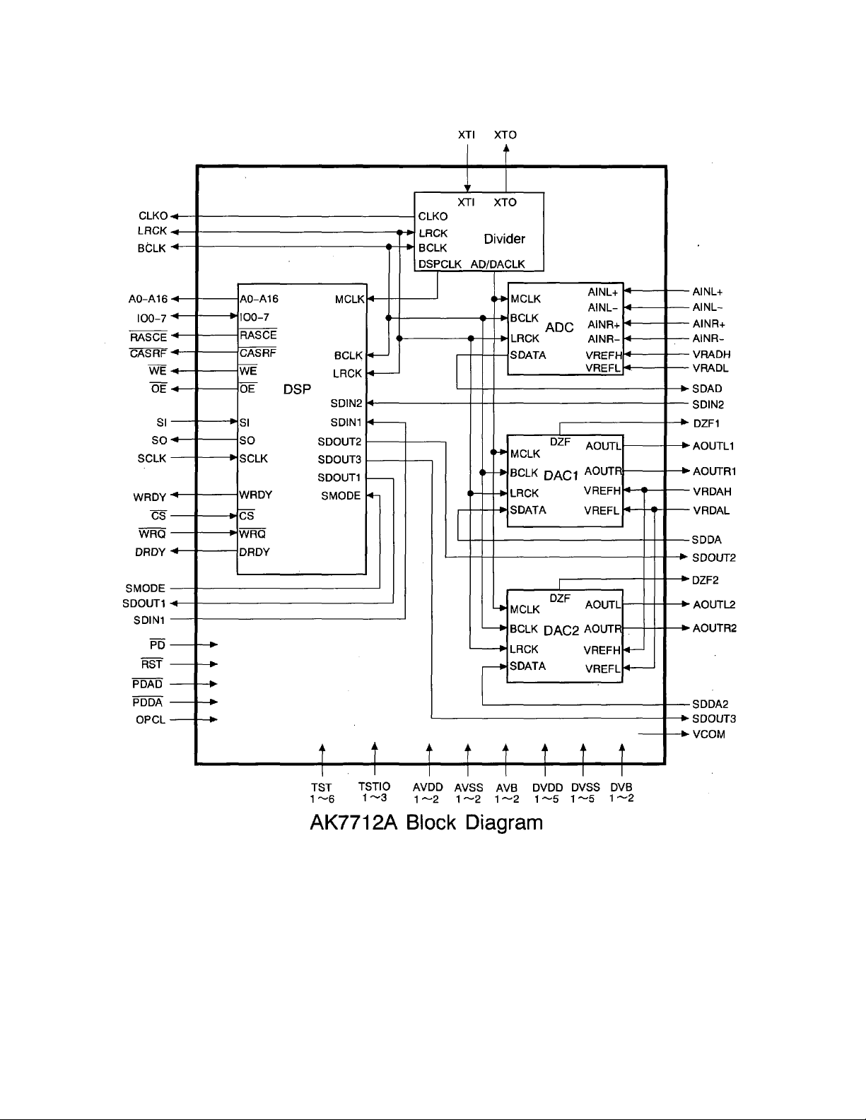
AK7712A Block Diagram
1) ADC,DAC Inside Connection Mode (OPCL: L)
AK7712A Block Diagram
Note: Please use SDIN2,SDDA and SDDA2 with "L" or open.
SDAD,SDOUT2 and SDOUT3 output "L".
0180-E-02 1997/12
- 3 -
Page 4
ASAHI KASEI [AK7712A-VT]
2) ADC,DAC Outside Connection Mode (built-in ADC,DAC isolation mode) (OPCL:H)
0180-E-02 1997/12
- 4 -
Page 5
ASAHI KASEI [AK7712A-VT]
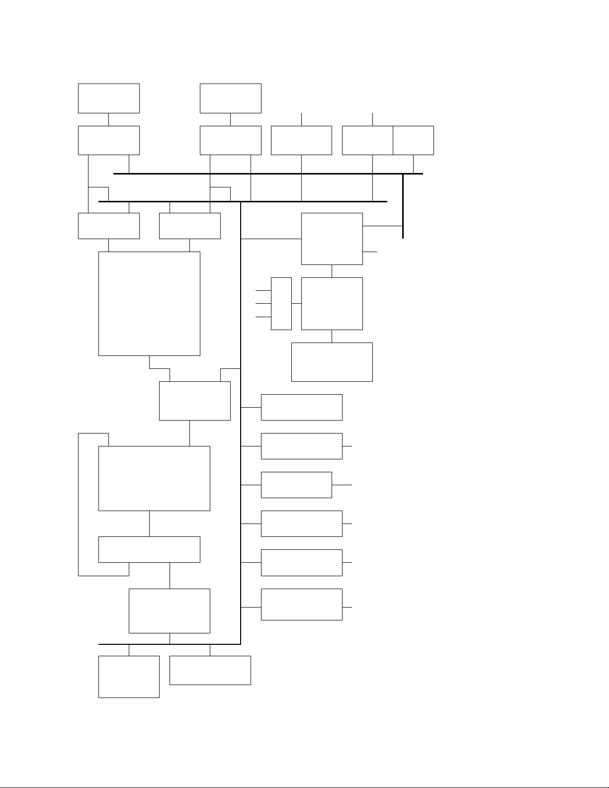
AK7712A DSP unit Block Diagram
Data Address
CP0,1 DP0,1
CRAM
256 × 16
CBUS (16-bit)
DBUS (24-bit)
MPX16 MPX24
X Y
Multiply
16 × 24→40
40-bit
DRAM
128 × 24
24-bit
D0a7 AD0a16
Delay Data
16-bit
Micom I/F
Control
D
E
C
PRAM
384 × 32
PC
Stack:1Level
Ext RAM
Control
Interface
OFRAM
40 × 16
Microcomputer Serial
34-bit
MUL DBUS
SHIFT
34-bit
A B
ALU
34-bit
Overflow Margin:4bit
DR0a3
24-bit
Overflow Data
Generator
Division
16 ÷ 16→16
Peak Detector
TMP 8 × 24-bit
2 × 24/16-bit
2 × 20/16-bit
2 × 24/16-bit
2 × 20/16-bit
2 × 20/16-bi
note 1: Normally it's connected to built-in ADC
2: Normally it's connected to built-in DAC1
3: Normally it's connected to built-in DAC2
SDIN1 (24/16-bit)
MSB/LSB justified Serial In
SDIN2 (20/16-bit)
MSB justified Serial In (note 1)
SDOUT1 (24/16-bit)
MSB/LSB justified Serial Out
SDOUT2 (20/16-bit)
MSB justified Serial Out (note 2)
SDOUT3 (20/16-bit)
MSB justified Serial Out (note 3)
0180-E-02 1997/12
- 5 -
Page 6
ASAHI KASEI [AK7712A-VT]
Ordering Guide
AK7712A-VT -40∼+85°C 100pin LQFP
AKD7712A Evaluation Board
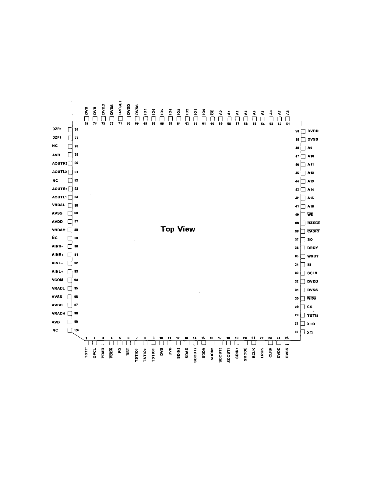
Pin Layout
0180-E-02 1997/12
- 6 -
Page 7
ASAHI KASEI [AK7712A-VT]
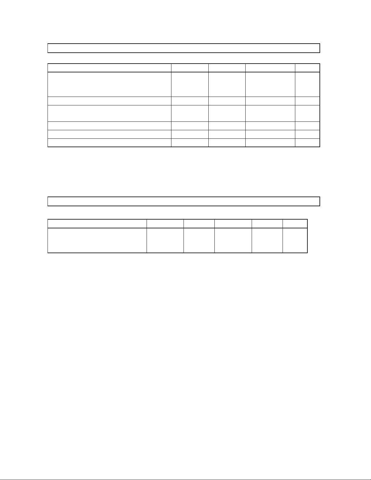
Pin / Function
Power Supply
Pin No. Pin name I/O Function
24, 32, 50,
70, 73
25, 31, 49,
69, 72
87, 97 AVDD - Analog power supply
86, 96 AVSS - Analog ground
79, 99 AVB - Analog substrate power supply
10, 11, 74,
75
External RAM Interface Signal
Pin No. Pin name I/O Function
41∼48,
51∼59
40 WE O Write signal output
39 RESCE O RAS for external DRAM
38 CASRF O CAS for external DRAM
61∼68 IO0∼IO7
60 OE O Output enable signal output
DVDD - Digital power supply
DVSS - Digital ground
DVB - Digital substrate power supply
A16∼A0
O Address output for external RAM
(A0:LSB justified, A16:MSB justified)
for external SRAM/ Pseudo-SRAM/ DRAM
/ Pseudo-SRAM-CE
/ Pseudo-SRAM refresh
I/O Data input/output for external RAM
for external SRAM/ Pseudo-SRAM/ DRAM
0180-E-02 1997/12
- 7 -
Page 8

ASAHI KASEI [AK7712A-VT]
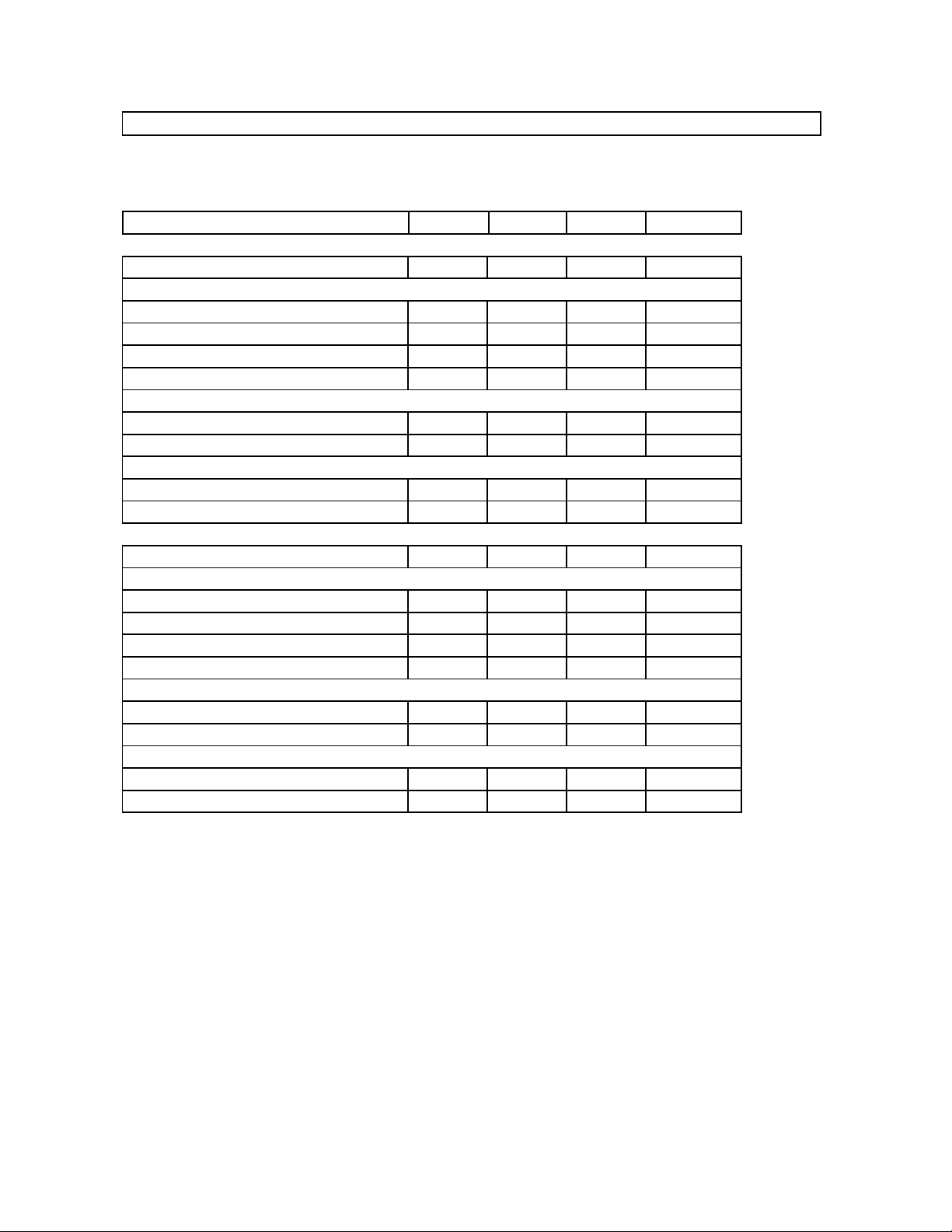
Microcomputer Interface Signal, Controls Signal, Input/Output Data, Reset, etc.
Pin No. Pin name I/O Function
30 WRQ I Command register reset input
for microcomputer interface
33 SCLK I Clock input for serial data input
for microcomputer interface
36 DRDY O Output data ready output
for microcomputer interface
34 SI I Serial data input
for microcomputer interface
37 SO O Serial data output
for microcomputer interface
(Hi-Z state at CS="H")
35 WRDY O Data write ready output
for microcomputer interface
(Hi-Z state at CS="H")
29 CS I Chip select input
for microcomputer interface
0180-E-02 1997/12
- 8 -
Page 9
ASAHI KASEI [AK7712A-VT]
AK7712A Control Signal, Input/Output Data Signal, Reset, etc.
Pin No Pin name I/O Function
6 RST I Reset input ("L" Reset) (note 1)
5 PD I Power down (note 1)
3 PDAD I AD reset control (note 1)
4 PDDA I DA reset control (note 1)
19 SDIN1 I Serial data input 1
•
MSB justified 16-
24-bit / LSB justified 16-•24-bit
18 SDOUT1 O Serial data output 1
•
MSB justified 16-
24-bit / LSB justified 16-bit
12 SDIN2 I Serial data input 2 (OPCL : "H" ) (note 2)
•
MSB justified 16-
20-bi
13 SDAD O Serial data output 2 (OPCL : "H" ) (note 3)
•
MSB justified 16-
20-bit, common set-up with SDIN2
15 SDDA I Serial data input 3 (OPCL : "H" ) (note 2)
MSB justified 16-
•
20-bit, common set-up with SDOUT2
14 SDOUT2 O Serial data output 3 (OPCL : "H" ) (note 3)
•
MSB justified 16-
20-bit
16 SDDA2 I Serial data input 4 (OPCL : "H" ) (note 2)
MSB justified 20-bit (16-bit at BCLK=32fs )
17 SDOUT3 O Serial data output 4 (OPCL : "H") (note 3)
MSB justified 20-bit (16-bit at BCLK=32fs)
21 BCLK I/O Clock input/output for serial data input
22 LRCK I/O L/R channel identify signal input/output
Interface clock select
20 SMODE I
Input/output set-up for each clock pin of LRCK and BCLK
"L":slave mode(21,22 input), "H":master mode(output)
23 CLKO O Master clock output (note 4)
27 XTO O Output for quartz oscillator
When an external clock is input, this pin should be left floating.
26 XTI I Input for quartz oscillator
A crystal can be connected between this pin and XTO, or an external CMOS
clock can be input on this pin.
note:1 About the directions, please refer the paragraph of power down reset control on P.65.
2 Set to "L" or "open" when OPCL is "L".
3 The output is "L" when OPCL is "L".
4 During a timing of changing CONTROL REGISTER, CLKO is instability.
0180-E-02 1997/12
- 9 -
Page 10
ASAHI KASEI [AK7712A-VT]
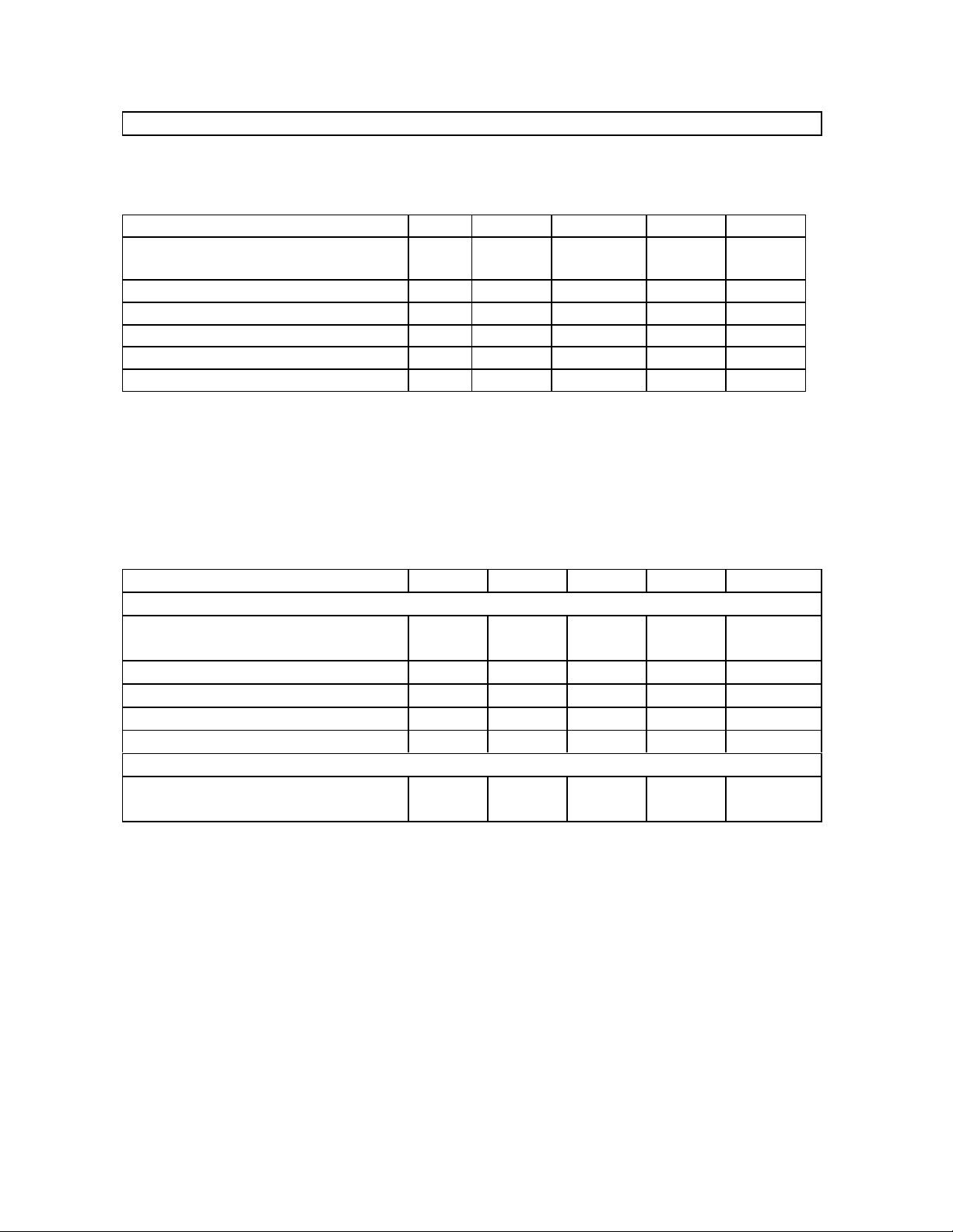
Analog Relational Pins
Pin No. Pin name I/O Function
93 AINL+ I ADC Lch analog non-inverted input
92 AINL- I ADC Lch analog inverted input
91 AINR+ I ADC Rch analog non-inverted input
90 AINR- I ADC Rch analog inverted input
84 AOUTL1 O DAC1 Lch analog output 1
83 AOUTR1 O DAC1 Rch analog output 1
81 AOUTL2 O DAC2 Lch analog output 2
80 AOUTR2 O DAC2 Rch analog output 2
85 VRDAL I Standard voltage input of DAC unit
(normally connected to analog ground)
88 VRDAH I Standard voltage input of DAC unit
(normally connected to 87 pin.
0.1u and 10uF capacitor are connected
between this pin and VRDAL pin.)
95 VRADL I Standard voltage input of ADC unit
(normally connected to analog ground)
98 VRADH I Standard voltage input of ADC unit
(normally connected to 97 pin.
0.1u and 10uF capacitor are connected
between this pin and VRADL pin.)
94 VCOM O Common voltage
(0.1u and 10uF capacitor are connected
between this pin and analog ground.)
0180-E-02 1997/12
- 10 -
Page 11
ASAHI KASEI [AK7712A-VT]
Test Pin, etc.
Pin No. Pin name I/O Function
77 DZF1 O Zero input find (for DAC1)
76 DZF2 O Zero input find (for DAC2)
1 TSTI1 I Test input 1 ; use as "L" or open
28 TSTI2 I "L": CLKO(23pin) output
"H": CLKO(23pin)→"L"
7 TSTIO1 I/O Test input 1 ; use as "L" or open
8 TSTIO2 I/O Test input 2 ; use as "L" or open
9 TSTIO3 I/O Test input 3 ; use as "L" or open
2 OPCL I ADC,DAC connection choice
"L": connect , "H": separate
71 DZFSET I Zero point find set
"H": DZF output , "L": DZF output→"L"
78, 82,
89, 100
NC - NC pins do not be bonded inside.
0180-E-02 1997/12
- 11 -
Page 12
ASAHI KASEI [AK7712A-VT]
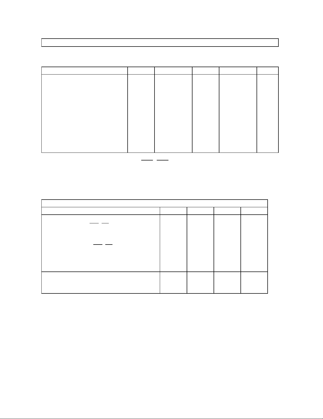
Absolute Maximum Ratings
(AVSS,DVSS=0V; note 1)
Parameter Symbol min max Unit
DC Power supply: analog power
digital power(DVDD) (note 2)
substrate power(AVB,DVB)
Input current (except power supply) IIN Analog input voltage
AINL+,AINL-,AINR+,AINR-,VREF
Digital input voltage (note 2) VIND -0.3 (VB)+0.3 V
Ambient temperature Ta -40 85
Storage temperature Tstg -65 150
note 1: All the value mean the voltage against the ground pin.
2: Maximum absolute value must be within 6.0V, i.e. VB+0.3V ≤ 6.0V.
Warning: To operate beyond these limits may result in permanent damage to the device.
Normal operation is not guaranteed at these extremes.
VA
VD
VB
VINA
-0.3
-0.3
-0.3
-0.3 (VA)+0.3 V
6.0
(VB)+0.3
6.0
10
±
mA
°
°
V
V
V
C
C
Recommended Operating Conditions
(AVSS,DVSS=0V; note 1)
Parameter Symbol min typ max Unit
Power supply: analog power
digital power (DVDD)
substrate power (AVB,DVB)
(note 2,3,4)
note 1: All the value mean the voltage against the ground pin.
2: The VA and VB should be powered at the same time or earlier than VD.
3: The VA and VB are connected together through the chip substrate and has several ohms resistors.
The VA and VB should be supplied from the same power unit.
4: Analog input/output voltages are proportional to the voltages of VRADH,VRDAH.
* AKM assumes no responsibility for the usage beyond the conditions in this data sheet.
VA
VD
VB
4.75
4.75
4.75
5.0
5.0
5.0
5.25
VB
5.25
V
V
V
0180-E-02 1997/12
- 12 -
Page 13
ASAHI KASEI [AK7712A-VT]
Analog Characteristics
(Ta=25°C; AVDD,DVDD,AVB,DVB=5.0V; VRADH=AVDD,VRADL=AVSS,VRDAH=AVDD,VRDAL=AVSS;
fs=44.1kHz; BCLK=64fs master mode; MCLK=256fs; input signal frequency=1kHz; 20-bit;
measurement band width=10Hz∼20kHz; DSP unit is reset; ADC differential input; unless otherwise specified.)
Parameter min typ max Units
ADC unit :
Resolution 20 Bits
Dynamic characteristics
S/(N+D) ( -0.5dB ) 86 92 dB
S/N (A-Weight) 94 98 dB
Dynamic range (A-Weight) (note 1) 94 98 dB
Interchannel isolation (f=1kHz) 90 105 dB
DC Accuracy
Interchannel gain mismatch 0.1 0.3 dB
Gain drift - 50 Analog input
1.9
Input voltage (note 2)
Input impedance 220
DAC unit :
Resolution 20 Bits
Dynamic characteristics
S/(N+D) ( 0 dB ) 80 86 dB
S/N (A-Weight) 93 97 dB
Dynamic range (A-Weight) (note 1) 93 97 dB
Interchannel isolation (f=1kHz) (note 4) 90 105 dB
DC Accuracy
Interchannel gain mismatch (note 4) 0.2 0.5 dB
Gain drift - 50 Analog output
Output voltage (note 3) 2.65 2.90 3.15 Vp-p
Load resistance 5
note 1: S/(N+D) with an input signal of -60dB below full-scale.
2: The full-scale of analog input voltage(AIN = (AIN+) - (AIN-) ) equals to
FS = ±(VRADH - VRADL) × 0.4
±
3: The full-scale of output voltage(0dB) is proportional to VRDAH.
Aout(typ. @0dB) = 2.9Vpp × VRDAH/5
4: Between L channel and R channel of each DAC.
±
2.0
±
2.1
±
ppm/°C
Vp-p
k
Ω
ppm/°C
k
Ω
0180-E-02 1997/12
- 13 -
Page 14
ASAHI KASEI [AK7712A-VT]
Digital Filter Characteristics
This data is not the guaranteed characteristic value but the designed value as a reference.
ADC unit :
(Ta=25°C; VA,VD,VB=5.0V±5%; fs=44.1kHz)
Parameter Symbol min typ max Units
Passband (±0.06dB)
( -6.0 dB) (note 1)
Stopband (note 1) SB 24.35 kHz
Passband ripple (note 2) PR
Stopband attenuation (note 3,4) SR 80 dB
Group delay distortion
Group delay (Ts=1/fs) GD 29.3 Ts
note 1: The frequencies of passband/stopband are proportional to the sampling frequency (fs).
2: Passband is DC to 19.75kHz at fs=44.1kHz.
3: Stopband is 27.56kHz to 2.795MHz at fs=44.1kHz.
4: The analog modulator samples the input at 2.8224MHz for fs=44.1kHz. There is no rejection of
input signals at those band width which are multiples of the sampling frequency(n x 2.8224MHz
±20.21kHz; n=0,1,2,3…).
PB 0
GD
∆
20.00
0
22.05
0.005 dB
±
0us
kHz
kHz
DAC unit :
(Ta=25°C; VA,VD,VB=5.0V±5%; fs=44.1kHz;)
Parameter Symbol min typ max Units
Digital filter
Passband ( -0.2 dB) (note 1)
( -6.0 dB)
Stopband (note 1) SB 24.3 kHz
Passband ripple PR
Stopband attenuation SA 41 dB
Group delay (Ts = 1/fs) (note 2) GD - 14.7 - Ts
Digital filter + analog filter
Amplitude characteristics
0∼20kHz
note 1: The frequencies of passband/stopband are proportional to the sampling frequency (fs);
PB=0.4535fs(@-0.2dB), SB=0.546fs(@-41dB).
2: The calculating delay time is occurred by digital filtering. This is the time from the setting
20-bit data on input register to the output of analog signal. (at fs=44.1kHz)
PB 0
- 22.05
-
0.5 - dB
±
20.0
-
0.05 dB
±
kHz
kHz
0180-E-02 1997/12
- 14 -
Page 15
ASAHI KASEI [AK7712A-VT]
DC Characteristics
(AVDD=DVDD; AVD,DVB=5.0V±5%; Ta=25°C)
Parameter Symbol min typ max Units
High level input voltage
Low lev e l input voltage
VIH
VIL
70%VDD
-
-
-
-
30%VDD
V
V
High level input voltage
Iout=-20uA
Low lev e l input voltage
Iout= 20uA
Input leak current (note 1)
Input leak current (note 2)
(pull-down pin)
note 1: except pull-up/pull-down pin
2: Pull-down pin(Typ 50kΩ) is as follows; PDAD, PDDA,SDIN2,SDDA,SDDA2,TSTI1,TSTI2,
TSTO1,TSTO2,TSTO3,OPCL pin.
(Ta=25°C; AVDD,DVDD,AVB,DVB=5.0V; Master clock = 18.432MHz, XTI=384fs [fs=48kHz]; Input 1kHz full scale
sine wave input from 2ch analog input pin of ADC and output to 4ch DAC.)
Power supply
Parameter min typ max Units
Power supply current
Normal operation (RST=PD="H")
AVDD + AVB + DVB
DVDD
Power-down mode (RST=PD="L")
AVDD + AVB + DVB+ DVDD (note 3)
VOH
VOL
Iin
Iid
VDD-0.1
-
-
-
47
51
20
-
-
-
100
70
80
250
0.1
±
-
10
-
V
V
uA
uA
mA
mA
uA
Power dissipation
Normal operation
Power-down mode
note 3: This is the value in the conditions that external clock(XTI,BCLK,LRCK) is "L", SCLK is "H".
0180-E-02 1997/12
- 15 -
490
0.1
750
1.25
mW
mW
Page 16
ASAHI KASEI [AK7712A-VT]
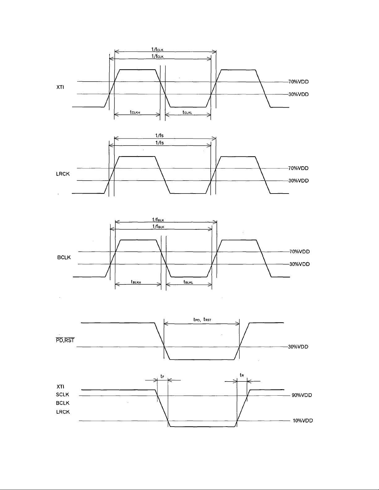
Switching Characteristics
••••
Clock
(Ta=25°C; VA,VD,VB=5.0V±5%; C
=20pF)
L
Parameter Symbol min typ max Units
Control clock frequency
Master clock
Quartz oscillator mode
256fs:
384fs:
512fs:
f
CLK
f
CLK
f
CLK
8.192
12.288
12.288
11.2896
16.9344
16.384
12.288
18.432
18.432
MHz
MHz
MHz
External clock mode
Duty cycle
256fs:
Pulse width Low
Pulse width High
384fs:
Pulse width Low
Pulse width High
512fs:
Pulse width Low
Pulse width High
Audio serial data clock (BCLK)
Channel select clock (LRCK)
Duty cycle
Microcomputer serial data clock (SCLK
Pulse width Low
Pulse width High
f
t
t
f
t
t
f
t
t
f
f
f
t
t
CLK
CLKL
CLKH
CLK
CLKL
CLKH
CLK
CLKL
CLKH
BLK
S
SLK
SLKL
SLKH
40
8.192
30
30
12.288
20
20
12.288
20
20
1.024
32
49
30
30
50
11.2986
16.9344
16.384
2.8224
44.1
50
60
12.288
18.432
18.432
3.072
48
51
12.288
%
MHz
ns
ns
MHz
ns
ns
MHz
ns
ns
MHz
kHz
%
MHz
ns
ns
Reset timing
PD pulse width
RST pulse width
t
PD
t
RST
100
100
ns
ns
Clock falling time
[XTI, BICK, LRCK, SCLK] (note)
Clock rising time
[XTI, BICK, LRCK, SCLK] (note)
t
f
10
t
r
10
ns
ns
note : At input of external CMOS clock for XTI.
0180-E-02 1997/12
- 16 -
Page 17
ASAHI KASEI [AK7712A-VT]
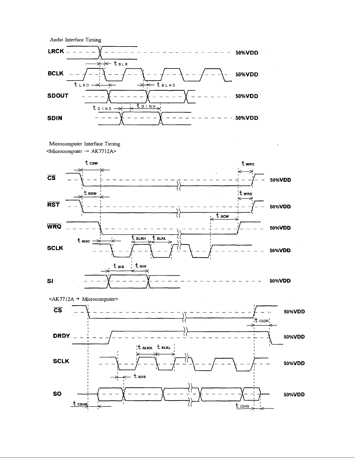
1) Audio Interface Timing
(AVDD=DVDD,AVB,DVB=5.0V±5%,Ta=25°C;
Master clock 16.9344MHz,XTI=384fs[fs=44.1kHz]; CL=20pF)
Parameter Symbol min typ max Units
Slave mode
BCLK cycle
BCLK pulse width Low
pulse width High
Time from BCLK"↓" to LRCK (note 1)
Delay time from LRCK to DOUT(MSB)
Delay time from BCLK"↓" to DOUT
Latch hold time of SDIN
Latch setup time of SDIN
t
t
t
t
t
t
t
t
BLK
BLKL
BLKH
BLR
LRD
BLKD
DINH
DINS
312.5
100.0
100.0
30-t
40
40
BLKH
30+t
70
70
BLKL
ns
ns
ns
ns
ns
ns
ns
ns
Master mode
BCLK cycle
Duty cycle
BCLK pulse width Low
pulse width High
Time from BCLK"↓" to LRCK
Delay time from LRCK to DOUT(MSB)
Delay time from BCLK"↓" to DOUT
Latch hold time of SDIN
Latch set Up time of SDIN
t
t
t
t
t
t
t
t
BLK
BLKL
BLKH
BLR
LRD
BLKD
DINH
DINS
100.0
100.0
-20
40
40
64fs
50
20
70
70
ns
ns
ns
ns
ns
ns
ns
ns
ns
note 1 : This standard value is provided for not to be overlapped the edge of LRCK and BCLK"↑" each other.
2) Microcomputer Interface Timing
(AVDD=DVDD,AVB,DVB=5.0V±5%,Ta=25°C;
master clock 16.9344MHz,XTI=384fs[fs=44.1kHz];CL=20pF)
Parameter Symbol min typ max Units
From CS"↓" to WRQ"↓"
From RST"↓" to WRQ"↓"
From WRQ"↑" to CS"↑"
From WRQ"↑" to RST"↑"
From WRQ"↓" to SCLK"↓"
From Last SCLK"↑" to WRQ"↑"
SCLK cycle
SCLK pulse width Low
pulse width High
SI latch hold time
SI latch set Up time
From CS"↓" to
t
t
t
t
t
t
t
t
t
t
t
t
CSW
RSW
WRC
WRS
WSC
SCW
SLK
SLKL
SLKH
SIH
SIS
CSHR
166(note1)
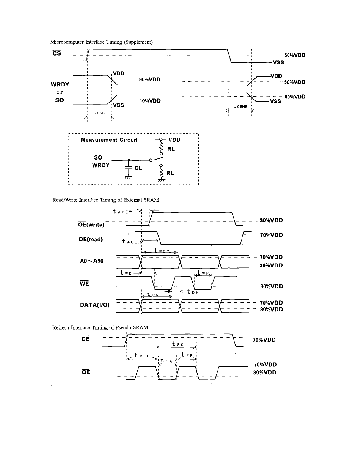
cancellation of SO,WRDY "Hi-z" (note2)
From CS"↑" to SO,WRDY"Hi-z" (note2)
From CS"↑" to DRDY"↓"
From SCLK"↓" to SO setup time (note2)
t
t
t
CSHS
CSDR
SOS
note 1 : Master clock cycle × 3
note 2 : See timing chart.
100
100
100
100
100
200
80
80
50
50
100
800
100
40
ns
ns
ns
ns
ns
ns
ns
ns
ns
ns
ns
ns
ns
ns
ns
0180-E-02 1997/12
- 17 -
Page 18
ASAHI KASEI [AK7712A-VT]
3)Read/Write Interface Timing of External RAM
(AVDD,DVDD,AVB,DVB=5.0V±5%, Ta=25°C, CL=20pF)
XTI(MHz)
18.432 16.934 12.288Parameter Symbol
Units
min max min max min max
Address delay time from OE "↑" (writing)
Address delay time from OE "↓" (reading)
Access time
Address set-up time
Data set time
Data hold time
Pulse width to write
t
t
t
t
t
t
t
AOEW
AOER
WCY
WD
DS
DH
WP
-15
105
10
80
10
60
1570-18
115
12
90
12
70
1880-20
170
15
135
15
90
20
110nsns
ns
ns
ns
ns
ns
4) Refresh Interface Timing of Pseudo SRAM(External RAM)
(AVDD,DVDD,AVB,DVB=5.0V±5%, Ta=25°C, CL=20pF)
XTI(MHz)
18.432 16.934 12.288Parameter Symbol
Units
min max min max min max
Auto refresh cycle
Pulse width of refresh command
Delay time of refresh command
Pre-charge time of refresh
t
FC
t
FAP
t
RFD
t
FP
145
80
100
35
162
90
110
40
210
135
160
60
ns
ns
ns
ns
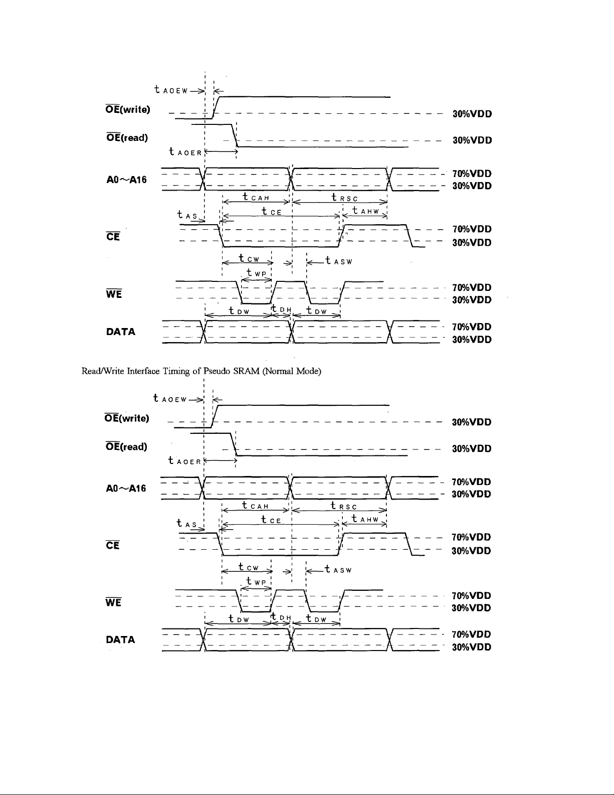
5) Read/Write Interface Timing of Pseudo SRAM(External RAM) (Static Column Mode)
(AVDD,DVDD,AVB,DVB=5.0V±5%, Ta=25°C, CL=20pF)
XTI(MHz)
18 .432 16.934 12.288Parameter Symbol
min max min max min max
Address delay time from OE "↑" (writing)
Address delay time from OE "↑" (reading)
Column address hold time
SC mode read/write cycle
Address setup time
Pulse width of chip enable
Column address hold time (after write)
Chip enable time
Column address setup time
Pulse width of write command
Data set time
Data hold time
t
t
t
t
t
t
t
t
t
t
t
t
AOEW
AOER
CAH
RSC
AS
CE
AHW
CW
ASW
WP
DW
DH
-15
110
80
10
180
10
95
10
35
50
10
1570-18
1880-20
120
90
12
200
12
105
12
40
60
12
170
135
15
280
15
140
15
60
90
15
Units
20
110nsns
ns
ns
ns
ns
ns
ns
ns
ns
ns
ns
0180-E-02 1997/12
- 18 -
Page 19
ASAHI KASEI [AK7712A-VT]
6) Read/write Interface Timing of Pseudo SRAM(External RAM) (normal mode)
(AVDD,DVDD,AVB,DVB=5.0V±5%, Ta=25°C, CL=20pF)
XTI(MHz)
18.432 16.934 12.288Parameter Symbol
Units
min max min max min max
Address delay time from OE "↑" (writing)
Address delay time from OE "↑" (reading)
Hold time of column address
Address setup time
Pulse width of chip enable
Pre-charge time of chip enable
Chip enable time
Pulse width of write command
Data set time
Data hold time
t
t
t
t
t
t
t
t
t
t
AOEW
AOER
CAH
AS
CE
P
CW
WP
DW
DH
-15
110
10
90
40
90
35
100
10
1570-18
120
12
100
50
100
40
110
12
1880-20
170
15
135
60
135
60
160
15
20
110nsns
ns
ns
ns
ns
ns
ns
ns
ns
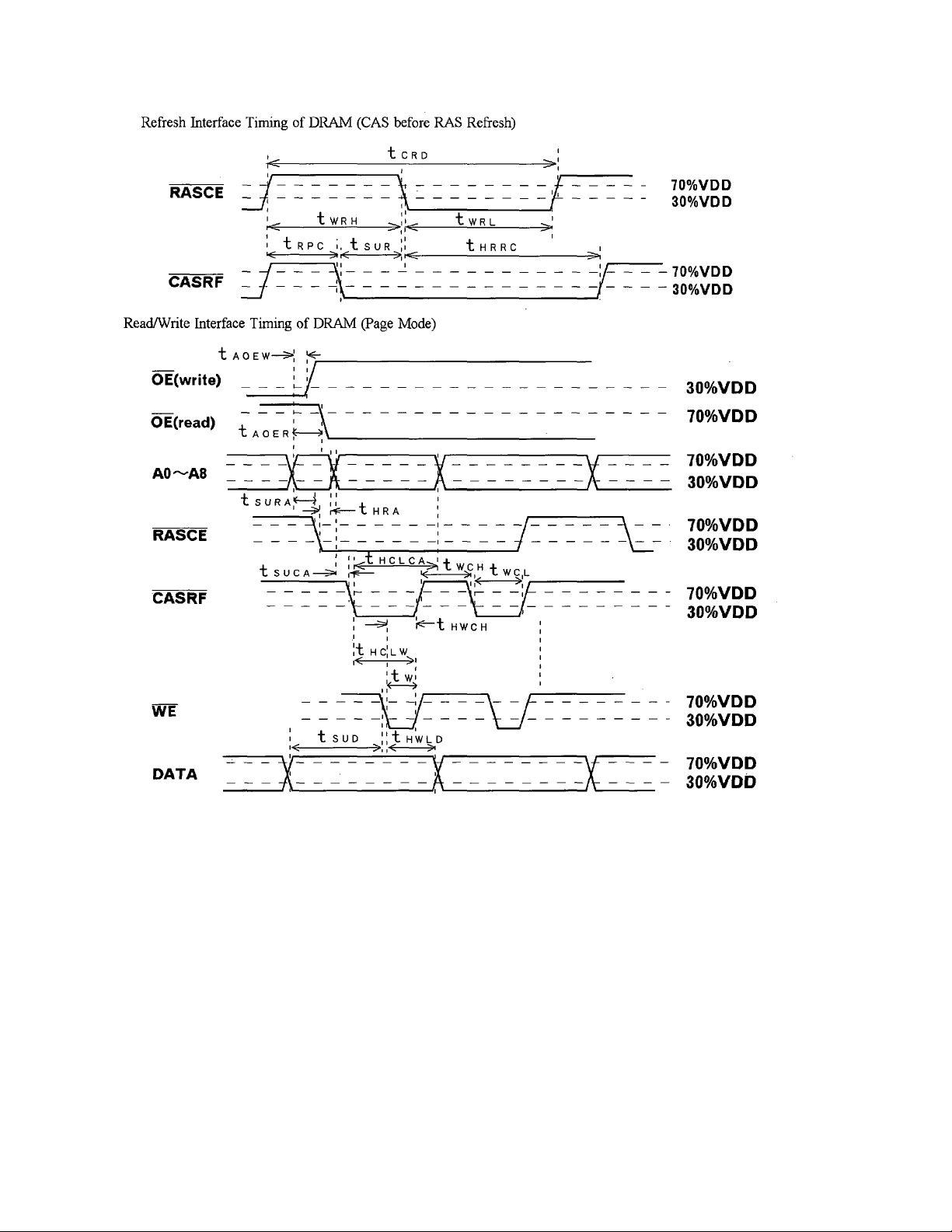
7) Refresh Interface Timing of DRAM(External RAM) (CAS before RAS Refresh)
(AVDD,DVDD,AVB,DVB=5.0V±5%, Ta=25°C, CL=20pF)
18.432 16.934 12.288Parameter Symbol
min max min max min max
Read cycle
Pulse width of RASCE"H"
Pulse width of RASCE"L"
•
RASCE Pre-charge
CASRF hold time
CASRF setup time at auto refresh
CASRF hold time at auto refresh
t
t
t
t
t
t
CRD
WRH
WRL
RPC
SUR
HRRC
240
105
105
80
10
200
8) Read/Write Interface Timing of DRAM(External RAM) (Page Mode)
(AVDD,DVDD,AVB,DVB=5.0V±5%, Ta=25°C, CL=20pF)
18.432 16.934 12.288Parameter Symbol
min max min max min max
Address delay time fromOE "↑" (write)
Address delay time fromOE "↓" (read)
RASCE preceded address setup time
RASCE followed address hold time
CASRF preceded address setup time
CASRF followed address hold time
CASRF hold time after write
Write hold time after CASRF
Write pulse width
Data setup time
Data hold time after write
Pulse width of CASRF"H"
Pulse width of CASRF"L"
t
AOEW
t
AOER
t
SURA
t
HRA
t
SUCA
t
HCLCA
t
HWCH
t
HCLW
t
W
t
SUD
t
HWLD
t
WCH
t
WCL
-15
10
12
10
45
40
55
40
0
60
22
54
1570-18
XTI(MHz)
260
120
120
90
12
220
XTI(MHz)
12
14
12
45
43
65
43
0
70
24
62
1880-20
360
170
170
130
15
320
15
18
15
60
60
90
60
100
32
90
0
Units
ns
ns
ns
ns
ns
ns
Units
20
110nsns
ns
ns
ns
ns
ns
ns
ns
ns
ns
ns
ns
0180-E-02 1997/12
- 19 -
Page 20
ASAHI KASEI [AK7712A-VT]
Timing Waveform
0180-E-02 1997/12
- 20 -
Page 21
ASAHI KASEI [AK7712A-VT]
0180-E-02 1997/12
- 21 -
Page 22
ASAHI KASEI [AK7712A-VT]
0180-E-02 1997/12
- 22 -
Page 23
ASAHI KASEI [AK7712A-VT]
Read/Write Interface Timing of Pseudo SRAM (Static Column Mode)
0180-E-02 1997/12
- 23 -
Page 24
ASAHI KASEI [AK7712A-VT]
0180-E-02 1997/12
- 24 -
Page 25
ASAHI KASEI [AK7712A-VT]
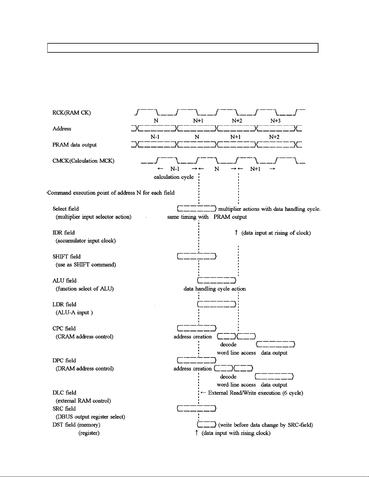
Function Manual
DSP unit : Execution Timing of Each Command
Each Blocks(PRAM,DRAM,CRAM,Calculation unit,etc.) actions on pipeline. On controlling of this pipeline, each
stages(command fetch, command decode and execution) are handled in parallel, The operations for each block is
executed by 32-bit holizontal code. Therefore each operations are executed equivalently in one machine cycle. The
following is the executing timing of each command.
0180-E-02 1997/12
- 25 -
Page 26
ASAHI KASEI [AK7712A-VT]
Calculation Function
1) Arithmetic System
0180-E-02 1997/12
- 26 -
Page 27
ASAHI KASEI [AK7712A-VT]
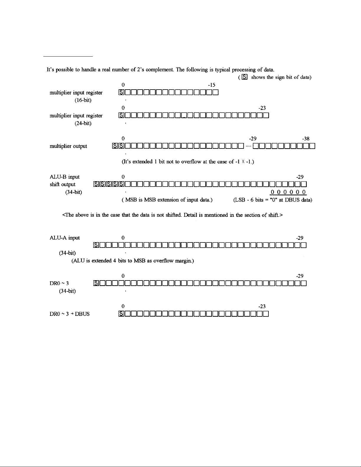
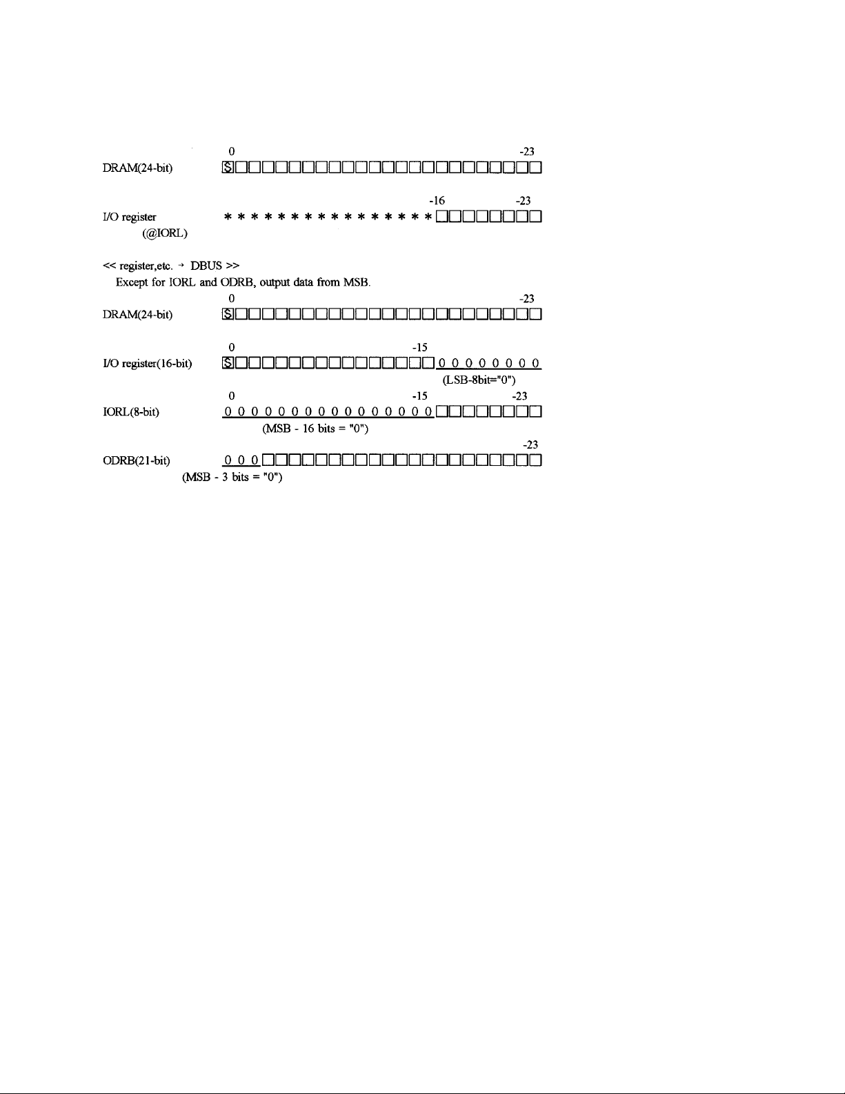
<< DBUS → register,etc. >>
Except for @IORL, take data from MSB.
0180-E-02 1997/12
- 27 -
Page 28

ASAHI KASEI [AK7712A-VT]
2) Multiplier
Multiplier outputs the 31-bit data for shift circuit as a result of fixed-point calculation(24-bit(data) × 16-bit(coefficient)
= 40-bit). 4 ways of multiplication can operate for the data as follows. The output data is extended from MSB for
reason that the data overflows at -1 × -1. The following combinations are possible for input.
16-bit Input 24-bit Input notes
Coefficient RAM
Coefficient RAM
DBUS
DBUS
Data RAM
DBUS
Data RAM
DBUS calculation of X
2
16-bit 24-bit
X Y
←Input Register
Partial Product
Carry Sum
←Partial Product Register
Final Adder
40-bit
Shifter
Multiplication actions always synchronous with CMCK, the product is output in 2 cycles.
0180-E-02 1997/12
- 28 -
Page 29

ASAHI KASEI [AK7712A-VT]
Together with shift function, each double-precision calculations of (24 × 31-bit), (45 × 31-bit) and (45 × 16-bit) are
available.
(24
,
(24 × 31-bit) calculation is done with Coefficient RAM data regulated as follows.
31-bit) Calculation
×
The obtained value X × YH should be added after shifting 16 bits to left compared with X × YL. But, as X × YL is the
data which is shifted 1bit to right, actually X × YH is added after shifting 15 bits to left.
<Example of Calculation Program (24 × 31-bit)>
,OP, , ,CPU,DU1,,, ;Read of Coefficient(MSB) and Data
,OP, , ,CPU, ,,, ;Read of Coefficient(LSB)
,OP,CR × DR , , , ,,,
,OP,CR × DR , , , ,,,
,OP, ,IDR0=SH0 << , , ,,,
,OP, ,IDR0=SHRF + LDR0 , , ,,, ;(X × YH) + 15-bit right-shifted (X × YL)
0180-E-02 1997/12
- 29 -
Page 30

ASAHI KASEI [AK7712A-VT]
This 34-bit data is shifted 15 bits to right and then is added to the upper data.
<Example of Calculation Program(45 × 31-bit)>
,OP, ,
,OP, ,
,OP,CR × DR ,
,OP,CR × DR ,
,OP,CR × DR ,IDR0=SDLF <<
,OP,CR × DR ,IDR1=SH0 <<
,OP,CR × DR ,IDR0=SHR6 + LDR0
,OP, ,IDR2=SHR6 <<
,OP, ,IDR0=SH0 + LDR0
,PP, ,IDR0=BHRF + LDR0
,OP, ,
,PP, ,IDR1=BDRF + LDR1
0180-E-02 1997/12
,CPU,DU1,, ,;Read of Coefficient(MSB) and Data(MSB)
, , ,, ,;
, ,DU1,, ,;YH × XH,Read of Data(LSB)
,CPU, ,, ,;YH × XH,Read of Coefficient(LSB)
, ,DD1,, ,;YH × XL(shifted 6bit to right)
, , ,, ,;YL × XL(shifted 21 to right)
, , ,, ,;YL × XH
, , ,, ,;
, , ,, ,;
, , ,,ODR2 ,;
, , ,, ,;ODRB: lower 24 bits data
, , ,,ODRB ,;DR1: upper 24 bits data
- 30 -
Page 31

ASAHI KASEI [AK7712A-VT]
(45
,
16-bit) Calculation
×
(45 × 16-bit) calculation is done with the data regulated as follows.
This 34-bit data is shifted 15 bits to right and then is added to upper data.
In this way, upper 24 bits and lower 21 bits are calculated.
<Example of Calculation Program(45 × 16-bit)>
,OP, ,
,OP, ,
,OP,CR × DR ,
,OP,CR × DR ,
,OP,CR × DR ,IDR0=SDLF <<
,OP, ,IDR1=SH0 <<
,OP, ,IDR0=SHR6 + LDR0
,OP, ,
,PP, ,IDR1=BDRF + LDR1
,CPU,DU1,, , ;Read of Coefficient(MSB), Data(MSB)
, , ,, , ;
,CPU, ,, , ;Y × XH,Read of Coefficient(LSB)
, , ,, , ;Y × XH
, , ,, , ;Y × XL(shifted 6bit to right)
, , ,, , ;
, , ,, , ;
, , ,, , ;ODRB: lower 24 bits data
, , ,,ODRB, ;DR1: upper 24 bits data
0180-E-02 1997/12
- 31 -
Page 32

ASAHI KASEI [AK7712A-VT]
3) Shift Calculation
The shift has two sources of multiplier output and DBUS. In the case of shortage of data length, MSB side is
extended the highest bit, LSB side is put in 0 to output 34-bits data. The shift commands which shift the data
0/1/2/3/4/6/8/15 bits to right/left, and the indirect shift command @SHR are prepared. On using the command (BH**)
which shift the DBUS data, you can use only CRAM and DRAM data for multiplication input at the same line. The
indirect shift command is carried out in 1 step, taking priority of shift field command. The Timing of shift command is
showed below.
0180-E-02 1997/12
- 32 -
Page 33

ASAHI KASEI [AK7712A-VT]
SDLF and BDRF take a peculiar action to calculate 45 × 31 and 45 × 16. The example program is shown on section
2) Multiplier. SDLF shifts the lower 15 bits of the product to 15 bits left, and calculates the 34 bits data, whose upper
13 bits and lower 6 bits are "0". The lower 6 bits of the product are set to "0" at next step.
BDRF shifts the 13 bits from upper extended data of DR0 to 15 bits right as input data, and extends this 19-bit data
from MSB for 15 bits upper, and then calculate 34-bit data, which is set the lower 6 bits to "0".
In this command, although not appoint DR register, DR0 data is chose and is added to upper data register.
(By hardware, the output of DR0 is directly connected to shift.)
• • •
•
A B C D E F
•
•
•
4-bit extension
↓shift to 15 bits right
• • • • • • • • • • • • • • •
• • • •
A B C D
• • • •
0 0 0 0 0 0
lower 6 bits ="0"
15-bit extension of MSB (extend from MSB of the extended 4 bits)
In addition to the direct shift command by the program mentioned above, the indirect shift, which execute with shift
number set to indirect shift command circuit, is prepared. The relation of shift and shift number is shown as following
colum. This circuit is connected with upper 5 bits of DBUS, and is set value by @SHR command, and then is carried
out in next step, taking priority of shift field command. Using this function and peak detection in P.44, the data can be
regulated. (ex. 163AFE(HEX) → 58EBF8(HEX)) The example of program is shown as follows. (assuming that DR0
is regulated.)
<Example of Data Regulating>
,OP,,
,OP,,
,PP,,IDR0=BH0 <<
,,,,ODR0 ,@PDR ;detecting size of DR0
,,,,PDR ,@SHR ;setting shift number with indirect shift
,,,,ODR0 , ;execution of indirect shift taking priority of BH0 after 1 step.
0180-E-02 1997/12
- 33 -
Page 34

ASAHI KASEI [AK7712A-VT]
Set value of shift number Shift Set value of shift number Shift
1 0 0 0 0 no shift 0 0 0 0 0 no shift
1 0 0 0 1 1 bit to right 0 0 0 0 1 1 bit to right
1 0 0 1 0 2 bits to right 0 0 0 1 0 2 bits to right
1 0 0 1 1 3 bits to right 0 0 0 1 1 3 bits to right
1 0 1 0 0 4 bits to right 0 0 1 0 0 4 bits to right
1 0 1 0 1 5 bits to right 0 0 1 0 1 5 bits to right
1 0 1 1 0 6 bits to right 0 0 1 1 0 6 bits to right
1 0 1 1 1 7 bits to right 0 0 1 1 1 7 bits to right
1 1 0 0 0 8 bits to right 0 1 0 0 0 8 bits to right
1 1 0 0 1 9 bits to right 0 1 0 0 1 9 bits to right
1 1 0 1 0 10 bits to right 0 1 0 1 0 10 bits to right
1 1 0 1 1 11 bits to right 0 1 0 1 1 11 bits to right
1 1 1 0 0 12 bits to right 0 1 1 0 0 12 bits to right
1 1 1 0 1 13 bits to right 0 1 1 0 1 13 bits to right
1 1 1 1 0 14 bits to right 0 1 1 1 0 14 bits to right
1 1 1 1 1 15 bits to right 0 1 1 1 1 15 bits to right
The function of shift is shown as follows.
<List of Shift Relational Command >
SH0: the product with no shift *BH0 : the DBUS data with no shift
SHR1: the product shifted 1 bit to right *BHR1: the DBUS data shifted 1 bit to right
SHR2: the product shifted 2 bits to right *BHR2: the DBUS data shifted 2 bits to right
SHR3: the product shifted 3 bits to right *BHR3: the DBUS data shifted 3 bits to right
SHR4: the product shifted 4 bits to right *BHR4: the DBUS data shifted 4 bits to right
SHR6: the product shifted 6 bits to right *BHR6: the DBUS data shifted 6 bits to right
SHR8: the product shifted 8 bits to right *BHR8 the DBUS data shifted 8 bits to right
SHRF: the product shifted 15 bits to right *BHRF the DBUS data shifted 15 bits to right
SHL1: the product shifted 1 bit to left *BHL1: the DBUS data shifted 1 bit to left
SHL2: the product shifted 2 bits to left *BHL2: the DBUS data shifted 2 bits to left
SHL3: the product shifted 3 bits to left *BHL3: the DBUS data shifted 3 bits to left
SHL4: the product shifted 4 bits to left *BHL4: the DBUS data shifted 4 bits to left
SHL6: the product shifted 6 bits to left *BHL6: the DBUS data shifted 6 bits to left
SHL8: the product shifted 8 bits to left *BHL8: the DBUS data shifted 8 bits to left
SHLF: the product shifted 15 bits to left *BHLF: the DBUS data shifted 15 bits to left
#SDLF: the product shifted 15 bits to left *#BDRF: the DBUS data shifted 15 bits to left
@SHR:Input the indirect shift value from DBUS(5 bits connection from MSB)
* : The use restriction is exist. (It can use when the input of multiplication is set to CRAM,DRAM.)
#: Special command used at double-precision calculation(45 × 31, 45 × 16).
0180-E-02 1997/12
- 34 -
Page 35

ASAHI KASEI [AK7712A-VT]
4) ALU
ALU can execute 34-bit arithmetic operation and 24-bit arithmetic•logical operation as follows.
<List of ALU Command>
* 34-bit arithmetic operation * 24-bit arithmetic•logical operation
+
<<
< 1
| |
/20, /18, /16
: A-B $
: A+B
: B through
: B through + 1
: the absolute value
: round
&
#
!
1 1+
: OR
: AND
: Exclusive-OR
: NOT
: A-1
: A+1
ALU outputs three flags mentioned below, holds the last flag's state at ALU-NOP.
* SGF: This flag shows MSB(+4 bits) of ALU. SGF flag shows "0" when the result is zero or positive,
and shows "1" when the result is negative.
* OVF: This flag shows the overflow(exceeding the 0-th bit) of operated result of ALU. When overflow is
occurred, it shows "1" else "0".
The data is output to DBUS as follows at overflow;
positive overflow: 7FFFFF(HEX) , negative overflow: 800000(HEX).
In addition, when the data exceed the overflow margin on the way of calculation, this flag is held on "1",
output the above data to DBUS.
* ZRF: This flag shows "1" when the result of 24-bit(0∼-23) calculation at ALU is "0".
The 20,18 and 16-bit rounding is prepared. 20-bit rounding execute the addition of "1" to -20th bit( if LSB = all "0"
then +0), and execute half-adjust. In the same way, 18-,16-bit rounding add "1" to -18th, -16th bit respectively. The
through +1 adds "1" to -24th bit, for the calculation data to be obtained as data rounded to 24-bit in advance, then
the execution step for rounding can be omitted. The location of addition point of "1" for 20-bit rounding is shown
below.
"<1" (B through +1) adds "1" to -25th bit of the input data. In the case that the calculated data is output on DBUS,
the data is rounded off to 24bits.
<Example program for 24-bit data output>
,OP,CR*DR, ,,,, , ;
,OP,CR*DR, ,,,, , ;
,OP,CR*DR,IDR0=SH0 <1 ,,,, , ;
,OP, ,IDR0=SH0 + LDR0 ,,,, , ;
,OP, ,IDR0=SH0 + LDR0 ,,,, , ;
,OP, , ,,,, , ;
,OP, , ,,,,ODR0, ;ODR0 is the rounded value of calculated data
0180-E-02 1997/12
- 35 -
Page 36

ASAHI KASEI [AK7712A-VT]
In each command of ALU, input data is processed as follows.
Command A input B input OF ZF SF OV ALU function
NOP
<<
<1
+
-
1-
1+
| |
/20
/18
/16
$
&
#
!
{: Flag is effective. ×: Don't care. RE: Reset of overflow register
About the timing of ALU, the input of B register actions always, but when ALU is NOP, the value of ACC and flag
are not changed. It becomes possible to output the result to DBUS 2 steps later .
all "0"
-24bits+1,all"0"
A
A
A
A
A
A
A,+1∼+4bits="0"
A,+1∼+4bits="0"
A,+1∼+4bits="0"
inversion
B
B
B
inversion+1
+4∼-23bits="1"
-24∼-29bits="0"
-23bits+1, all "0"
all "0"
-20bits+1, all"0"
-18bits+1, all"0"
-16bits+1, all"0"
B
B
B
all "0"
not change
{ { { {
{ { { {
{ { { {
{ { { {
RE
{ { {
RE
{ { {
{ { { {
{ { { {
{ { { {
{ { { {
{ × RE
×
{ × RE
×
{ × RE
×
{ × RE
×
+
+
+
+
+
+
positive: +
negative: invertion + 1
+
OR
AND
EXOR
NOT
0180-E-02 1997/12
- 36 -
Page 37

ASAHI KASEI [AK7712A-VT]
5) Division
The divider is equipped with a circuit independently. The condition and format of data are as follows.
Input data: A= dividient (16-bit)
: B= divisor (16-bit)
Output data: Q= quotient (16-bit)
Condition: 0<A<B ; A and B are positive, and Q is less than 1.
If input data is set in such order @DIVA,@DIVB on SRC field, the operation begins automatically, and the quotient is
obtained after 17 steps from @DIVB command, the result is held until the next direction of division. Then the data
output is available on and after 18th step. In this division, other calculation can be done. In such case, the order
@DIVA,@DIVB must be kept for operating division even if the same dividient or divisor data is used.
6) Pink noise generator circuitry
The single repatriated shift resistors [24, 21, 19, 18, 17, 16, 15, 14, 13, 10, 9, 5, 1]s are independently equipped in
this device apart from the arithmetic function block.
This circuitry renews the data at every sampling cycle and output data is connected to DBUS. As a result, the value
for 24bit can be asked at the sampling cycle when MRSG are pointed out in the DST field.
Besides, in case of use of pink noise generator circuitry, C5 should be set to 1 when control resistors are set.
0180-E-02 1997/12
- 37 -
Page 38

ASAHI KASEI [AK7712A-VT]
Accumulator(DR0
Accumulator is a 34-bit register to store the result of calculation at ALU. 4 registers of DR0~3 can be used. The
choice of accumulator to input data is done at IDR field. The data of accumulator is output to DBUS and the A-input
of ALU, and it is possible to select the different accumulators for LDR and SCR at the same time. The
accumulator0(DR0) can output to DBUS and moreover can output the lower 24 bits in 2 ways as follows. One of
those is the intact lower 24 bits, and the other is the 24 bits which is changed upper 3 bits of lower 24 bits to "0". The
upper 13 bits of DR0 is connected to shifter directly. In the case of output to DBUS, the data judged overflow is also
output the intact 24-bit data when TDR* command is used.
IDR0 : Input result of ALU to DR0 ODR0 : Output DR0 to DBUS with clip process
IDR1 : DR1 ODR1 : DR1
IDR2 : DR2 ODR2 : DR2
IDR3 : DR3 ODR3 : DR3
LDR0 : Output DR0 to the A input of ALU TDR0 : Output DR0 to DBUS without clip process
LDR1 : DR1 TDR1 : DR1
LDR2 : DR2 TDR2 : DR2
LDR3 : DR3 TDR3 : DR3
ODRB : Output the lower 24 bits of DR0 to DBUS
(upper 3 bits are "000")
ODRL : Output the lower 24 bits of DR0 to DBUS
∼∼∼∼
3)
<The List of Accumulator Command >
Temporary Register(TMP0
Temporary register is a 24-bit register to store the data of DBUS. The 8 registers of TMP0
choice of temporary register to input the data is done at DST field, and to output the data to DBUS is done at SRC
field. The data transport of inter- temporary register (ex: TMP0
TMP0 : Output TMP0 to DBUS @TMP0 : Input the data of DBUS to TMP0
TMP1 : Output TMP1 to DBUS @TMP1 : Input the data of DBUS to TMP1
TMP2 : Output TMP2 to DBUS @TMP2 : Input the data of DBUS to TMP2
TMP3 : Output TMP3 to DBUS @TMP3 : Input the data of DBUS to TMP3
TMP4 : Output TMP4 to DBUS @TMP4 : Input the data of DBUS to TMP4
TMP5 : Output TMP5 to DBUS @TMP5 : Input the data of DBUS to TMP5
TMP6 : Output TMP6 to DBUS @TMP6 : Input the data of DBUS to TMP6
TMP7 : Output TMP7 to DBUS @TMP7 : Input the data of DBUS to TMP7
∼∼∼∼
7)
TMP3) can be also done through DBUS.
→→→→
<The List of Temporary Register Command>
7 are available. The
∼∼∼∼
0180-E-02 1997/12
- 38 -
Page 39

ASAHI KASEI [AK7712A-VT]
Coefficient RAM(CRAM)
This is a RAM to store coefficient data for such as digital filter, and can be written the data through CBUS/DBUS. 3
ways are prepared for writing. The first way is to be loaded from such as microcomputer at reset of this LSI. The
second way is to write the 16 data written on microcomputer buffer at running state. The last way is writing from
DBUS, that is controlled by appointing at DST field. Output can be done to multiplier directly or to DBUS(lower 8 bits
are "0" ). The capacity of memory is 256 word × 16-bit. Two pointers are prepared. CP0 is reset to the
address"0(HEX)" and CP1 is reset to "80(HEX)" every sampling cycle, and appointment of pointer is set to CP0. The
address is able to increment(+1) and to decrement(-1). By load command, it is able to load the DBUS data directly
as pointer value. CPC command not only change the pointer but also does increment of the pointer change from.
For example, in the case of changing the pointer from CP0 to CP1, the change CP0 → CP1 and increment of
address of CP0 are done. The timing is shown below.
<List of CRAM Relational Command>
CPC: Pointer change(CP0 → CP1, CP0+1 ; CP1 → CP0, CP1+1)
CPU: Increment of address(+1)
CPD: Decrement of address(-1)
CRAM: Output the data to DBUS
@CP0: Load the data to CRAM-CP0 pointer (for address)
@CP1: Load the data to CRAM-CP1 pointer (for address)
@CRAM: Write DBUS data
It is explained below how those timing go in actual program.
,OP, ,,CPU,,, , ;be able to output to DBUS and multiplier(CR) 2 steps after
,OP, ,, ,,, , ;
,OP,CR*DR ,,CPU,,,CRAM, ;
,OP, ,, ,,,TMP0 , @CRAM ;write the data of TMP0 to the address made 1step before by CPU
,OP,CR*DR ,, ,,, , ;output the data written 1step before by @CRAM to CR and DBUS
,OP, ,,CPC,,, , ;
,OP, ,, ,,, , ;
,OP, ,, ,,, , ;output the data of pointer changed 2 steps before by CRC
,OP, ,, ,,, , ;operate with the changed pointer until next CPC is executed
0180-E-02 1997/12
- 39 -
Page 40

ASAHI KASEI [AK7712A-VT]
Data RAM(DRAM)
Data RAM is written through the DBUS, and is read on multiplier and DBUS directly. The capacity of memory is 128
word × 24 bit, and two memory pointers are prepared. The pointers of DP0 and DP1 are used after setting to
command register from outside before starting. The two method of addressing are prepared, the linear-addressing
method which starts with DP0:00H and DP1: 40H, and the ring-addressing method which increases start address
for every sampling cycle. When this ring-addressing is chosen, the address is added "1" for every sampling (start of
DP0 address:00→01→02→03→04……). The starting pointer appointment for every sampling cycle is chosen to
DP0. The address is able to increment(+1,+2,+3) and to decrement(-1,-2,-3). By load command, it is able to load the
DBUS data directly as pointer value. On using this load command, or loading DBUS data to pointer, the
value(loaded value + starting address at ring addressing method, loaded value at linear-addressing method) is
loaded to pointer. DPC command executes the change of pointer, at the same time the increment of changed
pointer. For example , when the pointer is changed from DP0 to DP1, not only the change of DP0→DP1 but also the
increment of address of DP0 are done. The timing of it is shown below.
<The List of DRAM Relational Command>
DPC: change pointer(DP0→DP1,DP0+1 ; DP1→DP0,DP1+1)
DU1: address+1 DD1: address-1
DU2: address+2 DD2: address-2
DU3: address+3 DD3: address-3
DRAM: output the data to DBUS(at the same time to selector of multiplier)
@DP0: load the DBUS data to DRAM-CP0 pointer
@DP1: load DBUS data to DRAM-CP1 pointer
@DRAM: write DBUS data
0180-E-02 1997/12
- 40 -
Page 41

ASAHI KASEI [AK7712A-VT]
It is explained below how the timing of previous page is go in actual program.
,OP, ,,,DU1,, , ;be able to output for DBUS and multiplier(DR) 2 steps after.
,OP, ,,, ,, , ;
,OP,CR*DR ,,,DU1,,DRAM, ;
,OP, ,,, ,,TMP0 ,@DRAM ;write the value of TMP0 to the address made 1 step before by DU1
,OP,CR*DR ,,, ,, , ;write the data written 1 step before by @DRAM to DR and DBUS.
,OP, ,,,DPC,, , ;
,OP, ,,, ,, , ;
,OP, ,,, ,, , ;output the data of pointer changed 2 steps before by DPC.
,OP, ,,, ,, , ;operation with changed pointer until the next DPC is executed
External RAM Control Unit
This unit controls the creation of write/read address, the RAM controlling signal and the receiving/transferring of 16bit delay data. 32k,128k×8-bit memories are used for SRAM and Pseudo SRAM, both or one of 64K and 256k ×4-bit
memories are used for DRAM. Addresses are received from OFRAM(40word × 16bit) data or inner calculation data,
i.e. DBUS data. The writing for external memory is done from small address number (00→01→02→03……) with ring
address method.
In the case of using OFRAM, the relative address is read from OFRAM in order of execution, and the real address is
calculated. So it needs to write the address data to OFRAM in order of execution. Each external
memory access requires 5 cycles of step DSP instruction at SRAM,P-SRAM(256k), and 6 c ycles at
DRAM,P-SRAM(1M). Writing of data to OFRAM is loaded from microcomputer or other unit at reset of
this LSI. At running state of LSI, if first address of changing data is appointed, 16 data can be automatically
changed at maximum in order of set address. When all data is changed, this command is automatically canceled . At
the case of using CRAM or internal calculation data(set the address by @DADR), after 2 cycles from @DADR
command execution, the execution of read/write command becomes be possible, on this time OFRAM does not
read next data. The maximum access number of times of memory are 76 for SRAM and Pseudo SRAM(256k) at
384fs, 51 at 256fs(DRAM, Pseudo SRAM(1M): 64/384fs, 42/256fs), and access time of usable memory is due to
input frequency of master clock(XTI) and sort of RAM for use, refer to switching features described in 18 - 19 page.
The timings are shown in Fig.1 for external RAM and SRAM, Fig.2, 3 for Pseudo 256k-SRAM at using auto-refresh
and static column mode read/write cycle, Fig.2 and 4 for Pseudo 1M-SRAM at using auto-refresh, read cycle and
write cycle (OE clock), Fig.5,6 for DRAM at using CAS before RAS refresh cycle and page mode read/write cycle.
<Address of Delay Data>
* Real address
= OFRAM data
+ sampling frequency after RUN
= calculation data + sampling frequency after RUN
* Relation of Write/Read address
appointed address: 2000H(Write)
↑
When the appointment of writing is not exist between these address,
Delay data of 2000H(Write) is read.
↓
appointed address: 1000H(Read)
Delay time of these above = (Write address-Read address) × ( 1/fs )
(2000H-1000H) × (1/44100) = 92.9msec
0180-E-02 1997/12
- 41 -
Page 42

ASAHI KASEI [AK7712A-VT]
0180-E-02 1997/12
- 42 -
Page 43

ASAHI KASEI [AK7712A-VT]
0180-E-02 1997/12
- 43 -
Page 44

ASAHI KASEI [AK7712A-VT]
The controlling of reading/writing are executed by micro code and have functions as follows.
<List of Control Command Related External RAM>
DLR : read RAM
DLW : write RAM
DRF : RAM refresh(needed at using DRAM or Pseudo SRAM)
IOR : output RAM data to upper 16 bits of DBUS
IORL : output RAM data to lower 8 bits of DBUS
@IOR : output upper 16 bits of DBUS data to data register for writing
@IORL : output lower 8 bits of DBUS data to data register for writing
(at external RAM-4bit, output the middle 8 bits to data register for writing)
@DADR : use upper 16bits of DBUS data for address
@OFP : upper 8bits of DBUS data to pointer
Peak Detection
Peak detection finds upper 16 bits of DBUS data as binary. The relation of input data and transformed value which
shows the size of data is as follows. If this value is used as indirect shift of @SHR command, data can be
normalized.
input data transformed value
01**************/10************** 00000
001*************/110************* 00001
0001************/1110************ 00010
00001***********/11110*********** 00011
000001**********/111110********** 00100
0000001*********/1111110********* 00101
00000001********/11111110******** 00110
000000001*******/111111110******* 00111
0000000001******/1111111110****** 01000
00000000001*****/11111111110***** 01001
000000000001****/111111111110**** 01010
0000000000001***/1111111111110*** 01011
00000000000001**/11111111111110** 01100
000000000000001*/111111111111110* 01101
0000000000000001/1111111111111110 01110
0000000000000000/1111111111111111 01111
0180-E-02 1997/12
- 44 -
Page 45

ASAHI KASEI [AK7712A-VT]
DBUS(Data BUS)
When output data to DBUS is less than 24 bits, the "0" data is supplemented from LSB side. Except @IORL
command, all input from DBUS is taken out the needed data length from MSB side. The @IORL inputs lower 8 bits
of DBUS data. When SRC field is NON or reset state, DBUS is set to "L".
Sequence Control Unit
It consists of 384word×32-bit PRAM(SRAM), micro program sequencer, 5-bit loop counter, 24-bit BUS interconnection, 8-bit return address register and 8-bit external condition register(IFCON). the writing data to PRAM,
which stores 32-bit horizontal macro command, is loaded at reset of DSP unit by such as microcomputer. By this 32bit horizontal micro command, the command is read at calculation command, and multiplication, addition,
subtraction and data transfer are operated in parallel. The micro program sequencer consists of 9-bit program
counter, 1 level stack register, pipeline instruction register and instruction decoder, LOOP, CAL, JMP, END,
conditional JMP, external conditional jump and load are executed. The stack is 9-bit and 1 level, and stores the
return address when subroutine call command is executed. By using this subroutine and LOOP, although program
capacity is 384 word, can be done 574 steps of operation at maximum when master clock is 576fs (sampling
frequency is 32kHz only). Using this feature, the loop command is convenience for reading/writing of external RAM.
As the stack is 1 level, it is not able to make call/loop command in the call/loop sentence. But conditional jump is
able to use in subroutine. When you make the program in that the jump is not return to the return address in call
sentence, AKM can not guarantee how does this DSP's action. This is same in loop command. At using that, it can
not return to the address stacked at call command. The BUS inter-connection between PBUS and DBUS realizes
that the 24-bit data is done the literal load to each register on DBUS by instruction. All sequence commands are 1
word commands(32-bit), and the time taken from the output of program counter to the end of command execution is
different in each command, but most of this is taken 2∼3 machine cycles. The timing of each instructions are shown
below.
Jump
,
The timing of jump is shown in the figure below. As the figure shows, 1 machine cycle of NOP is inserted
before jumping from the address of jump command to appointed address.
0180-E-02 1997/12
- 45 -
Page 46

ASAHI KASEI [AK7712A-VT]
Conditional Jump
,
The conditional jump is shown in the figure below. By this command, condition flag(SGF, OVF, ZRF of ALU) is
judged before jump, and if it is satisfied then the address of jump destination is set. Then 1 machine cycle of NOP is
inserted similar to jump. And if it is not satisfied then NOP is not inserted, and next address command is executed.
The list of conditional jump is shown below.
<List of Conditional Jump Command>
condition ALU(A-B)
JLE : SGF=1 or ZRF=1
JLS :
SGF=1
JGE : SGF=0
JGR : SGF=0 and ZRF=0
JZR :
ZRF=1
JNZ : ZRF=0
; A ≤ B
; A < B
; A ≥ B
; A > B
; A = B
; A ≠ B
JOV : OVF=1
JNO : OVF=0
0180-E-02 1997/12
- 46 -
Page 47

ASAHI KASEI [AK7712A-VT]
External Conditional Jump (JX)
,
The timing of external conditional jump is shown as follows. This command inputs the jump condition from outside of
LSI to 8-bit conditional jump register. When one of "1" of each bits of it and external conditional register is
coincident, the jump is executed. If it is satisfied, the address of jump destination is set. Then one machine cycle of
NOP is inserted similar to jump. And if the condition is not satisfied, NOP is not inserted, next address command is
executed.
The data is set to conditional jump register at rising edge of LRCK in motion or reset.
Subroutine Call (CL)
,
The timing of subroutine call is shown as follows. This command stacks next address before address of call
destination, NOP is inserted. The preparation for pushing the stacked address is done on return address, and stack
address is executed after return address. Then NOP is not inserted.
0180-E-02 1997/12
- 47 -
Page 48

ASAHI KASEI [AK7712A-VT]
Load Command (LD)
,
The timing of load command is shown in the figure below. This command loads the data to objective register through
the BUS inter-connection and DBUS.
End Command (ED)
,
The timing of end command is shown in the figure below.
This command inserts NOP until the rising edge of LRCK.
0180-E-02 1997/12
- 48 -
Page 49

ASAHI KASEI [AK7712A-VT]
Loop Command
,
The timing of loop command is shown in the figure below. This command operates the programs from next
command of the appointed sequence command for loop to the address appointed to return register loop
times(maximum 31(1Fh) times) over. NOP is not inserted at each the return.
0180-E-02 1997/12
- 49 -
Page 50

ASAHI KASEI [AK7712A-VT]
Input/Output Function
DSP unit of AK7712A has 4 channels of digital input port and 6 channels of digital output port. 2 channels of input
ports (SDIN2) can be connected to internal ADC, 2 channels of output ports (SDOUT2) can be connected to
internal DAC1. And another 2 channels of output ports(SDOUT3) can be connected to internal DAC2. The command
related to these above is as follows.
<List of ADC/DAC Command>
INL1(DINL): SDIN1-Lch→DBUS (connect SDIN1 )
INR1(DINR): SDIN1-Rch→DBUS (connect SDIN1 )
INL2(ADCL): SDIN2-Lch→DBUS (connect SDIN2 )
INR2(ADCR): SDIN2-Rch→DBUS (connect SDIN2 )
@OTL1(@DOTL): DBUS→SDOUT1-Lch register (connect SDOUT1 )
@OTR1(@DOTR): DBUS→SDOUT1-Rch register (connect SDOUT1 )
@OTL2(@DAL1): DBUS→SDOUT2-Lch register (connect SDOUT2 )
@OTR2(@DAR1): DBUS→SDOUT2-RCh register (connect SDOUT2 )
@OTL3(@DAL2): DBUS→SDOUT3-Lch register (connect SDOUT3 )
@OTR3(@DAR2): DBUS→SDOUT3-Rch register (connect SDOUT3 )
1) Digital Serial Input
The AK7712 provides 4 channels of digital serial input unit, and each interface format is as follows. This appointment
is done at control register.
SDIN1: MSB justified 24/16-bit, LSB justified 16-bit
SDIN2: MSB justified 20/16-bit
The data which is input from SDIN1(SDIN2) is distributed to each register DINL
•
DINR(ADCL•ADCR) at each rising
and falling edge of LRCK, and these data are output to DBUS 1 sampling cycle after. According to each data length,
the data is supplemented by "0" to lower bit, and is output to DBUS following SRC field.
2) Digital Serial Output
The AK7712 provides 6 channels of digital serial input unit, and each interface format is mentioned below. This
appointment is done at control register.
SDOUT1: MSB justified 24/16-bit, LSB justified 16-bit
SDOUT2: MSB justified 20/16-bit
Data is loaded to register by SRC field. MSB justified interface output the data taken 1 cycle before. At the rising
edge of LRCK both data of Lch and Rch are set to parallel/serial transformation register from upper bit of DBUS. In
the case above, it can not be guaranteed that the output command of last 4 steps of execution step in program are
output by the timing mentioned below.
0180-E-02 1997/12
- 50 -
Page 51

ASAHI KASEI [AK7712A-VT]
Serial Data Interface
The clocks which are needed are XTI, LRCK(fs) and BCLK( 32fs,48fs,64fs) at slave mode, and only XTI at master
mode. About the set-up for each format, please refer the section of control register. At master mode,the clock
needed is only XTI. Once input the XTI then LRCK(fs) and BCLK(64fs) are output. The input data is synchronized
with "↑" of BCLK. The output data is synchronized with "↓"of BCLK..
1.SDIN1, SDOUT1
1) Master Mode (64fs)
•
SDIN1 ( Input )
Control Register setting
16bit MSB justified 0 , 0
24bit MSB justified
16bit LSB justified 0 , 0
24bit LSB justified
C17, C16 C15, C14
0 , 0
0 , 0
0 , 0
0 , 1
1 , 0
1 , 1
Fig.7 SDIN1 Master Mode Input Format
•
SDOUT1 ( Output )
Control Register setting
16bit MSB justified 0 , 0
24bit MSB justified
16bit LSB justified 0 , 0
C17, C16 C13, C12
0 , 0
Fig.8 SDOUT1 Master Mode Output Format
0 , 0
0 , 1
1 , 0
0180-E-02 1997/12- 51 -
Page 52

ASAHI KASEI [AK7712A-VT]
2) Slave Mode
[64fs]
•
SDIN1 ( Input )
Control Register setting
16bit MSB justified 0 , 0
24bit MSB justified
16bit LSB justified 0 , 0
24bit LSB justified
C17, C16 C15, C14
0 , 0
0 , 0
0 , 0
0 , 1
1 , 0
1 , 1
•
SDOUT1 ( Output )
Control Register setting
16bit MSB justified 0 , 0
24bit MSB justified
16bit LSB justified 0 , 0
Fig.9 SDIN1 Slave Mode Input Format ( 64 fs )
C17, C16 C13, C12
0 , 0
0 , 0
Fig.10 SDOUT1 Slave Mode Output Format ( 64fs )
0 , 1
1 , 0
0180-E-02 1997/12- 52 -
Page 53

ASAHI KASEI [AK7712A-VT]
[48fs]
•
SDIN1 ( Input )
Control Register setting
16bit MSB justified 1 , 0
24bit MSB justified
16bit LSB justified 1 , 0
C17, C16 C15, C14
1 , 0
0 , 0
0 , 1
1 , 0
•
SDOUT1 ( Output )
Control Register setting
16bit MSB justified 1 , 0
24bit MSB justified
16bit LSB justified 1 , 0
Fig.11 SDIN1 Slave Mode Input Format ( 48 fs )
C17, C16 C13, C12
0 , 0
1 , 0
0 , 1
1 , 0
Fig.12 SDOUT1 Slave Mode Output Format ( 48fs )
0180-E-02 1997/12- 53 -
Page 54

ASAHI KASEI [AK7712A-VT]
[32fs]
•
SDIN1 ( Input )
Control Register setting
16bit MSB justified 0 , 1
C17, C16 C15, C14
0 , 0
Fig.13 SDIN1 Slave Mode Input Format ( 32 fs )
•
SDOUT1 ( Output )
Control Register setting
C17, C16 C13, C12
16bit MSB justified 0 , 1
Fig.14 SDOUT1 Slave Mode Output Format ( 32fs )
0 , 0
0180-E-02 1997/12- 54 -
Page 55

ASAHI KASEI [AK7712A-VT]
2.SDAD, SDIN2
1) Master Mode ( 64fs )
•
SDAD ( Output )
20bit MSB justified
Fig.15 SDAD Master Mode Output Format
•
SDIN2 ( Input )
Control Register setting
20bit MSB justified 0 , 0
16bit MSB justified
C17, C16 C11
0 , 0
0
1
Fig.16 SDIN2 Master Mode Input Format
0180-E-02 1997/12- 55 -
Page 56

ASAHI KASEI [AK7712A-VT]
2) Slave Mode
[64fs]
•
SDAD ( Output )
20bit MSB justified
Fig.17 SDAD Slave Mode Output Format ( 64fs )
•
SDIN2 ( Input )
Control Register setting
20bit MSB justified 0 , 0
16bit MSB justified
C17, C16 C11
0 , 0
0
1
Fig.18 SDIN2 Slave Mode Input Format ( 64fs )
0180-E-02 1997/12- 56 -
Page 57

ASAHI KASEI [AK7712A-VT]
[48fs]
•
SDAD ( Output )
20bit MSB justified
Fig.19 SDAD Slave Mode Output Format ( 48fs )
•
SDIN2 ( Input )
Control Register setting
20bit MSB justified 1 , 0
16bit MSB justified
C17, C16 C11
1 , 0
0
1
Fig.20 SDIN2 Slave Mode Input Format ( 48fs )
0180-E-02 1997/12- 57 -
Page 58

ASAHI KASEI [AK7712A-VT]
[32fs]
•
SDAD ( Output )
16bit MSB justified
Fig.21 SDAD Slave Mode Output Format ( 32fs )
•
SDIN2 ( Input )
Control Register setting
16bit MSB justified
C17, C16 C11
0 , 1
1
Fig.22 SDIN2 Slave Mode Input Format ( 32fs )
0810-E-02 1997/12- 58 -
Page 59

ASAHI KASEI [AK7712A-VT]
3.SDOUT2, SDDA
1) Master Mode ( 64fs )
•
SDOUT2 ( Output )
Control Register setting
20bit MSB justified 0 , 0
16bit MSB justified
C17, C16 C10
0 , 0
0
1
•
SDDA ( Input )
Control Register setting
20bit MSB justified
Fig.23 SDOUT2 Master Mode Output Format
C17, C16
0 , 0
Fig.24 SDDA Master Mode Input Format
0810-E-02 1997/12- 59 -
Page 60

ASAHI KASEI [AK7712A-VT]
2) Slave Mode ( 64fs )
[64fs]
•
SDOUT2 ( Output )
Control Register setting
20bit MSB justified 0 , 0
16bit MSB justified
C17, C16 C10
0 , 0
0
1
•
SDDA ( Input )
Control Register setting
20bit MSB justified
Fig.25 SDOUT2 Slave Mode Output Format ( 64fs )
C17, C16
0 , 0
Fig.26 SDDA Slave Mode Input Format ( 64fs )
0810-E-02 1997/12- 60 -
Page 61

ASAHI KASEI [AK7712A-VT]
[48fs]
•
SDOUT2 ( Output )
Control Register setting
20bit MSB justified 1 , 0
16bit MSB justified
C17, C16 C10
1 , 0
0
1
•
SDDA ( Input )
Control Register setting
20bit MSB justified
Fig.27 SDOUT2 Slave Mode Output Format ( 48fs )
C17, C16
1 , 0
Fig.28 SDDA Slave Mode Input Format ( 48fs )
0810-E-02 1997/12- 61 -
Page 62

ASAHI KASEI [AK7712A-VT]
[32fs]
•
SDOUT2 ( Output )
Control Register setting
16bit MSB justified
C17, C16 C10
0 , 1
1
Fig.29 SDOUT2 Slave Mode Output Format ( 32fs )
•
SDDA ( Input )
Control Register setting
20bit MSB justified
C17, C16
0 , 1
Fig.30 SDDA Slave Mode Input Format ( 32fs )
0810-E-02 1997/12- 62 -
Page 63

ASAHI KASEI [AK7712A-VT]
4.SDOUT3, SDDA2
1) Master Mode ( 64fs )
•
SDOUT3 ( Output )
Control Register setting
20bit MSB justified 0 , 0
C17, C16
•
SDDA2 ( Input )
Fig.31 SDOUT3 Master Mode Output Format
Control Register setting
20bit MSB justified
C17, C16
0 , 0
Fig.32 SDDA2 Master Mode Input Format
0810-E-02 1997/12- 63 -
Page 64

ASAHI KASEI [AK7712A-VT]
2) Slave Mode ( 64fs )
[64fs]
•
SDOUT3 ( Output )
Control Register setting
20bit MSB justified 0 , 0
C17, C16
Fig.33 SDOUT3 Slave Mode Output Format ( 64fs )
•
SDDA2 ( Input )
Control Register setting
20bit MSB justified
C17, C16
0 , 0
Fig.34 SDDA2 Slave Mode Input Format ( 64fs )
0810-E-02 1997/12- 64 -
Page 65

ASAHI KASEI [AK7712A-VT]
[48fs]
•
SDOUT3 ( Output )
Control Register setting
20bit MSB justified 1 , 0
C17, C16
Fig.35 SDOUT3 Slave Mode Output Format ( 48fs )
•
SDDA2 ( Input )
Control Register setting
20bit MSB justified
C17, C16
1 , 0
Fig.36 SDDA2 Slave Mode Input Format ( 48fs )
0810-E-02 1997/12- 65 -
Page 66

ASAHI KASEI [AK7712A-VT]
[32fs]
•
SDOUT3 ( Output )
Control Register setting
16bit MSB justified 0 , 1
•
SDDA2 ( Input )
Control Register setting
16bit MSB justified
C17, C16
Fig.37 SDOUT3 Slave Mode Output Format ( 32fs )
C17, C16
0 , 1
Fig.38 SDDA2 Slave Mode Input Format ( 32fs )
0810-E-02 1997/12- 66 -
Page 67

ASAHI KASEI [AK7712A-VT]
Microcomputer Interface
Microcomputer interface is operated with 7 control signals, which are SI(Serial data input), SO(Serial data output),
SCLK (Serial data input clock), WRDY(Write Ready), CS(Chip select), WRQ(Write Request) and DRDY(Data
Ready). All the data is done serial I/O with MSB first. The operating contents are transferred as 8-bit command data
shown below, and the appointed operations are executed.
<List of Command Code>
Write program RAM [RSPW](at reset) : code(1 1 0 0 0 0 0 0)
Write code for external conditional jump [JCON](at run,reset) : code(1 1 0 0 0 1 0 0)
Write coefficient RAM [RSCW](at reset) : code(1 0 1 0 0 0 0 0)
Write coefficient RAM [RNCW](at run) : code(1 0 1 0 0 1 0 0)
Write offset RAM [RSOW](at reset) : code(1 0 0 1 0 0 0 0)
Write offset RAM [RNOW](at run) : code(1 0 0 1 0 1 0 0)
Prepare to write CRAM/OFFRAM [RNBW](at run) : code(1 0 0 0 1 0 0 0)
Write control register [CONW](at reset) : code(0 0 0 0 0 1 1 0)
1) Writing Program RAM
The writing to program RAM is executed with 7bytes/set at reset. If all the data is transferred, WRDY pin becomes
"L", and if the writing to PRAM is finished, it becomes "H" and next data becomes be able to be input. In case of
writing data with the continuos address, input the data directly(command code and address are not needed). If it's
discontinuous, set WRQ pin "H"→"L", and input in the order of command code, address and data.
<Data Transfer Procedure>
1
command code (1 1 0 0 0 0 0 0)
{
2
address(Upper) (0 0 0 0 0 0 0 A8)
{
2
address(Lower) (A7 • • • • • • A0)
{
3
data (D31 • • • • • • D24)
{
4
data (D23 • • • • • • D16)
{
5
data (D15 • • • • • • D8)
{
6
data (D7 • • • • • • D0)
{
2) Writing Coefficient RAM
The writing coefficient RAM(at reset) is executed with 4bytes/set data. If all the data is transferred, WRDY pin
becomes "L", and if the writing to CRAM is finished, it becomes "H" and next data becomes be able to be input. In
case of writing data with the continuos address, input the data directly. If it's discontinuous, set WRQ pin "H"→"L",
and input in the order of command code, address and data.
<Data Transfer Procedure>
1
command code (1 0 1 0 0 0 0 0)
{
2
address (A7 • • • • • • A0)
{
3
data (D15 • • • • • • D8)
{
4
data (D7 • • • • • • D0)
{
0180-E-02 1997/12- 67 -
Page 68

ASAHI KASEI [AK7712A-VT]
3) Writing Offset RAM
The writing to program RAM is executed with 4bytes/set at reset. If all the data is transferred, WRDY pin becomes
"L", and if the writing to OFFRAM is finished, it becomes "H" and next data becomes be able to be input.
In case of writing data with the continuos address, input the data directly. If it's discontinuous, set WRQ pin "H"→"L",
and input in the order of command code, address and data.
<Data Transfer Procedure>
1
command code (1 0 0 1 0 0 0 0)
{
2
address (0 A6 • • • • • • A0)
{
3
data (D15 • • • • • • D8)
{
4
data (D7 • • • • • • D0)
{
4) Preparation of Rewriting Coefficient•Offset RAM(RUN State) and Rewriting
This is used to rewrite the coefficient•offset RAM when program is running. After input of command code, the data,
which is wanted to rewrite with the continuos address, can be able to input up to 16. Secondary, if the write
command code and first address for rewrite are input then contents of RAM is rewritten every appointment of the
rewritten RAM address. For example, when 5 data are rewritten by address"10" of coefficient RAM, it's executed as
follows.
coefficient RAM execution address 7 8 9 10 11 13 16 11 12 13 14 15
↓ ↓ ↓ ↓ ↓
rewrite execution position { { ↑ { { {
address"13" is not rewritten until address"12" is rewritten.
<Data Transfer Procedure>
* Rewrite preparation
* Rewrite
:OFRAM (1 0 0 1 0 1 0 0)
1
command code (1 0 0 0 1 0 0 0)
{
2
data (D15 • • • • • • D8)
{
3
data (D7 • • • • • • D0)
{
1
command code:CRAM (1 0 1 0 0 1 0 0)
{
2
first address (A7 • • • • • • A0)
{
0180-E-02 1997/12- 68 -
Page 69

ASAHI KASEI [AK7712A-VT]
5) Writing Code for External Conditional Jump
The writing code for external conditional jump is executed with 2byte/set. It is able to input at both of reset run, and
the input data is set to register at rising of LRCK. When all the data is transferred, WRDY becomes "L", and if the
writing is finished, it becomes "H". The external conditional code is 8-bit, and if any one or more of bits of this code is
coincident with "1" of each code of IFCON field, the jump command is executed. When the data is written at reset
state, it can be executed only after all the data transferred or before cancel. Please set WRQ to "H" after 150nsec or
more after rising of LRCK after cancellation of reset at write on reset state.
< Data Transfer Procedure>
1
command code (1 1 0 0 0 1 0 0)
{
2
code data (D7 • • • • • D0)
{
6) Writing Control Register
The writing control register(at reset) is executed with 4bytes/set. When all the data is transferred, WRDY becomes
"H", and if the writing is finished, it becomes "H".
<Data Transfer Procedure>
1
command code (0 0 0 0 0 1 1 0)
{
2
control data (C23 • • • • • • C16)
{
3
controla data (C15 • • • • • • C8)
{
4
control data (C7 • • • • • • C0)
{
The register, which is controlling the action mode of this LSI, is consists of 24 bits.
The function of each bit is shown in Table 1 as follows.
0180-E-02 1997/12- 69 -
Page 70

ASAHI KASEI [AK7712A-VT]
[ Table 1 ]
Bit name Function
C23 External RAM data length selection 1: 4-bit, 0: 8-bit(default value)
External RAM selection (C22,C21,C20) = (0,0,0): SRAM (default value) C22
C21
C20
(0,1,0): Pseudo SRAM(static column mode)
(0,1,1): Pseudo SRAM(normal mode)
(1,0,0): DRAM 256K
(1,0,1): DRAM 1M(use as 512K)
C19 Data reset function selection after reset 1: not use, 0: use(default value)
Addressing method selection of DRAM 0: Ring addressing (default value) C18
1: Linear addressing
C17
C16
BCLK selection (C17,C16) = (0,0): 64fs(default value)
Effective only slave mode
(0,1): 32fs
(1,0): 48fs
SDIN1 interface selection (C15,C14) = (0,0): MSB justified 16-bit 32/48/64fs C15
C14
(0,1): MSB justified 24-bit 48/64fs
(1,0): LSB justified 16-bit 48/64fs
(1,1): LSB justified 24-bit 64fs
SDOUT1 interface selection (C13,C12) = (0,0): MSB justified 16-bit 32/48/64fs C13
C12
(0,1): MSB justified 24-bit 48/64fs
(1,0): LSB justified 16-bit 48/64fs
(0,0): (default value)
SDIN2 interface selection 0: MSB justified 20-bit 48/64fs C11
1: MSB justified 16-bit 32/48/64fs
0: (default value)
SDOUT2 interface selection 0: MSB justified 20-bit 48/64fs C10
1: MSB justified 16-bit 32/48/64fs
0: (default value)
Reserve/ Test (C9,C8) = (0,0): (default value) note 1) C9
C8
C7 Reserve/ Test 0: (defaul value) note 1)
C6 ADC HPF selection 1: not use, 0: use(default value)
C5 Pink Noise Generation 0: (default value) 1: use
C4 Reserve/ Test 0: (default value) note 1)
C3
C2
Master clock selection (C3,C2) = (0,1): (default value)
XTI DSP fs Max clock
(0,0): 384fs 384fs 48/44.1/32kHz 18.432MHz
(0,1): 256 256 48/44.1/32 12.288MHz
(1,0): 512
(1,1): 576
512
576
32
32
16.384MHz
18.432MHz
C1 Reserve/ Test 0: (default value) note 1)
C0 Reserve/ Test 0: (default value) note 1)
* Other codes except for this table are reserved. Do not use these reserved codes.
note 1) Do not change the reserve/ test as it may be used for test. It may become the cause of irregular action.
0180-E-02 1997/12- 70 -
Page 71

ASAHI KASEI [AK7712A-VT]
7) Timing with Microcomputer
In case of transferring data from microcomputer, the command data can be input on condition that the WRQ is set to
"H", the command register is reset and WRQ is set to "L". CS must be set to "L" in case of receiving/ transferring
data from/to this LSI. If CS is set to "H", then SO and WRDY become "Hi-z" state and can not receive/transform
data. The timing of data load at reset(RST ="L", PD ="Hi") is shown in Fig.38 and 39. If the transferring data is
finished then WRDY signal becomes "L", and if down load is finished then it return to "H".
The motion transferring next data is suppressed in that period(WRDY= "L"). Since the period has short length about
2 cycles of master clock, if SCLK is slow enough then monitoring of WRDY is not needed.
Fig.38 Input of Continuos Address Data to PRAM,CRAM and OFRAM
Fig.39 Input of Discontinuos Address Data to PRAM,CRAM and OFRAM
0180-E-02 1997/12- 71 -
Page 72

ASAHI KASEI [AK7712A-VT]
In case of changing the data of CRAM and OFRAM data at RUN state, execute preparation of writing data at run
state(in this case, address is unnecessary and RST is "H") by writing to buffer memory similar to Fig.11. Secondary,
set WRQ to "L" and if input of command code and address is finished then set WRQ to "H". If the preparation for
rewrite is finished inside, WRDY signal becomes "L", and rewrite command is executed from rising of LRCK. And if
rewriting is finished, WRDY becomes to "H". These timing is shown in Fig.41.
•
•
• •
•
•
Fig.41 Data Rewrite Timing at Run State
0180-E-02 1997/12- 72 -
Page 73

ASAHI KASEI [AK7712A-VT]
The external conditional jump can be written at reset/run state. These timing are shown in Fig.42 and 43. At reset
state, the "L"→"H" in WRQ must be executed after 3MCK from "L"→"H" in RST. But, at run state, "L"→"H" in WRQ
can be executed at once after transferring jump condition. WRDY signal becomes "H"→"L" after transferring jump
condition, and 2 cycles after setting RST/WRQ to "H", becomes "L"→"H" at rising edge of LRCK. As similar to
above, data transferring is suppressed in the period of WRDY="L".
•
•
• •
•
•
Fig.42 Write Timing External Conditional Jump at Reset
•
•
•
•
••
Fig.43 Write Timing of External Conditional Jump at Run time
0180-E-02 1997/12- 73 -
Page 74

ASAHI KASEI [AK7712A-VT]
SO can output the data on DBUS of this LSI. By appointing @MICR at DST field, the data is set, and DRDY
becomes to "H", and the data is put synchronizing with falling edge of SCLK. If once CS is changed to "H", DRDY
becomes to "L", and wait the next command. If once DRDY becomes to "H", the data of first @MICR command after
DRDY="H" is held and other command is not received while CS is held "L".In case of output from SO, set WRQ to
"H", and CS to "L".
Fig.44 Output Timing of SO
* Attentions concerning of control signal for micro computer interface
Control signal for micro computer interface(CS, RST, WRQ should be allowed to change when SCLK is in "H" state.
* SO output is maximum 24bit data. After obtaining the indispensable number of data(less than 24), the subsequent
data can be possible to output when CS is in "H" state.
High-pass Filter
AK7712A has digital high-pass filter(HPF) for DC offset cancel. HPF is active when control register C6 is "0". The
cut-off frequency of HPF is about 1Hz(fs=48kHz). If C6 is set to "1" then HPF becomes unavailable. In that case,
AK7712A has DC offset of a few millivolts.
Zero detection function
In the case that "0" of both channels of input data repeats 8192 times, DZF becomes "H". After that, if input data
becomes not "0" then DZF becomes "L" at once.
0180-E-02 1997/12- 74 -
Page 75

ASAHI KASEI [AK7712A-VT]
System Clock
The system clock of AK7712A is XTI at master
mode. And these are XTI, LRCK(fs) and BCLK at
slave mode. In case of using slave mode, XTI and
LRCK must be synchronized but those phases do not
need to be muched.
Internal Clock Circuit
Master clock can be obtained by quartz oscillator
connected between XTI pin and XTO pin, or by
openning XTO pin and inputting the external
clock to XTI pin.
The frequencies of each clocks needed for standard
audio rate is shown in the table below.
Example of Quartz Oscillator Connection
LRCK (fs)
(kHz)
44.1
48.0
(fs) (MHz)
256 8.1920
384 12.288032.0
512 16.3840
256 11.2896
384 16.9344
256 12.2880
384 18.4320
XTI
0180-E-02 1997/12- 75 -
Page 76

ASAHI KASEI [AK7712A-VT]
Notes on Use
1) In the case that external clock is not supplied at run state
At run state(PD="H"), do not stop each external clock. XTI at master mode, and XTI,BCLK and LRCK at slave mode
are needed. If these clocks are not supplied, the circuit is overloaded and the action becomes abnormal since the
dynamic logic is used inside.
2) In the case that system clock frequency is changed
At slave mode, the inside timing must be synchronized with LRCK supplied from outside. This synchronization is
done by reset inside master counter. This reset is done only one time at LRCK"↑" after RST "↑". After that, digital
filter operates only with inside master clock, writes data to output register. In the case that synchronism breaks down
by changing each system clock frequency, the output data may become anomaly for overlap of write timing to output
register and read timing by LRCK. So, change clock with RST "L"(PDAD,PDDA="L"), and reset both built-in
ADC,DAC. But, the phase shift between LRCK and inside timing is out of the range from 1/16 to -1/16 of input
sampling cycle(1/fs), the adjustment of phase of inside timing is done synchronized with LRCK"↑"(same as reset
state).
0180-E-02 1997/12- 76 -
Page 77

ASAHI KASEI [AK7712A-VT]
Reset Control
1) System Reset
During power-up, please reset by setting both PD and RST pin "L" to "H". The reset is cancelled at XTI "↑". Then,
the inside timing becomes to synchronize with LRCK"↑", and the inside LRCK becomes to action since 4LRCK
after, and DSP unit becomes to action.
2) Powerdown-Reset control
The reset is controlled with 2 pins of system reset(RST)and power down(PD). It is also able to control the state of
ADC/DAC by using PDAD/PDDA pins in support.
• The setting of "PD:L, RST:L" makes all the circuit reset and MOS resistance of quartz oscillator OFF. In this
state, by stopping XTI, BCLK and LRCK, power down state is realized(the leak is checked with this state at test).
At "PD:L, RST:L", since MOS resistance of quartz oscillator is also off, output from CLKO and XTO can not be
guaranteed.
"PD:L, RST:L" is used at power on, or at setting to power down state.
• If "PD:H, RST:L" is set, each register of DSP unit is reset(control register is not reset), and PRAM, DRAM and
OFRAM become write enable state. In that case, both of AD unit and DA unit become reset( power down)
state(when PDAD and PDDA are "L").
• The reset( power down) state is cancelled at first "↑" of XTI after setting RST to "H". In that case, DAC output is
done after 2Ts cycles, but ADC takes 516Ts cycles for initialize, then output data becomes "0". (Ts = 1/fs)
By PDAD/PDDA, the control of reset state(power down) for AD/DA unit can be separated to the control of reset
for DSP unit. Usually both of PDAD and PDDA are used with "L". But in the case that DSP is reset and
PRAM,DRAM and OFRAM are rewritten, not to make ADC and DAC power down state, please set PDAD and
PDDA to "H" after power on.
PD "L" "H" "H" "H" "H" "H"
RST "L" "L" "L" "L" "L" "H"
PDAD - "L" "L" "H" "H" PDDA - "L" "H" "L" "H" -
AD PD Õ Õ RUN RUN RUN
DA PD Õ RUN Õ RUN RUN
(-: Don't care, PD: power down, RUN: run state, Õ: can not run)
The format is shown in the table .
In the case of writing data to control
register, set PDAD and PDDA to "L".
To make the change of PDAD and
PDDA, set RST to "L".
0180-E-02 1997/12- 77 -
Page 78

ASAHI KASEI [AK7712A-VT]
3)Action of DSP Unit, at Reset
This LSI has two kinds of reset; "reset(RST)" and "power down(PD)". If RST is set to "L"(PD ="H"), each register is
reset, and PRAM,CRAM and OFRAM become write enable state. If RST is set to "H"(PD="H"), the reset is
cancelled, and the external RAM clear("0" data write) and the write data"0" to internal DRAM are executed from the
rising edge of LRCK. this period takes 2260*1/fs [sec](fs: sampling frequency). In periods of reset and of write
"0"data to DRAM, input/output data is operates as "0". In these periods, DZF is kept "H". These period take
51.3msec at 44.1kHz(384fs). To be disable this function, set control register C19 to "1".This timing is shown in
Fig.45.
Fig.45 Timing at Reset and after Cancellation of Reset
If both of RST and PD are set to "L", this LSI becomes power down state, so the control register is also reset to
default state. After cancellation, it actions same above. To change the control register or program, set PD to "H", load
data, set RST to "H".
Fig.46 Timing at Power Down and after Cancellation of Reset
0180-E-02 1997/12- 78 -
Page 79

ASAHI KASEI [AK7712A-VT]
System Design
Connection :
0180-E-02 1997/12- 79 -
Page 80

ASAHI KASEI [AK7712A-VT]
The connection to external RAM is as follows.
0180-E-02 1997/12- 80 -
Page 81

ASAHI KASEI [AK7712A-VT]
<Pseudo SRAM>
0180-E-02 1997/12- 81 -
Page 82

ASAHI KASEI [AK7712A-VT]
Periphery Circuit
1. Ground and Power Supply
In AK7712A, to keep the coupling of digital noise in minimum, AVDD and DVDD are done the decoupling
independently.AVDD,AVB and DVB are supplied with analog power supply of system. AVB and DVB are connected
each other by IC-substrate, and have a resistance of several ohms. If AVDD, AVB, DVB and DVDD are supplied by
another power supply, AVDD,AVB and DVB must be powered at the same time as DVDD ,or AVDD,AVB,DVB must
be powered at first. In the general way, separate both of power supply and ground between analog and digital, and
connect near power supply on PC board. The decoupling capacitor, especially ceramic capacitor of small capacity
must be connected near AK7712A.
Caution: Keep AVDD,A VB,DVB ≥ DVDD-0.3V, or the over current causes latch-up and this IC may fall into destruction.
2. Standard Voltage
The difference of input voltage between VRADH pin and VRADL pin decide the full-scale of analog input, and the
difference of voltage between VRDAH pin and VRDAL pin decide the full-scale of analog output. Usually connect
VRADH with AVDD1, and VRDAH with AVDD2, and connect the ceramic capacitor of 0.1uF between AVSS1 and
µ
AVSS2. VCOM is used as the common voltage of analog signal. Connect electrolytic capacitor about 10
F and the
ceramic capacitor of 0.1uF in parallel between this pin and AVSS to remove high-frequency noise. Especially, the
ceramic capacitor must be connected to the pin as near as possible. Do not get current from VCOM pin. Digital
signal, especially the clock must be parted as far as possible from VRADH,VRADL,VRDAH,VRDAL and VCOM pin
to avoid the coupling to AK7712A.
3. Analog Input
Analog input signal is input to modulator from differential input pin of each channel. The input voltage is differential of
AIN+ and AIN- (∆V
AIN
=(AIN+)-(AIN-)), and the input range is
± FS=± (VRADH-VRADL) × 0.4 .
When VRADH=5V and VRADL=0V, the input range is ±2.0V. The code of output code format is 2's complement. The
output code against the input voltage is shown in Table 2.
input voltage
output code (sexadecimal digit)
16-bit 20-bit
>(+FS-1.5LSB) 7FFF 3FFFF
-0.5LSB
0000
FFFF
00000
7FFFF
<(-FS+0.5LSB) 8000 80000
Table 2. input voltage vs. output code
At fs=48kHz, AK7712A does sampling the analog input with 3.072MHz. The digital filter removes noise between
30kHz and 3.042MHz. But near 3.072MHz, noise is not removed. Since almost all audio signal does not have
noise near 3.072MHz, so the noise can be reduced enough by simple RC filter.
The standard voltage of A/D conversion is input to VRADH pin and VRADL pin. Usually VRADH is connected with
AVDD1 and VRADL is connected with AVSS1. To remove high-frequency noise, connect 10uF electrolytic capacitor
and 0.1uF ceramic capacitor in parallel between VRADH pin and VRADL pin.
Since the analog power supply voltage of AK7712A is set to +5V, do not input the voltage more than (AVDD1)+0.3V
or the voltage less than (AVSS1)-0.3V or the current more than 10mA to analog input pin(AINL,AINR). The over
current causes destruction of inner protective circuit, moreover latch-up, and the IC falls into destruction.
0180-E-02 1997/12- 82 -
Page 83

ASAHI KASEI [AK7712A-VT]
Accordingly, in the case that power supply voltage of periphery analog circuit is ±15V, then it is needed to protect
the analog input pin from the signal which is more than maximum absolute rating.
Fig.47 Example of Input Buffer Circuit(Differential Input)
Fig.48 Example of Input Buffer Circuit(Single-end Input)
It is also available to input analog signal to AK7712A with single-end. In that case, input the analog signal(in case of
usingthe inner standard voltage, the full-scale is 4.0Vp-p) to AIN-input, and input the bias to AIN+input. But, at using
single-end input type, 2nd harmonic distortion is pretty big, then the features of S/N+D will be worse than at using
differential input (Fig.48).
4. Analog Output
The analog output is single-end type, the output range is 2.9Vpp(typ) and centered on VCOM voltage. outband
noise(shaping noise), which is generated by built-in ∆Σ modulator, is reduced by built-in switched capacitor
filter(SCF) and continuous filter(CTF). Accordingly, it is not needed to add external filter in usual use. The input code
format is 2's complement, and the output is positive full-scale at 7FFFH(@16-bit), the negative full-scale at
8000H(@16-bit) and ideally VCOM voltage at 0000H(@16-bit).
0180-E-02 1997/12- 83 -
Page 84

ASAHI KASEI [AK7712A-VT]
As analog output of this LSI has DC offset of several mV, cut the DC component by capacitor in usual use. Fig.49 is
a example of external circuit that makes the output double. In this example, output is reversed.
Fig.49 Example of External Circuit(Gain; 2)
5. Connection with Digital Circuit
To minimize the noise caused by digital circuit, connect CMOS logic to digital output. The conformable logic families
are 4000B, 74HC, 74AC, 74ACT and 74HCT.
0180-E-02 1997/12- 84 -
Page 85

ASAHI KASEI [AK7712A-VT]
Package
100pin LQFP (Unit: mm)
Material & Lead finish
Package: Epoxy
Lead-frame: Copper
Lead-finish: Soldering plate
0180-E-02 1997/12- 85 -
Page 86

ASAHI KASEI [AK7712A-VT]
Marking
XXXXAAA Data Code Identifier
XXXX: Assembly Date (number)
AAA: Lot Number (alphabet)
0180-E-02 1997/12- 86 -
Page 87

IMPORTANT NOTICE
z These products and their specifications are subject to change without notice. Before
considering any use or application, consult the Asahi Kasei Microsystems Co., Ltd. (AKM)
sales office or authorized distributor concerning their current status.
z AKM assumes no liability for infringement of any patent, intellectual property, or other
right in the application or use of any information contained herein.
z Any export of these products, or devices or systems containing them, may require an
export license or other official approval under the l aw and regulations o f the country of
export pertaining to customs and tariffs, currency exchange, or strategic materials.
z AKM products are n either intended n or authorized for us e as critical c omponents in any
safety, life support, or other hazard related device or system, and AKM assumes no
responsibility relating to any such use, except with the express written consent of the
Representative Director of AKM. As used here:
(a) A hazard related device or system is one designed or intended for life support or
maintenance of safety or for applications in medicine, aerospace, nuclear ener gy, or
other fields, in which its failure to function or perf orm may reasonably be expected to
result in loss of life or in significant injury or damage to person or property.
(b) A critical component is one whose fail ure to function or perfor m may reasonably be
expected to result, whether directly or indirectly, in the loss of the safety or
effectiveness of the device or system containing it, and which must therefore meet
very high standards of performance and reliability.
z It is the responsibility of the buyer or distributor of an AKM product who distributes,
disposes of, or otherwise places the product with a third party to notify that party in
advance of the above content and conditions, and the buyer or distributor agrees to
assume any and all r esponsibility and liability for and ho ld AKM harmless from any and
all claims arising from the use of said product in the absence of such notification.
 Loading...