

Page 1
ASAHI KASEI
[AK61584]
Features
- Provides Dual Analog PCM Line Interface
for short-haul,T1 and E1 applications
- Jitter Tolerance: Compliant with AT&T62411
TR-NWT-000499 Category
- Transmitter Pulse Shape: Compliant with
AT&T62411,CB119, TR-NWT-000499,
ITU-T G.703
- Jitter Transfer: AT&T62411, ITU-T G.736
- Operating mode fully software configurable.
No external quartz crystal
- Support of JTAG boundary scan
Serial Port
Hardware mode
IPOL (Note) CS INT SCLK
RLOOP2ATTEN0ATTEN1RLOOP1LLOOP1LLOOP2TAOS1TAOS2
I
,II ITU-T G.823
is required.
SDO SDI SPOL
AK61584
Dual Low Power T1/E1 Line Interface
- Low Power Consumption
- 3.3Volt operation
- Small Plastic Package 64pin LQFP(
1.4mm
)
10*10*
General Description
The AK61584 is a universal line interface for T1/E1 applications, designed for high-volume cards where low power,
high density and universal operation is required. One board
design can support all T1/E1 modes.
The AK61584 is a low-power CMOS device available
in 3.3 Volt.
CON01 CON02 CO N11 CON12 CON 21 CON22 COD ER1 CODER2 CLKE
TDATA1)TPOS 1
(
RDATA1)RPOS1
(
TDATA2)TPO S2
(
RDATA2)RPOS2
(
TCLK1
(AIS1)TNEG1
RCLK1
(BPV1)RNEG 1
TCLK2
(AIS2)TNEG2
RCLK2
(BPV2)RNEG2
ENCODER DECORDER
ENCODER DECORDER
JTAG
4
CONTROL
REMOTE LOOPBACK
JITTER
ATTENUATOR
REMOTE LOOPBACK
JITTER
ATTENUATOR
CLOCK GENERATOR
2
REFCLK 1XCLK TV+ TGND RV+ RGND DV+ DGND AV+ AG ND BGREF PD1 PD2 LOS1 LOS2
2
LOCAL LOOPBACK1
TAOS
LOS&
AIS
DETECT
LOCAL LOOPBACK1
TAOS
LOS&
AIS
DETECT
22
PULSE
SHAPING
CIRCUITRY
CLOCK&
DATA
RECOVERY
PULSE
SHAPING
CIRCUITRY
CLOCK&
DATA
RECOVERY
3
DRIVER
DRIVER
CONTROL
Note) In host mode, this pin must be tied to GND.
LOCAL LOOPBACK2
TTIP1
TRING1
RTIP1
RRING1
LOC AL LOO PBACK2
TTIP2
TRING2
RTIP2
RRING2
RESET
MODE
Preliminary Product Information
This document contains information for a new product. AKM
reserves the right to modify this product without notice.
0185-E-00 98/04
-1-
Page 2

ASAHI KASEI
Table of Contents
Block Diagram................................................................................ 1
Specifications
General Description
Pin Description..............................................................................32
[AK61584]
Absolute Maximum Ratings............................................ 3
Recommended Operating Conditions .............................. 3
Digital Characteristics..................................................... 4
Analog Specifications
Receiver.............................................................. 4
Jitter Attenuator.................................................. 4
Transmitter ......................................................... 5
Switching Characteristics
T1 Clock/Data .................................................... 6
E1 Clock/Data .................................................... 6
Serial Port........................................................... 8
JTAG.................................................................. 9
Overview........................................................................10
Operating Options..........................................................11
Overview of Applications...............................................12
Transmitter.....................................................................13
Receiver.........................................................................15
Jitter Attenuator..............................................................16
Coder Mode...................................................................17
Reference Clock.............................................................17
Loopbacks......................................................................17
Power Down ..................................................................17
Reset..............................................................................18
Power-On Reset.............................................................18
Control...........................................................................18
Registers ........................................................................21
Host-Mode Register Access ...........................................23
Arbitrary Waveform Generation.....................................24
Power Supply.................................................................24
JTAG Boundary Scan.....................................................24
0185-E-00 98/04
-2-
Page 3
ASAHI KASEI
[AK61584]
ABSOLUTE MAXIMUM RATINGS
Parameter Symbol Min Max Units
DC Supply(TV+1,TV+2,RV+1,RV+2,AV+,DV+)(Note 1) - 6.0 V
Input Voltage Any Pin Vin RGND-0.3 (RV+)+0.3 V
Input Current Any Pin (Note 2) Iin -10 10 mA
Ambient Operating Temperature TA -40 85
Storage Temperature Tstg -65 150
o
C
o
C
WARNING:Operations at or beyond these limits may result in permanent damage to the device.
Normal operation is not guaranteed at these extremes.
Notes: 1. Referenced to RGND1,RGND2,TGND1,TGND2,AGND,DGND at 0V.
2. Transient currents of up to 100 mA will not cause SCR latch-up.
RECOMMENDED OPERATING CONDITIONS
Parameter Symbol Min Typ Max Units
DC Supply(TV+1,TV+2,RV+1,RV+2,AV+,DV+)
(Note 3) 3.135 3.3 3.465 V
Ambient Operating Temperature TA -40 25 85
Power Consumption T1 (Notes 4 and 5)
(Each Channel) T1
(Notes 4 and 6)
E1,75ohm (Notes 4 and 5)
E1,120ohm (Notes 4 and 5)
REFCLK Frequency T1 1XCLK=1 1.544-
T1 1XCLK=0 12.352E1 1XCLK=1 2.048E1 1XCLK=0 16.384-
PC -
100ppm
100ppm
100ppm
100ppm
292
-
-
-
167
180
170
380
220
210
200
1.544 1.544+
100ppm
12.352 12.352+
100ppm
2.048 2.048+
100ppm
16.384 16.384+
100ppm
Notes: 3. TV+1,TV+2,AV+,DV+,RV+1,RV+2 should be connected together.TGND1,TGND2,RGND1,
RGND2,DGND1,DGND2,DGND3 should be connected together.
4. Power consumption while driving line load over operating temperature range. lncludes IC and load.
Digital input levels are within 10% of the supply rails and digital outputs are driving a 50 pF
capacitive load.
5. Assumes 100% ones density and maximum line length at 3.465V.
6. Assumes 50% ones density and 300ft. line length at 3.3V.
o
MW
MW
MW
MW
MHz
MHz
MHz
MHz
C
0185-E-00 98/04
-3-
Page 4
ASAHI KASEI
[AK61584]
DIGITAL CHARACTERISTICS (TA=-40 to 85
o
C;power supply pins within +/-5% of nominal)
Parameter Symbol Min Typ Max Units
High-Level input Voltage (Note 7) VIH (DV+)-0.5 - - V
Low-Level input Voltage (Note 7) VIL - - 0.5 V
High-Level Output Voltage (Note 8)
VOH (DV+)-0.3 - - V
IOUT=-40uA
Low-Level Output Voltage (Note 8)
VOL - - 0.4 V
IOUT=1.6mA
Input Leakage Current
- - +/-10 uA
(Digital pins except INT, J_TMS, and J_TDI)
Notes: 7. Digital inputs are designed for CMOS logic levels.
8. Digital outputs are TTL compatible and drive CMOS levels into a CMOS load.
ANALOG SPECIFICATIONS (TA=-40 to 85
o
C;power supply pins within +/-5% of nominal)
Parameter Min Typ Max Units
Receiver
Input Impedance between RTIP/RRING - 20k - ohm
Sensitivity Below DSX-1(0 dB=2.4V) -13.6 - - DB
Loss of signal threshold, Short Haul
T1
E1
Data Decision Threshold T1,DSX-1 (Note 9)
(Note 10)
E1 (Note 11)
(Note 12)
60
55
45
40
-
-
0.23
0.15
65
-
50
-
70
75
55
60
-
-
V
V0p
0p
% of
Peak
Allowable Consecutive Zeros before LOS 160 175 190 bits
Receiver Input Jitter 10 Hz and below (Note 13)
Tolerance(DSX-1,E1) 2 kHz
10 kHz-100 kHz
300
6.0
0.4
-
-
-
-
-
-
UIpp
UIpp
UIpp
Jitter Attenuator
Jitter Attenuation Curve Corner Frequency (Note 14 and 15)
T1
E1
-
-
4
5.5
-
-
Hz
Hz
Attenuation at 10 kHz Jitter frequency (Note 14 and 15) - 60 - dB
Attenuator Input Jitter Tolerance (Note 14)
28 43 - UIpp
(Before Onset of FIFO Overflow or Underflow Protection)
Notes: 9. For input amplitude of 1.2Vpk to 4.14Vpk
10. For input amplitude of 0.5Vpk to 1.2Vpk, and 4.14Vpk to 5.0Vpk
11. For input amplitude of 1.07Vpk to 4.14Vpk
12. For input amplitude of 4.14Vpk to 5.0Vpk
13. Jitter tolerance increases at lower frequencies. See Figure 11.
14. Not production tested. parameters guaranteed by design and characterization.
15. Attenuation measured with sinusoidal input jitter equal to 3/4 of measured jitter tolerance.
Circuit attenuates jitter at 20 dB/decade above the corner frequency. See Figure 16. Output jitter
can increase significantly when more than 28 UI’s are input to the attenuator. See discussion in
jitter Attenuator section.
0185-E-00 98/04
-4-
Page 5

ASAHI KASEI
[AK61584]
ANALOG SPECIFICATIONS (TA=-40 to 85
o
C;power supply pins within +/-5% of nominal)
Parameter Min Typ Max Units
Transmitter
AMI Output Pulse Amplitudes (Note 16)
E1,75ohm (Note 17)
E1,120ohm (Note 18)
T1,DSX-1 (Note 19)
2.14
2.7
2.4
2.37
3.0
3.0
2.6
3.3
3.6
V
0p
V0p
V0p
Recommended Transmitter Output Load (Note 16)
T1,
E1,75ohm
E1,120ohm
-
-
-
25
43
68.9
-
-
-
ohm
ohm
ohm
Jitter Added
by the Transmitter 8kHz – 40kHz
10Hz – 40kHz
Broad Band (Note 20)
Power in 2 kHz band about 772 kHz (Notes 14 and 21)
-
-
-
0.013
0.016
0.027
-
-
-
UI
pp
UIpp
UIpp
12.6 15 17.9 dBm
(DSX-1 only)
Power in 2 kHz band about 1.544 MHz (Notes 14 and 21)
-29 -38 - dB
(referenced to power in 2 kHz band at 772 kHz) (DSX-1 only)
Positive to Negative Pulse Imbalance (Notes 14 and 21)
T1,DSX-1
E1,amplitude at center of pulse interval
E1,width at 50% of nominal amplitude
-5
-5
-
0.2
-
-
0.5
+5
+5
dB
%
%
Transmitter Return Loss (Notes 14, 21, and 22)
51 kHz - 102 kHz
102 kHz - 2.048 MHz
2.048 MHz - 3.072 MHz
8
14
10
-
-
-
-
-
-
dB
dB
dB
E1 Short Circuit Current (Note 23) - - 50 mArms
E1 and DSX-1 Output Pulse Rise/Fall Times (Note 24) - 25 - ns
E1 Pulse Width (at 50% of peak amplitude) - 244 - ns
E1 Pulse Amplitude E1, 75ohm
for a space
E1,120ohm
-0.237
-0.3
-
-
0.237
0.3
0p
V
V0p
Notes: 16. Using a transformer that meets the specifications in Table 2.
17. Measured across 75ohm at the output of the transmit transformer for CON2/1/0=0/0/0.
18. Measured across 120ohm at the output of the transmit transformer for CON2/1/0=0/0/1.
19. Measured at the DSX-1 Cross-Connect for line length settings CON2/1/0=0/1/0, 0/1/1,
1/0/0, 1/0/1, and 1/1/0 after the length of #22 ABAM cable specified in Table 1.
20. Input signal to TCLK is jitter free.
21. Typical performance with a 0.47 uF capacitor in series with primary of transmitter output transformer.
22. Return loss = 20 log
Z
23. Transformer secondaries shorted with 0.5ohm resistor.
24. At transformer secondary. From 10% to 90% of amplitude.
=cable impedance.
0
ABS ((z1+z0)/(z1-z0)) where z1 = impedance of the transmitter, and
10
0185-E-00 98/04
-5-
Page 6
ASAHI KASEI
[AK61584]
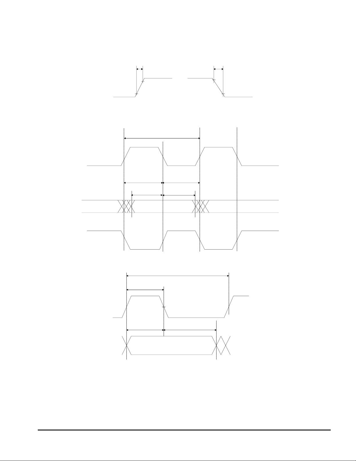
SWITCHING CHARACTERISTICS-T1 CLOCK/DATA (TA = -40 to 85
pins within +/-5% of nominal; Inputs: Logic 0=0V, logic 1=DV+)(See Figures 1,2, and 3)
o
C;power supply
Parameter Symbol Min Typ Max Units
TCLK Frequency (Note 25) ftclk - 1.544 - MHz
TCLK Duty Cycle tpwh2/tpw2 30 50 70 %
RCLK Duty Cycle (Note 26) tpwh1/tpw1 45 50 55 %
Rise Time All Digital Outputs (Note 27) tr --65ns
Fall Time All Digital Outputs (Note 27) tr --65ns
TPOS/TNEG to TCLK Falling Setup Time tsu2 25 - - ns
TCLK Falling to TPOS/TNEG Hold Time th2 25 - - ns
RPOS/RNEG to RCLK Rising Setup Time tsu1 - 274 - ns
RCLK Rising to RPOS/RNEG Hold Time th1 - 274 - ns
Notes: 25. Max value of 8.192 MHz describes the maximum burst rate of a gapped input clock(TCLK).
For the gapped clock to be tolerated by the AK61584, the jitter attenuator must be switched to
transmit path of the line interface. The maximum gap size is defined in the Analog Specification table.
26. RCLK duty cycle may be outside the spec limits when jitter attenuator is in the receive path,
and when the jitter attenuator is employing the overflow/underflow protection mechanism.
27. At max load of 50pF .
SWITCHING CHARACTERISTICS-E1 CLOCK/DATA (TA = -40 to 85
pins within +/-5% of nominal; Inputs: Logic 0=0V, Logic 1=DV+)(See Figures 1, 2, and 3)
o
C;power supply
Parameter Symbol Min Typ Max Units
TCLK Frequency (Note 25) ftclk - 2.048 - MHz
TCLK Duty Cycle tpwh2/tpw2 30 50 70 %
RCLK Duty Cycle (Note 26) tpwh1/tpw1 45 50 55 %
Rise Time All Digital Outputs (Note 27) tr --65ns
Fall Time All Digital Outputs (Note 27) tr --65ns
TOPS/TNEG to TCLK Falling Setup Time tsu2 25 - - ns
TCLK Falling to TOPS/TNEG Hold Time th2 25 - - ns
RPOS/RNEG to RCLK Rising Setup Time tsu1 - 194 - ns
RCLK Rising to RPOS/RNEG Hold Time th1 - 194 - ns
0185-E-00 98/04
-6-
Page 7
ASAHI KASEI
[AK61584]
Any Digital O ut put
Figure 1. Signal Rise and Fall Characteristics
RCLK
(for CLK E =hig h)
RPOS
RNEG
(RDATA)
RCLK
(for CLK E =lo w )
tr
90%
10%
tpwl1
tsu 1
tf
90%
10%
tpw1
tpw h 1
th1
Figure 2. Recoverd Clock and Data Switching Characteristics
tpw 2
tpwh2
TCLK
tsu 2
th2
TPOS/TNEG
(TDATA)
Figure 3. Transmit Clock and Data Switching Characteristics
0185-E-00 98/04
-7-
Page 8
ASAHI KASEI
[AK61584]
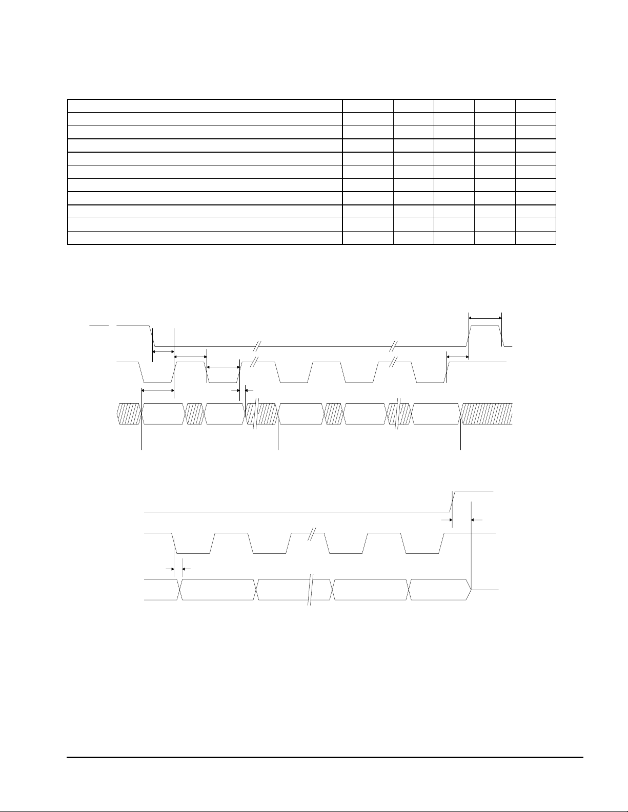
SWITCHING CHARACTERISTICS -SERIAL PORT (TA = -40 to 85
DV+,TV+,RV+ = nominal +/-0.3V; Inputs: Logic 0 = 0V, Logic 1 = RV+)
o
C;
Parameter Symbol Min Typ Max Units
SDI to SCLK Setup Time tdc 25 - - ns
SCLK to SDI Hold Time tcdh 25 - - ns
SCLK Low Time tcl 50 - - ns
SCLK High Time tcl 50 - - ns
SCLK Rise and Fall Time tr,tf --15ns
CS to SCLK Setup Time tcc 20 - - ns
SCLK to CS Hold Time (Note 28) tcch 20 - - ns
CS Inactive Time tcwh 100 - - ns
SCLK to SDO Valid (Note 29) tcdv --50ns
CS to SDO High Z tcdz -50-ns
Notes: 28. If SPOL=0, then CS should return high no sooner than 20ns after the 16‘th falling edge of SCLK
during a serial port read.
29. Output load capacitance = 50 pF.
tcwh
CS
tcc
tch
tcl
tcch
SCLK
SDI
SCLK
SPOL= 0
CS
SDO
tdc
LSB
CONTROL BYTE
tcdh
LSB
MSB
DATA BYTE
Figure 4. Serial Port Write Timing Diagram
tcdv
Figure 5. Serial Port Read Timing Diagram
tcdz
High-Z
0185-E-00 98/04
-8-
Page 9
ASAHI KASEI
[AK61584]
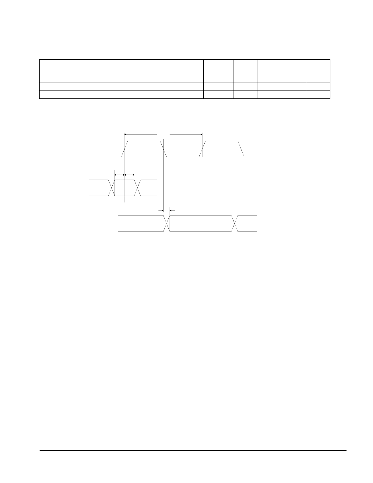
SWITCHING CHARACTERISTICS -JTAG (TA = -40 to 85
TV+,RV+ = nominal +/-0.3V; Inputs: Logic 0 = 0V, Logic 1 =RV+)
o
C;
Parameter Symbol Min Typ Max Units
Cycle Time tcyc 200 - - ns
J_TMS/J_TDI to J_TCK rising setup time tsu 50 - - ns
J_CLK rising to J_TMS/J_TDI hold time th 50 - - ns
J_TCLK falling to J_TDO valid tdv --50ns
tcyc
J_TCK
tsu
th
J_TM S
J_TDI
tdv
J_TD O
Figure 6. JTAG Swithing Characteristics
0185-E-00 98/04
-9-
Page 10
ASAHI KASEI
[AK61584]
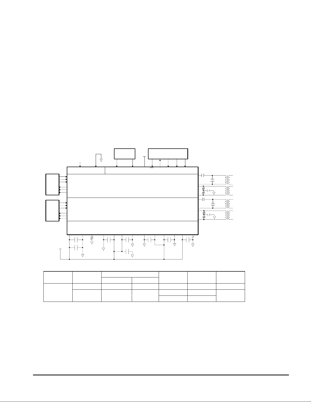
OVERVIEW
The AK61584 is a universal line interface for
T1/E1 applications, designed for high-volume cards
where low power, high density and universal operation is required. One board design
can support
all T1/E1 short-haul modes. The T1 and E1 modes
can be selected entirely via software.
As shown in Figure 1, the AK61584 provides all
the functions needed for a line interface
including a
line driver, a receiver and jitter attenuator.
The line driver generates waveforms compatible
with E1 (ITU-T G.703),T1 short haul (DSX-1).
Framer
Framer
12.352MHz
REFCLK
TCLK1
TPOS1
TNEG1
RCLK1
RPOS1
RNEG1
TCLK2
TPOS 2
TNEG2
RCLK2
RPOS2
RNEG2
Clock
Clock
1XCLK
Control
IPOL RESET
Channel 1
Channel 2
Power Supply
VCC
MODE INTCSSCLK
Control
The driver internally matches the impedance of the
load, providing excellent return loss. The benefit of
the internal impedance matching is a 50 percent
reduction in power consumption compared to implementing return loss with external resistors. With
external
resistors a driver has to drive the equiva-
lent of two line loads.
The receiver contains clock and data recovery circuits.
The jitter attenuator meets AT&T 62411 requirements without the use of an external quartz crystal.
The attenuator does require an external reference
clock.
Micro Controller
serial port
SDI
SDO
TRING1
RRING1
TRING2
RRING2
TTIP1
RTIP1
TTIP2
RTIP2
R1
R2
R3
R4
0.47uF
470pF
(E1)
0.47uF
0.47uF
470pF
(E1)
0.47uF
T1
transmit
1:N
T2
receive
1:N
T3
transmit
1:N
T4
receive
1:N
Vcc
AV+
AGND
+
0.1uF
1uF
BGREF
R3
5kohm
TGND2 TV+2 TV+1
0.1uF
0.1uF
+
22uF
TGND1
RGND2
0.1uF
RV+2
RV+1
RGND1
0.1uF
DV+
DGND
3
0.01uF
Vcc Data Rate REFCLK Frequency MHz Cable R1-R4 Transformers
Volts MHz 1XCLK=1 1XCLK=0 ohm ohm T1-T4
1.544 1.544 12.352 100 12.5 1:2
3.3 2.048 2.048 16.384 75 21.5 1:1.32
120 34.4
Figure 7 - Typical Connection Diagram
( Host Mode)
0185-E-00 98/04
-10-
Page 11

ASAHI KASEI
[AK61584]
OPERATING OPTIONS
The following are the major operating options which
are supported by the AK61584:
Control
Control of the AK61584 is via either host mode (seri-
al port) or hardware mode (individual control lines).
Hardware mode offers significantly fewer programmability options than the host mode.
T1/E1
The AK61584 supports T1 short-haul (DSX-1), and
E1 operation. The configuration pins (CON <0:2>)
and register bits control transmitted pulse shapes,
transmitter source impedance, and receiver slicing
level. Both channels must be operated at the same
rate (both T1 or both E1).
The pulse shapes are fully pre-defined by circuitry in
the AK61584, and are fully compliant with appropriate standards when used with our application guidelines in standard installations.
T1/E1 framing device. Alternatively, a coder mode
can be selected. In coder mode, an internal
B8ZS/AMI/HDB3 coder can be used on those systems which don't need T1/E1
framers (typically
high-speed multiplexers). In host mode, the choice of
transmit encoder is independent of the choice of receiver decoder.
Reference Clock
The AK61584 requires a T1 or E1 reference clock.
This clock can be either a 1-X clock (i.e.,1.544 MHz
or 2.048MHz). or can be a 8-X clock (i.e., 12.352
MHz or 16.384 MHz). In systems which want software selection of data rate, the
1-X clock option is
typically chosen, and the reference clock is tied to the
transmit clock. In systems with a jittered transmit
clock, an external oscillator should drive the reference
clock input, and a 8-X rate can be used to minimize
the physical size of the oscillator. In either case, any
jitter present on the reference clock will not be filtered
by the jitter attenuator, and the reference clock should
have 100 ppm or better frequency accuracy.
Power Down
The transmitter impedance changes with the line
length options in order to match the impedance of the
load (75-ohm for E1 coax, 100-ohm for T1, 120- ohm
for E1 Shielded twisted pair).
receiver slicing level is set at 65% for DSX-1
The
short-haul, and at 50% for all other applications.
Line Codes
The AK61584 supports a transparent mode where
the line code is encoded and decode by an external
Either one of the two line interfaces may be independently powered down.
Jitter Attenuator
The jitter attenuator may be placed in the receiver
path, the transmit path or bypassed entirely.
0185-E-00
98/04
-11-
Page 12
ASAHI KASEI
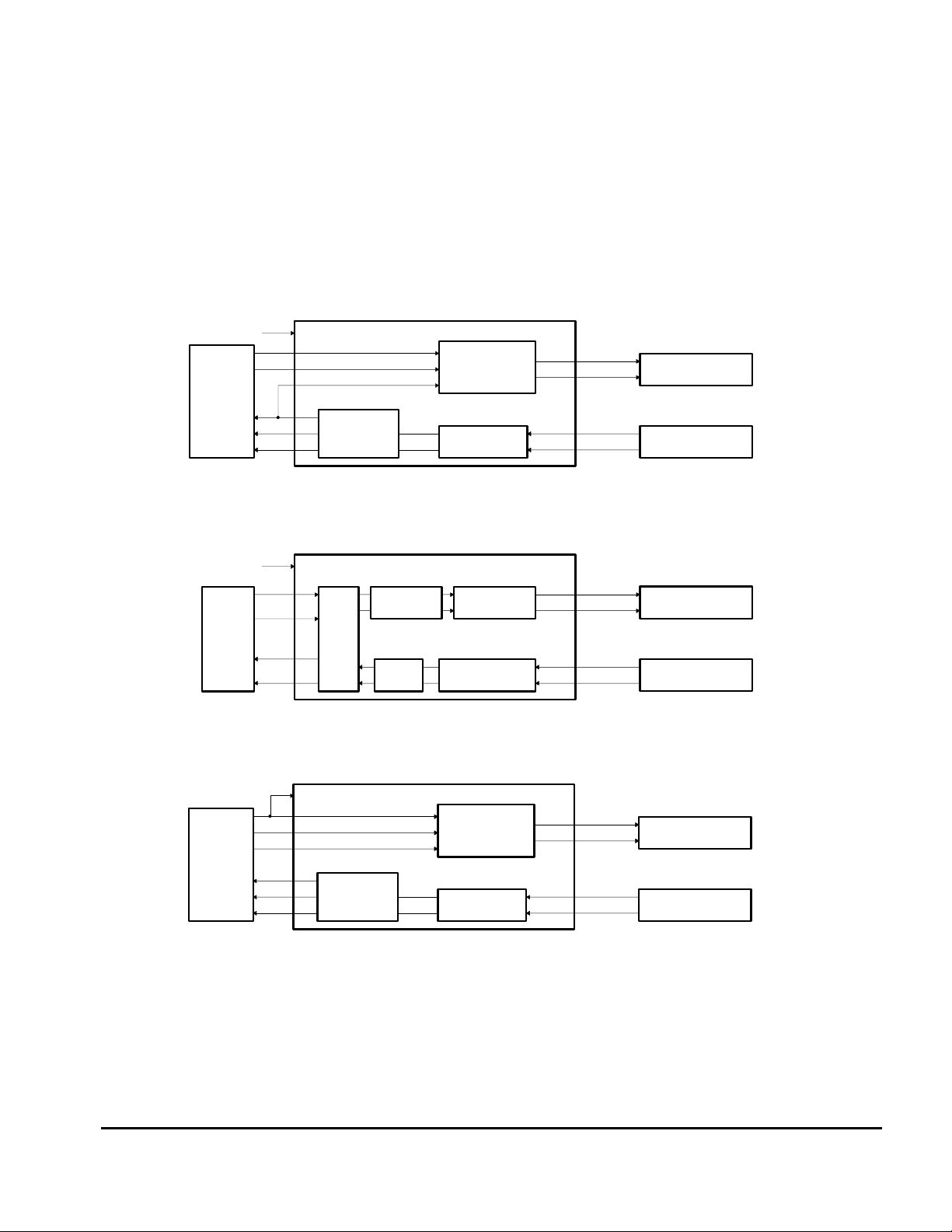
OVERVIEW OF APPLICATIONS
This section summarizes a typical application of the
AK61584 in various environments, and discusses
what AK61584 options would normally be selected
in that application. See Figure 8.
AT&T 62411 APPLICATION
(Systems with a single T1 line)
12.352MHz ±32ppm
TPOS
TNEG
CS2180B
FRAMER
CIRCUIT
TCLK
RCLK
RPOS
RNEG
REFCLK
JITTER
ATTENUATOR
AK61584
AT&T 62411 Customer Premises Application
AT&T 62411 applies at the T1 interface between
the customer premises and the carrier, and must be
implemented by the customer premises equipment.
LINE DRIVER
LINE RECEIVER
TTIP
TRING
RTIP
RRING
[AK61584]
TRANSMIT
TRANSFORMER
RECEIVE
TRANSFORMER
12.352MHz ±100ppm
TDATA
TCLK
(gapped)
MUX
RCLK
RDATA
CS2180B
FRAMER
CIRCUIT
Figure 8. Configuration Examples for Various Applicatons
ASYNCHRONOUS MUX APPLICATION
(for example, VT 1.5 card for SONET or SDH mux)
REFCLK
AMI
B8ZS
HDB3
CODER
(including 62411 systems with multiple T1 lines)
REFCLK
JITTER
ATTENUATOR
AK61584
JITTER
ATTENUATOR
AIS
DETECT
SYNCHRONOUS APPLICATION
AK61584
LINE DRIVER
LINE RECEIVER
LINE DRIVER
LINE RECEIVER
TTIP
TRING
RTIP
RRING
TTIP
TRING
RTIP
RRING
TRANSMIT
TRANSFORMER
RECEIVE
TRANSFORMER
TRANSMIT
TRANSFORMER
RECEIVE
TRANSFORMER
0185-E-00
-12-
98/04
Page 13

ASAHI KASEI
In 62411 applications, an overriding design consideration is management of jitter. Typically, the AK61584
will use it's jitter attenuator on the receive side to reduce the jitter seen by the system synchronizer. The
transmit clock presented to the AK61584 by the system
will be Stratum 4 quality or better, and is input to both
the reference clock pin and
independent
jitter on the reference clock must be well below the
the
clock source is used for the reference clock,
jitter allowed by 62411.
Category I Asynchronous Multiplexer
Application
transmit clock pin. If an
[AK61584]
Category II Synchronous Application
A typical example of a category II application is a T1
card of a central office switch or a 0/1 digital
cross-connect system. These systems use receive side
jitter attenuation to reduce the jitter presented to the
system, and will use a Stratum 3 or better system clock
to feed the AK61584 transmit and reference clocks. In
these systems, a single hardware design can support T1
and/or E1 under software control since the rate of the
transmit/reference clock rate will be varied by the system to match the line rate(T1 or E1).
Asynchronous multiplexers take multiple T1/E1 lines
(which are asynchronous to each other), and combine
them into a higher speed
transmission rate. Examples
are M13 muxes, and SONET muxes. In these systems,
the jitter attenuator is used on the transmit side of the
AK61584 to remove the waiting time jitter caused by
the multiplexer. Because the transmit clock is jittered,
the reference clock to the AK61584 will be provided by
an external quartz crystal, which operates at the 1-X or
8-X data rate. T1/E1 framers are typically not required
in asynchronous multiplexers, so the B8ZS/
AMI/HDB3 coders in the AK61584 are activated.
C C C
O
O O
N
N N
2 1 0
0 0 0
0 0 1
0 1 0
0 1 1
1 0 0
1 0 1
1 1 0
TRANSMITTER
Pulse Width at Pulse Shape
50% amplitude
244 ns(50%) E1:square, 2.37 Volts into 75ohm
244 ns(50%) E1:square, 3.00 Volts into 120ohm
350 ns(54%) DSX-1:0-133ft
350 ns(54%) DSX-1:133-266ft
350 ns(54%) DSX-1:266-399ft
350 ns(54%) DSX-1:399-533ft
350 ns(54%) DSX-1:533-655ft
TRANSMITTER
The transmitter takes data from a T1 or E1 terminal,
and produces pulses of appropriate shape. The transmit
clock (TCLK) and transmit data (TPOS & TNEG, or
TDATA) are supplied synchronously. Data is sampled
on the falling edge of the input clock.
Pulse shaping and signal level are determined by configuration inputs as shown in Table 1. Typical output
pulses are shown in Figures 9 and 10.
RECEIVER
Slicing
Level
50%
50%
65%
65%
65%
65%
65%
Coder
AMI/HDB3
AMI/HDB3
AMI/B8ZS
AMI/B8ZS
AMI/B8ZS
AMI/B8ZS
AMI/B8ZS
CON3 must be set to 0.
Table 1. Configuration Selection
0185-E-00 98/04
-13-
Page 14

ASAHI KASEI
269 ns
(244 + 25)
20%
V = 100%
Figure 9. Typical Pulse Shape at DSX-1 Cross Connect Figure 10. Mask of the Pulse at 2048kbps Interface
50%
0%
10% 10%
20%
10% 10%
Note – V corresponds to the nominal peak value.
194 ns
(244 – 50)
244 ns
219 ns
(244 – 25)
20%
488 ns
(244 + 24 4)
[AK61584]
Nominal pulse
10% 10%
14
The line driver internally matches the impedance of the
line load, providing 14 dB of return loss during the
transmission of both marks and spaces. This improves
signal quality by minimizing reflections off the transmitter. Internal impedance matching reduces current
consumption by factor of nearly two compared to return
loss achieved by external resistors.
The transmitter provides for all ones insertion at the
frequency of REFCLK. Transmit all ones is selected
when TAOS goes high, and causes continuous ones to
be transmitted on the line (TTIP and TRING). In this
mode, the TPOS and TNEG, or TDATA, inputs are ignored.
When any transmit control pin (TAOS, LLOOP, or
CON<0-2>) is toggled, the transmitter stabilizes within
22 bit periods. The transmitter will take longer to stabilize when RLOOP is selected because the timing circuitry must adjust to the new frequency.
Recommended transmitter transformer specifications
are shown below:
When the transmitter transformer secondaries are
shorted via a 0.5ohm resistor, the transmitter will out-
put a maximum of 50 mA-rms, as required by the British OFTEL OTR-0001 specification.
Turns ratio 1:2 step-up for TX(T1)
1:2 step-down for RX(T1)
1:1.32 step-up for TX(E1)
1:1.32 step-down for RX(E1)
Primary inductance 1.5 mH min measured at
772 kHz
Primary leakage
Inductance
Secondary leakage
0.3 uH max at 772 kHz
with secondary shorted
0.4 uH max at 772 kHz
Inductance
Interwinding
Capacitance
18 pF max, primary to
secondary
ET-constant 16 V-us min
Table 2(a). Transformer Requirements
Turns Ratio Part# Manufacturer
1:2(T1) PE-65351
4023
1:1.32(E1) 67148170
4022
Pulse Engineering
JPC Corporation
Schott Corporation
JPC Corporation
Table 2(b) Recommended Transformer
0185-E-00 98/04
-14-
Page 15

ASAHI KASEI
[AK61584]
RECEIVER
The receiver extracts data and clock from the T1/E1
signal and outputs clock and synchronized data. The
receiver can receive signals over the entire range of
short haul cable lengths.
The clock recovery circuit is a second-order phase
lock loop, and can tolerate as much as 0.4U1 of jitter
from 10 kHz to 100kHz, without error (Figure 11). The
clock and data recovery circuit is tolerant of long strings
of consecutive zeros, and will successfully receive a
1-in-175, jitter- free input signal.
300
100
10
PEAK-TO-PEAK
JITTER
(unit intervals)
0.1
1
AT&T62411
(1990 Version)
1 10 100 300 700 1k 10k 100k
JITTER FREQUENCY(Hz)
Figure 11. Minimum Input Jitter Tolerance of Receiver
(Clock Recovery Circuit and Jitter Attenuator)
AK61584
Performance
Data at RPOS and RNEG, is stable and may be
sampled using the recovered clock. CLKE determines
the clock polarity for which output data is stable and valid
as shown in Table 3. When CLKE is high, RPOS and
RNEG are valid on the falling edge of RCLK. When
CLKE is low, RPOS and RNEG are valid on the rising
edge of RCLK. In Hardware mode, the CLKE selection is made via pin 27. In host mode, the CLKE selection
is mode via control register (Channel 1 Control A, bit 7).
CLKE DATA CLOCK Clock edge for
valid data
LOW RPOS
RNEG
HIGH RPOS
RNEG
RCLK
RCLK
RCLK
RCLK
Rising
Rising
Falling
Falling
Table 3. Data Output/Data relationship
The signal is detected differentially across the receive
transformer. Recommended receiver transformer
specifications are identical to the transmit transformer
specifications.
Receiver Loss of Signal
The receiver will indicate loss of signal upon receiving 175+/-15 consecutive zeros. A digital counter
counts received zeros, based on recovered clock cycles. The receiver reports loss
appropriate
Loss of Signal pin, LOS high. The LOS
of signal by setting the
condition is exited using the ANSI T1.231- 1993 criteria,
namely 12.5% ones density for175+/-75 bit periods with
no more than 100
zeros in a row.
If a loss of signal condition occurs when the host mode is
being used, the LOS and LOS-latched bits will be set
and an interrupt will be issued. LOS will go low (and flag
the interrupt pin again, if the serial I/O is used) when a
valid signal is detected. The LOS-latched bit will stay high
until read, and then will remain low until the next loss
of signal event occurs. See Figure 12. Note that in the
hosts mode serial port operation, LOS is simultaneously available from both the register and pin LOSx.
LOS Currently Active
(LOS bit & LOS pin)
Latched LOS
(Latch LOS bit)
Interrupt
(INT)
Read LOS bits
"Short" LOS event
Set by start of LOS
Set by Change of LOS
Cleared by Read
Cleared by Read
"Long" LOS event
Figure 12 Loss of Signal Event Relationship
0185-E-00 98/04
-15-
Page 16

ASAHI KASEI
When the jitter attenuator is in the receive path, upon loss
of signal, the frequency of last recovered signal is
held over. When the jitter attenuator is not in the receive path, the last recovered frequency is not held over,
Rather, the output frequency will become the frequency of the reference clock.
Any time a channel is reset or powered down, (for
example by RESET, PD1, PD2, or power-on reset),
the loss of signal indicator on that channel is set high.
The loss of signal indicator remains high until data is
recovered by the receiver.
[AK61584]
Receiver AIS Detection
The receiver detects AIS upon observation of
99.9% ones density for 5.3 ms. More specifically, the AIS
detection criteria is less than 9 zeros out of 8192 bits.
When AIS is detected, the AK61584 sets the control
register bits AIS and Latched-AIS, high. In the coder
mode, the receiver also sets output pin AIS high. The
end of the AIS condition occurs when
> 9 zeros are
detected out of 8192 bits. The AIS bits in the status
register operate the same as the LOS bits (see Table5) upon detecting AIS. When a channel is powered
down, all indications are forced low.
JITTER ATTENUATOR
The jitter attenuator can be switched into either the receive
or transmit paths. Alternatively it can be removed from
both paths (thereby decreasing propagation delay).
Atten0x Atten1x Location of
Jitter Attenuator
0 0 Receiver
0 1 Transmitter
1 0 Neither
1 1 Reserved
Table 4. Jitter Attenuation Control
In hardware mode, the location of the attenuators is the
same for channel 1 and 2, and is controlled by pins
ATTEN0 and ATTEN1. See Table4. In host modes,
Figure 13. Typical Jitter Transfer Function
the location of the attenuators is programmable on a
per-channel basis, using bits ATTEN01 and
ATTEN11 for channel 1, and bits ATTEN02 and
ATTEN12 for channel 2. The control bits also conform
to Table 4.
A typical jitter attenuation curve is shown in Figure 13.
The attenuator consists of a 64-bit FIFO, a narrow-band monolithic PLL, and control logic. Signal
jitter is absorbed in the FIFO. The FIFO is designed to
neither overflow nor underflow. If overflow or underflow is imminent, the jitter transfer function is altered to
insure that no bit errors occur. Under this circumstance, jitter gain may occur, and jitter should be attenuated externally in a frame buffer. The jitter attenuator will typically tolerate 43 UIs before the overflow/underflow
mechanism takes effect. Before the jitter attenuator has
had time to “lock” to the average incoming frequency,
for example, after a chip reset, the attenuator will tolerate
a minimum of 22 UIs before the overflow/underflow
mechanism takes effect.
For T1/E1 line cards employed in high-speed multiplexers (e.g.,SONET and SDH), the jitter attenuator is typically used in the transmit path. The attenuator
can be fed a gapped transmit clock, with gaps 22 UIs,
and transmit clock burst rate <8 MHz.
0185-E-00 98/04
-16-
Page 17

ASAHI KASEI
CODER MODE
In the coder Mode, three line codes are available: AMI,
B8ZS and HDB3. The input to the encoder is T DATA.
The outputs from the decoder are RDATA and BPV
(Bipolar Violation Strobe). In host modes, the encoder
and decoder are selected using control register bits
CODER (1 =coder active, 0 = transparent mode, coder
disabled) and AMI-T/AMI-R (1 =AMI, 0 =B8ZS or
HDB3) where the transmitter and receiver can be ind ependently controlled. The selection of B8ZS versus
HDB3 is made by the control bits: CON<0:3>. In
hardware mode, the encoder and decoder are controlled
simultaneously by pins CODER1 and CODER2 (1
=coder active, 0 =transparent mode, coder disable). The
line code is B8ZS or HDB3. The selection of B8ZS
versus HDB3 is made by the pins: CON<0:2>.
In the coder mode, the receiver sets output pins AIS1
and AIS2 high, when AIS is detected, respectively on
channels 1 and 2.
[AK61584]
LOOPBACKS
Local Loopbacks
The two local loopbacks take clock and data presented
on TCLK, TPOS, and TNEG, or TDATA and outputs it at RCLK, RPOS and RNEG, or RDATA. As
shown in the block diagram on the first page of the data
sheet, loopback 1 includes the jitter attenuator. Loopback 2 includes the line driver and the receiver.
For both local loopbacks, inputs to the transmitter are
still transmitted on the line, unless TAOS has been selected in which case, AMI-coded continuous ones are
transmitted to the line at the rate determined by TCLK.
Receiver inputs are ignored when local loopback is in
effect. Local loopback 1 is selected by a control pin,
or a control bit. Loopback 2 is selected only via a control bit.
Remote Loopback
In the coder mode, pin BPV goes to a logic 1 for one bit
period when a bipolar violation is detected i n the received
signal. B8ZS (or HDB3) zero substitutions are not
flagged as bipolar violations if the B8ZS (or HDB3)
decoder has been enabled. A latched-BPV indication is also available in the status register.
REFERENCE CLOCK
The AK61584 requires a T1 or E1 reference clock.
This clock is input on pin REFCLK, and can be either
a 1-X clock (i.e.,1.544 MHz or 2.048 MHz), or a 8-X
clock (i.e.,12.352 MHz or 16.384 MHz). pin 1XCLK
determines which option is used (active high for 1-X, and
low for 8-X).
Any jitter present on the reference clock will not be filtered
by the jitter attenuator, and will be present on the output
of the jitter attenuator. The reference clock should have a
minimum accuracy of 100 ppm.
In remote loopback, the recovered clock and data input
on RTIP and RRING are sent back out on the line via
TTIP and TRING as shown in the block diagram on
the front page of this data sheet. The recovered incoming signals are also sent to RCLK, RPOS and
RNEG, or RDATA. A remote loopback may be selected
in both the hardware and host modes. Simultaneous selection of local and remote loopback modes is not valid.
POWER DOWN
The PD1 and PD2 pins reset, respectively, the transmitter, receiver and jitter attenuator of channels 1 and 2.
Whenever PD1 or PD2 is selected, the selected channel
remains powered down, and the outputs (pins RCLK,
RPOS, RNEG, RDATA, BPV, AIS, TTIP, and TRING)
associated with that channel are put into a
high-impedance state, and pin LOS is set high. Additionally, the status register bits are reset. The control,
mask, and arbitrary waveform registers are unchanged.
0185-E-00 98/04
-17-
Page 18

ASAHI KASEI
[AK61584]
The non-selected channel operates normally. Selecting
PD1 or PD2 does not reset the AK61584 control registers, or serial control ports. Simultaneously selecting
PD1 and PD2 will power down some additional
analog circuitry that is shared by both channels. After
exiting the power down state, the channel will be fully
operational in less than 20 ms.
RESET
In operation, the AK61584 is continuously calibrated,
making the performance of the device independent
of power supply or temperature variations. The
continuous calibration function forgoes any requirement
to reset the line interface when in operation.
The RESET pin resets the entire device, including the
control logic, and clears all control and mask registers.
A reset event results in the Latched-reset bit being set in
the Status register. A reset request can be made by
setting RESET high for at least 200 ns. Reset will initiate on the falling edge of RESET. The reset operation
takes less than 20 ms to complete. Upon exiting
RESET, both channels are powered up.
POWER ON RESET
CONTROL
Control of the AK61584 is via either host mode (register read/write via serial control port), or hardware mode
(individual control pin). Hardware mode offers significantly
fewer programmability options than the host mode.
The following pins are used to select the mode. The
MODE pin active low selects Hardware mode. The
MODE pin active high enables host mode. Once host
mode is invoked, the pin 16 must be set to logic low. The
definition of the pins in each mode is shown in the
block diagram of the first page of the data sheet.
Hardware Mode
The following control options are available in Hardware mode on a per channel basis: power down, remote
loopback, transmit all ones, coder mode, line length
selection and location of jitter attenuator.
Host Modes
Host mode allows a microcontroller to read/write ten
AK61584 control and status registers. The registers
are defined in Table 5, and discussed in a later section.
Host mode interface ports are available for serial.
Upon power-up, the IC is held in a static state until the
supply crosses a threshold of approximately 60% of the
power supply voltage. When this threshold is crossed, the
device will delay for about 10 ms to allow the power
supply to reach operating voltage. After this delay, calibration of the transmit and receive sections commences.
The calibration can take place only if REFCLK and
TCLK are present. The initial calibration takes less
than 20 ms. The power-on reset has the same effect as the
RESET. A power-on reset event results in the Latched-reset
bit being set in the Status register.
0185-E-00 98/04
In host mode, the AK61584 registers occupies a
six-bit address space, where those six bits select a
register in the range h10 to h19.
The AK61584 generates an interrupt on pin INT
whenever a status register changes. The polarity of the
INT pin is programmable. When the IPOL pin is high,
INT goes high to generate a processor interrupt.
When the IPOL pin is low, INT goes low to generate
a processor interrupt.
-18-
Page 19

ASAHI KASEI
[AK61584]
REGISTERS
The control and status registers are defined in Table 5,
and are accessible in host mode. Each channel has its
own set of Status, Mask and Control. The status register
is read-only. Writing to the status register has no impact on
its contents. Interrupts are generated on the INT pin every
time a status register changes. Reading a status register
resets all bits i n that status register to 0. The mask register allows the user to mask interrupts on a status
register on a per-bit basis. The control registers select features /functionality.
Status Registers Description
Each bit in the status register is defined below.
AIS and Latched-AIS: Indicates an all-ones condition.
AIS is set high while AIS condition is currently detected. Latched-AIS indicates that a AIS condition has
occurred since the last read of the status register.
Interrupt: Indicates that the status register has changed
sometime since the last read of the status register.
Latched-BPV: indicates a bipolar violation event has
been detected in the receiver sometime since the last
read of the status register. This bit is set only when the
line-code decoder is enabled.
Latched-Overflow: Indicates that a waveform generated
using the Arbitrary Waveforms has exceeded full scale
sometime since the last read of the status register.
(Optional information, refer to the Application Note.)
LOS and Latched-LOS : Indicates loss of signal
condition. LOS is set high while LOS condition is
currently detected. Latched-LOS indicates that a
LOS condition has occurred since the last read of
the status register.
Latched-reset: Indicates that a reset event
(power-up or manual) has occurred since the last read
of the status register. This status bit is not maskable.
Address
h10
b0000
h11
b0001
Bit Name
Channel 1 Status
7
LOS1
6
Latched-LOS1
5
AIS1
4
Latched-AIS1
3
Latched-BPV1
2
Latched
-Overflow1
1
Latched-reset
0
Interrupt1
Channel 2 Status
7
LOS2
6
Latched-LOS2
5
AIS2
4
Latched-AIS2
3
Latched-BPV2
2
Latched
-Overflow2
1
reserved
0
Interrupt2
Definition ResetRegister
1 0 Value
LOS currently detected
LOS event since last read
AIS currently detected
AIS event since last read
BPV event since last read
Pulse overflow since last
Read
Reset event since last read
Interrupt event since last
Read
LOS currently detected
LOS event since last read
AIS currently detected
AIS event since last read
BPV event since last read
Pulse overflow since last
Read
Interrupt event since last
Read
Table 5(a). Status Registers
no LOS
no LOS
no AIS
no AIS
no BPV
no overflow
no reset
no interrupt
no LOS
no LOS
no AIS
no AIS
no BPV
no overflow
no interrupt
1
1
0
0
0
0
1
0
1
1
0
0
0
0
0
0
0185-E-00 98/04
-19-
Page 20

ASAHI KASEI
[AK61584]
Address
h10
b0010
h11
b0011
Bit Name
Channel 1 Mask
7
Mask LOS1
6
Mask LatchedLOS1
5
Mask AIS1
4
Mask LatchedAIS1
3
Mask LatchedBPV1
2
Mask Latched
-Overflow1
1
reserved
0
Mask
Interrupt1
Channel 2 Mask
7
Mask LOS2
6
Mask LatchedLOS2
5
Mask AIS2
4
Mask LatchedAIS2
3
Mask LatchedBPV2
2
Mask Latched
-Overflow2
1
reserved
0
Mask
Interrupt2
1 0 Value
Mask status bit 7
Mask status bit 6
Mask status bit 5
Mask status bit 4
Mask status bit 3
Mask status bit 2
Mask status bit 0 &
Interrupt pin
Mask status bit 7
Mask status bit 6
Mask status bit 5
Mask status bit 4
Mask status bit 3
Mask status bit 2
Mask status bit 0 &
Interrupt pin
Definition ResetRegister
Enable status bit 7
Enable status bit 6
Enable status bit 5
Enable status bit 4
Enable status bit 3
Enable status bit 2
Enable status bit 0 &
Interrupt pin
Enable status bit 7
Enable status bit 6
Enable status bit 5
Enable status bit 4
Enable status bit 3
Enable status bit 2
Enable status bit 0 &
Interrupt pin
0
0
0
0
0
0
0
0
0
0
0
0
0
0
0
0
Note)Mask LOS and Mask Latched-LOS need to controlled simultaneously, and Mask AIS and Mask
Latched-AIS also.
Table 5(b). Mask Registers
Mask Registers Description
AMI-T: Writing a “0” enables the B8ZS or HDB3
encoder in the transmit path. B8ZS vs. HDB3 seWriting a “1” to a bit of the mask register forces the corresponding bit of the status register to stay fixed at “0”.
Control A Registers Description
lection is determined by the CON<0:2> bits. Writing
a “1” enables the AMI encoder.
CLKE: When CLKE is set to “1”. RPOS and
RNEG are valid on the falling edge of RCLK.
Each bit in the control register is defined below.
When CLKE is set to “0”, RPOS and RNEG are
valid on the rising edge of RCLK. This bit conAMI-R: Writing a “0”enables the B8ZS or HDB3
decoder in the receiver path. B8ZS vs. HDB3 selection is determined by the CON<0:2> bits. Writing
trols the RPOS/RNEG polarity for both host
modes. The CLKE pin provides the same function-
ality for the hardware mode.
a “1” enables the AMI decoder.
0185-E-00 98/04
-20-
Page 21

ASAHI KASEI
[AK61584]
Address
h14
b0100
h15
b0101
bit Name
Channel 1 Control A
76CLKE
PD1
5 ATTEN01 ATTEN01 ATTENN11 0
4 ATTEN11 0
3
CODER1
2
AMI-T1
1
AMI-R1
0
Factory Test 1
Channel 2 Control A
76Reserved
PD2
5 ATTEN02 ATTEN02 ATTEN12 0
4 ATTEN12 0
3
CODER2
2
AMI-T2
1
AMI-R2
0
Factory Test
Definition ResetRegister
1 0 Value
RPOS/RNEG valid on
Falling RCLK
Power Down Channel 1
0
0
1
Coder/Mode enabled
AMI encoder enabled
AMI decoder enabled
Test
Must be set to 0
Power Down Channel 2 Power Up Channel 2
0
1
Coder/Mode enabled
AMI encoder enabled
AMI decoder enabled
Test
1
0
0
1
0
RPOS/RNEG valid on rising
RCLK
Power Up Channel 1
Attenuator 1 in receiver path
Attenuator 1 in transmit path
Attenuator 1 inactive
Transparent mode enabled
B8ZS/HDB3 encoder enabled
B8ZS/HDB3 decoder enabled
Normal Operation
Attenuator 2 in receiver path
Attenuator 2 in transmit path
Attenuator 2 inactive
Transparent mode enabled
B8ZS/HDB3 encoder enabled
B8ZS/HDB3 decoder enabled
Normal Operation
0
0
0
0
0
0
0
0
0
0
0
0
0
0
Table 5(c). Control A Registers
CODER: Writing a “1” enables a coder (AMI,
B8ZS or HDB3), and enables pins TDATA, RDATA,
AIS and BPV. Writing a “0” disables the coder, placing the channel in transparent mode, and enables pins TPOS,
TNEG, RPOS and RNEG.
Factory Test: Must be set to “0” for normal operation.
PD: Writing a “1” powers down the channel.
Control B Registers Description
Each bit in the control register is defined below.
CON<0:2>: controls the configuration of the transmitter, receiver and coder as shown in Table 1. Both
channels must operate at the same rate (both T1 or
both E1). Specifications are not guaranteed with the
channels operating at different rates. After a manual or
power-on reset, the CON bits are reset to the E1 rate.
If a single channel T1 mode is desired (i.e., second
channel is not used), it is recommended that both channels be set to the T1 rate.
LLOOP1: Writing a “1” enables local loopback #1,
as shown in the block diagram on the front page of the
data sheet.
LLOOP2: Writing a “1” enables local loopback #2,
as shown in the block diagram on the front page of the
data sheet.
RLOOP: Writing a “1” enables remote loopback
for this channel.
TAOS: Writing a “1” enables transmit all ones.
0185-E-00 98/04
-21-
Page 22

ASAHI KASEI
[AK61584]
Definition ResetRegister
disable transmit all ones
disable remote loopback
disable loopback #1
disable loopback #2
disable transmit all ones
disable remote loopback
disable loopback #1
disable loopback #2
Address
h16
b0110
h17
b0111
Bit Name
Channel 1 Control B
7
TAOS1
6
RLOOP1
5
LLOOP11
4
LLOOP21
3
CON31
2
CON21
1
CON11
0
CON01
Channel 2 Control B
7
TAOS2
6
RLOOP2
5
LLOOP12
4
LLOOP22
3
CON32
2
CON22
1
CON12
0
CON02
1 0 Value
Enable transmit all ones
Enable remote loopback
Enable local loopback #1
Enable local loopback #2
Must be set to 0
See Table 1
See Table 1
See Table 1
Enable transmit all ones
Enable remote loopback
Enable local loopback #1
Enable local loopback #2
Must be set to 0
See Table 1
See Table 1
See Table 1
Table 5(d). Control B Registers
Note) CON3 is used for Arbitrary Waveform Generation. Please connect to 0 for the normal operation.
0
0
0
0
0
0
0
0
0
0
0
0
0
0
0
0
Register
Address
h18
b1000
h19
b1001
Bit Name
Channel 1 Arbitrary Pulse Shape
7
MSB
6
5
4
3
2
1
0
LSB
Channel 2 Arbitrary Pulse Shape
7
MSB
6
5
4
3
2
1
0
LSB
Table 5(e). Arbitrary Waveform Registers
Definition Reset Value
Undefined
Undefined
Undefined
Undefined
Undefined
Undefined
Undefined
Undefined
Undefined
Undefined
Undefined
Undefined
Undefined
Undefined
Undefined
Undefined
0185-E-00 98/04
-22-
Page 23

ASAHI KASEI
[AK61584]
7
(MSB)
BM
0
individual
Burst
1
6
ADD5 ADD3ADD4
(MSB)
5
Don't care
Figure 14. Address Command Byte (AC B)
43
ADD2
Register Address Field
HOST MODE REGISTER ACCESS
This mode is selected by setting pin MODE to
logic high, and pin 16 must be set to logic low. In the host
mode, the on-board registers can be written to via
the SDI pin or read from via the SDO pin at the clock
rate determined by SCLK. Through these registers, a
host controller can be used to control operational char acteristics and monitor device status. The serial port
read/write timing is independent of the system transmit
and receive timing.
Any read or write to the serial port is initiated by setting
Chip Select (CS) low and writing an 8-bit address/command byte (ACB). The ACB consists
of the three separate fields including a 6 -bit register
address (see Figure 14). The ACB is followed by a
data word.
In the ACB, D0(LSB) is the R/W field, and
specifies whether the current operation is to be a read or
a write: 1 = read, 0= write. The next 4 bits (D1-D4)
contain the address field. They specify which of the
registers to access. D5 and D6 are “don’t care bits”.
Setting bit D7 to 1 selects burst mode (described
below).
Registers h10 to h17 are read and written as described
above. Registers h18 and h19 are used to access multiple bytes for the arbitrary waveform generation, refer
to the AK61584 Application Note.
0
21
ADD1 ADD0 R/W
(LSB)
(LSB)
Write
0
Read
1
Another communication option, burst mode, is
available. Burst mode is specified by setting bit
D7(MSB) of the ACB to 1. Burst mode allows
multiple registers to be consecutively read or written.
Writing all registers allows fast initialization at
power-up or system reset. When using burst mode, the
address field of the ACB command word must be h00.
The registers are read or written in address order h10 to
h11, followed by 42 byte reads or writes to register
h18, followed by 42 bytes read or writes to register
h19. Burst mode ends on the first rising edge of CS,
and may be ended at any time. If a burst write ends
before writing 92 bytes, the remaining, unwritten
bytes are unchanged.
Figure 15 shows the timing relationships for data
transfers. When the SPOL pin is high, data on SDO is
valid on the falling edge of SCLK. When the SPOL
pin is low, data on SDO is valid on the rising edge
of SCLK.
All data is written to and read from the port LSB
first. When writing to the port, SDI input data is sampled on the rising edge of SCLK.
SDO goes to high impedance state when not in use.
SDO and SDI may be tied together in applications
where the host processor has a bi-directional I/O
port.
CS
SCLK
SDI
SDO
R/W 0
0185-E-00 98/04
0
00
Address/Command Byte
Figure 15. Serial Read/W rite Timing
1
00
-23-
D0
D1
D2 D3
Data Input/Output
D0
D1 D2 D3 D4 D5 D6
D4 D5
D7
D6
D7
Page 24

ASAHI KASEI
y
)
g
[AK61584]
Arbitrary Waveform Registers
These registers are written multiple times to enter an
arbitrary waveform.
ARBITRARY WAVEFORM GENERATION
In additon to the predefined pulse shapes, the user can
create arbitrary pulse shapes using the host mode for
evaluation. Refer to the AK61584 Application Note.
POWER SUPPLY
The device operates from a single 3.3 Volt supply.
Separate pins for the various supplies provide internal
isolation. However, these pins should be connected externally with the power supply pins de-coupled to their
respective grounds. The various ground pins must not be
more negative than AGND.
De-coupling and filtering of the power supplies is crucial for the proper operation of the analog circuits. The
best way to configure the power supplies is to tie all
of the supply pins together at the chip. As shown in
Figure 1, a capacitor should be connected between
each supply and its respective ground. For the 1uF and
smaller capacitors, use mylar or ceramic capacitors and
place them as closely as possible to their respective
power supply pins. Wire-wrap bread boarding of
the line interface is not recommended because lead
resistance and inductance serve to defeat the func-
tion of the de-coupling capacitors. A 5kohm, 1%,
resistor should connect BGREF to ground.
JTAG BOUNDARY SCAN
JTAG boundary scan supports board testing. Using
boundary scan, the integrity of the digital paths between
ICs on a board can be verified. This verification
is supported by the ability to externally set the
signals on the AK61584's digital output pins, and to
externally read the signals present on the AK61584's
input pins.
As shown in Figure 16, the JTAG hardware consists o f
data and instruction registers plus a Test Access
Port (TAP) controller. Control of the TAP is achieved
through signals applied to the Test Mode Select
(J_TMS) and Test Clock (J_TCK) input pins. Data is
shifted into the registers via the Test Data Input
(J_TDI) pin, and shifted out of the registers via the Test
Data Output (J_TDO) pin, again using J_TCK. The
Instruction register defines which data register is
included in the shift operation. Note that if J_TDI
is left floating, an internal pull-up resistor forces
the pin high.
JTAG Data Registers (DR)
The test data registers are: the Boundary-Scan
Regiser (BSR), and the Bypass Register (BR).
J-TDI
J-TCK
J-TMS
Digital output pins
Parallel latched
Parallel latched
output
output
Boundary Scan Data Register
32bit Data Register(Factory use onl
Bypass Data Register
Instruction(shift) Register
Parallel latched
output
TAP Controller
ital input pins
Di
JTAG Block
MUX
J-TDO
Figure 16. JTAG Circuitry Block Diagram
0185-E-00 98/04
-24-
Page 25

ASAHI KASEI
[AK61584]
Boundary Scan Register: The BSR can be connected i n
parallel to all the digital I-O pins, and provides the
mechanism for applying/reading test patterns to/from
the board traces. The BSR is initialized and read
using the instruction SAMPLE/PRELOAD. The bit
ordering for the BSR is the same as the top-view packaged
pin out, counter-clockwise beginning with PD1 (pin 15)
and ending with LOS1 (pin 7), as shown in Table 6. The
analog, oscillator, power, ground, ATTEN0, CLKE
and MODE pins are not included as part of the
boundary-scan register. ATTEN0, CLKE and MODE are
not included because they are typically hard-wired to
power or ground on a board.
All output pins are 3-state pins (logic high, logic low or high
impedance); their value can be set via the
PRELOAD/EXTEST instructions. Since outputs
are all 3-state, 2 bits are required to specify the states of
each output pin in the BSR.The first bit (which is shifted
in first) contains the testing data which may be output on
the pin. The second bit, which is shifted in following the
first bit, selects between an output-enabled state (bit set to
1) or high-impedance state (bit set to 0). Thus, two
J_TCK cycles are required to load testing data for
each output pin.
Each input pin requires only 1 bit in the BSR.
The bi-directional pins, TNEG1/AIS1, TNEG2/AIS2,
INT/RLOOP1, LOS1, LOS2, LLOOP1/SCLK,
LLOOP2/SDO, TAOS1/SDI, TAOS2/SPOL, and the
CON<0:2> pins have three bits in the BSR. The first
bit shifted into the BSR captures the value of the pin.
This pin may have its value set externally (if the third bit
is 0) or set internally (if the third bit is 1). The second bit
shifted into the BSR sets the output value. This value is
output on the pin when the third bit is 1. The third bit configures the output driver as high-impedance (bit set to
0) or active (bit set to 1).
Note that the interrupt pin on the AK61584 has the
ability of being a active high or active low signal. In
host mode, the IPOL pin controls this functionality.
During JTAG testing in host mode, the polarity of the
INT pin will be determined by the state of the IPOL pin.
The INT pin on the AK61584 should not be configured
as an output by the JTAG BSR if the device is in hardware mode. Likewise, the INT pin should not be config-
0185-E-00 98/04
ured as an input by the JTAG BSR if the device is in
host mode.
Thus, the entire BSR is 62 bits long.
BSR
bits
1 PD1 15 input
2 IPOL,RLOOP2 33 input
3 PD2 34 input
4 CODER2 41 input
5-7 LOS2 42 bi-directional
8-10 TNEG2,AIS2 43 bi-directional
11 TPOS2,TDATA2 44 input
12 TCLK2 45 input
13-14 RNEG2,BPV2 46 output
15-16 RPOS2,RDATA2 47 output
17-18 RCLK2 48 output
19 CODER1 49 input
20 CON22 50 input
21-23 CON21 51 bi-directional
24-26 CON12 52 bi-directional
27-29 CON11 53 bi-directional
30-32 CON02 54 bi-directional
33-35 CON01 58 bi-directional
36-38 TAOS2 59 bi-directional
39-41 SDI,TAOS1 60 bi-directional
42-44 SDO,LLOOP1 61 bi-directional
45 SCLK,LLOOP2 62 input
46-48 INT,RLOOP1 63 bi-directional
49 CS,ATTEN1 64 input
50-51 RCLK1 1 output
52-53 RPOS1,RDATA1 2 output
54-55 RNEG1,BPV1 3 output
56 TCLK1 4 input
57 TPOS1,TDATA1 5 input
58-60 TNEG1,AIS1 6 bi-directional
61-63 LOS1 7 bi-directional
Table 6 Boundary Scan Register Contents
Bypass Register: The Bypass register consists of a single
bit, and provides a serial path between J_TDI and J_TDO,
bypassing the BSR. The provision of this register allows
the bypassing of those segments of the board-level serial
test register which are not required for a specific test. This
also reduces test access times, by reducing the total number of shifts required from J_TDI to J_TDO.
-25-
Pin
Name
PIN#Pad
Type
Page 26

ASAHI KASEI
[AK61584]
JTAG Instructions and Instruction Register
(IR)
The instruction register (2 bits) allows the instruction
to be shifted into the circuit. The instruction is
used to select the test to be performed or the data
register to be accessed or both. The valid instructions
are (LSB shifted in first):
IR CODE INSTRUCTION
00 EXTEST
01 SAMPLE/PRELOAD
11 BYPASS
EXTEST Instruction: The EXTEST instruction
allows testing of off-chip circuitry and board-level
interconnect. EXTEST connects the BSR to J_TDI
and J_TDO. The normal path between the
AK61584 logic and it's IO pins is broken; the signals on the output pins are loaded from the BSR; the
signals on the input pins are loaded into the BSR.
SAMPLE/PRELOAD Instruction: The
SAMPLE/PRE-LOAD instructions allows scanning of
the boundary-scan register without interfering with the
operation of the AK61584. This instruction connects
the BSR to J_TDI and J_TDO. The normal path between the AK61584 logic and its IO pins is maintained; the signals on those IO pins is maintained; the
signals on those 10 pins are loaded into the BSR. Additionally, this instruction can be used to latch values
into the digital output pins.
BYPASS Instruction: The BYPASS instruction
connects the minimum length, Bypass register
between J_TDI and J_TDO, and allows data to
be shifted in the shift-DR controller state.
Internal Testing Considerations
Note that the INTEST instruction is not supported because of the difficulty of performing significant internal
tests using JTAG. The most complete internal test
would involve inputting digital data on pins TCLK,
TPOS, TNEG, activating local loopback#2, and
reading that same data out on pins RCLK, RPOS
and RNEG. This test would include the full
transmit path, the full receive path, and optionally, the
jitter attenuator, and provides excellent test coverage of
the functional blocks. However, this test is difficult to implement for two reasons.
First, TCLK and REFCLK must be clocked at specific
frequencies, e.g., T1/E1+/-200 ppm for TCLK. If
these frequency requirements are not met, the performance of the transmitter, clock recovery circuit
and jitter attenuator is not guaranteed. If would be
difficult with JTAG to toggle the TCLK input at the
required rate.
Second, the loopback path includes two asynchronous
blocks, clock recovery and jitter attenuator. Therefore,
the exact time delay for a TPOS-input appearing on
RPOS-output is variable, making output signature
correlation difficult.
The one test that could be easily performed using an ar bitrary clock rate on TCLK and REFCLK is local
loopback#1, with jitter attenuator disabled. However,
that test provides such limited fault coverage, that is
only useful in determining if the device had been
catastrophically destroyed. Alternatively, catastrophic
destrucion of the IC and/or surrounding board traces
can be detected using EXTEST. Therefore, the INTEST instruction was viewed as providing little
significant incremental testing capability, while adding to product complexity, and was not included in
the AK61584.
JTAG TAP Controller
Figure 20 shows the state diagram for the TAP state
machine. A description of each state follows. Note
that the figure contains two main branches to access
either the data or instruction registers. The value
shown next to each state transition in this figure is
the value present at J_TMS at each rising edge of
J_TCK.
0185-E-00 98/04
-26-
Page 27

ASAHI KASEI
[AK61584]
Test-Logic-Reset State
In this state, the test logic is disabled so that normal operation of the device can continue unhindered. During
initialization, the AK61584 initializes the instruction
register.
No matter what the original state of the controller,
the controller enters Test-Logic-Reset state when the
J_TMS input is held high (logic 1) for at least five
rising edges of J_TCK. The controller remains in this
state while J_TMS is high. The AK61584 processor automatically enters this state at power-up.
Run-Test/Idle State
This is a controller state between scan operations. Once
in this state, the controller remains in this state as long as
J_TMS is held low. The instruction register and all test
data registers retain their previous state. When J_TMS is
high and a rising edge is applied to J_TCK, the
controller moves to the Select-DR state.
selected by the current instruction retains its previous state. If
J_TMS is held low and a rising edge is applied to
J_TCK when in this state, the controller moves into the
Capture-DR state, and a scan sequence for the selected
test data register is initiated. If J_TMS is held high
and a rising edge applied to J_TCK, the controller moves
to the Select-IR-Scan state.
The instruction does not change in this state.
Capture-DR State
In this state, the Boundary Scan Register captures input
pin data if the current instruction is EXTEST or
SAMPLE/PREROAD. The other test data registers,
which to not have parallel input, are not changed.
The instruction does not change in this state.
When the TAP controller is in this state and a rising
edge is applied to J_TCK, the controller enters the
Exit1-DR state if J_TMS is high or the Shift-DR state if
J_TMS is low.
Select-DR-Scan State
This is a temporary controller state. The test data register
1
0
Test-Logic-Reset
Run-Test/Idle
1
Select-DR-Scan
1
Capture-DR
0
0
Shift-DR
1
Exit1-DR
0
Pause-DR
0
1
Exit2-DR
1
Update-DR
1
1
0
1
0
Select-IR-Scan
1
Capture-IR
Exit1-IR
Pause-IR
0
Exit2-IR
0
0
Shift-IR
1
0
1
1
1
0
1
0
Update-IR
0
1
0
Figure 17. TAP controller State Diagram
0185-E-00 98/04
-27-
Page 28

ASAHI KASEI
Shift-DR State
In this controller state, the test data register connected
between J_TDI and J_TDO as a result of the current instruction shifts data on stage toward its serial output on
each rising edge of J_TCK.
The instruction does not change in this state.
When the TAP controller is in this state and a rising
edge is applied to J_TCK, the controller enters the
Exit1-DR state if J_TMS is high or remains in the
Shift-DR state if J_TMS is low.
[AK61584]
Exit2-DR State
This is a temporary state. While in this state, if
J_TMS is held high, a rising edge applied to J_TCK
causes the controller to enter the Update-DR state,
which terminates the scanning process. If J_TMS is
held low and a rising edge is applied t o J_TCK, the
controller enters the Shift-DR state.
The test data register selected by the current instruction retains its previous value during this state. The
instruction does not change in this state.
Exit1-DR State
This is a temporary state. while in this state, if J_TMS is
held high, a rising edge applied to J_TCK causes the
controller to enter the Update-DR state, which terminates the scanning process. If J_TMS is held low and a
rising edge is applied to J_TCK, the controller
enters the Pause-DR state.
The test data register selected by the current instruction retains its previous value during this state. This instruction
does not change in this state.
Pause-DR State
The pause state allows the test controller to temporarily
halt the shifting of data through the test data register in the
serial path between J_TDI and J_TDO. An example
use of this state could be to allow tester to reload its pin
memory from disk during application of a long test
sequence.
The test data register selected by the current instruction retains its previous value during this state. The
instruction does not change in this state.
The controller remains in this state as long as J_TMS
is low. When J_TMS goes high and a rising edge is
applied to J_TCK, the controller moves to the Exit2-DR
state.
Updata-DR State
The Boundary Scan Register is provided with a
latched parallel output to prevent changes at the parallel
output while data is shifted in response t o the EXTEST
and SAMPLE/PRELOAD instructions. When the
TAP controller is in this state and the Boundary Scan
Register is selected, data is latched onto the parallel
output of this register from the shift-register path on
the falling edge of J_TCK. The data held at the
latched parallel output does not change other than in
this state.
All shift-register stages in the test data register selected by
the current instruction retains their previous value during
this state. The instructions does not change in this state.
Select-IR-Scan State
This is a temporary controller state. The test data
register selected by the current instruction retains its
previous state. If J_TMS is held low and a rising edge
is applied to J_TCK when in this state, the controller
moves into the Capture-IR state, and a scan sequence
for the instruction register is initiated. If J_TMS is
held high and a rising edge is applied to J_TCK, the
controller moves to the Test-Logic-Reset state. The
instruction does not change in this state.
0185-E-00 98/04
-28-
Page 29

ASAHI KASEI
Capture-IR State
In this controller state, the shift register contained in the
instruction register loads a fixed value of “01” on the rising edge of J_TCK. this supports fault-isolation of the
board-level serial
test data path.
Data registers selected by the current instruction retain
their value during this state. The instruction does not
change in this state.
When the controller is in this state and a rising edge is applied to J_TCK, the controller enters the Exit1-IR state if
J_TMS is held high, or the Shift-IR state if J_TMS is
held low.
Shift-IR State
In this state the shift register contained in the instruction
register is connected between J_TDI and J_TDO and
shifts data one stage towards its serial output on each
rising edge of J_TCK.
The test data register selected by the current instruction retains its previous value during this state. The
instruction does not change in this state.
When the controller is in this state and a rising edge is applied to J_TCK, the controller enters the Exit1-IR state
if J_TMS is held high, or re-mains in the Shift-IR state if
J_TMS is held low.
Exit1-IR State
This is a temporary state. while in this state, if J_TMS
is held high, a rising edge applied to J_TCK causes the
controller to enter the Update-IR state, which terminates the scanning process. If J_TMS is held low and a
rising edge is applied to J_TCK, the controller enters the
Pause-IR state.
[AK61584]
Pause-IR State
The pause state allow the test controller to temporarily halt the shifting of data through the instruction
register.
The test data register selected by the current instruction retains its previous value during this state. The instruction does not change in this state.
The controller remains in this state as long as J_TMS is
low. When J_TMS goes high and a rising edge is applied to J_TCK, the controller moves to the Exit2-IR
state.
Exit2-IR State
This is a temporary state. While in this state, if J_TMS
is held high, a rising edge applied to J_TCK causes the
controller to enter the Update-IR state, which terminates the scanning process. If J_TMS is held low and a
rising edge is applied to J_TCK, the controller enters the
Shift-IR state.
The test data register selected by the current instruction retains its previous value during this state. The
instruction does not change in this state.
Updata-IR State
The instruction shifted into the instruction register
is latched onto the parallel output from the
shift-register path on the falling edge of J_TCK. Once
the new instruction has been latched, it becomes the current instruction.
Test data registers selected by the current instruction
retain their previous value.
JTAG Application Examples
The test data register selected by the current instruction retains its previous value during this state. The
instruction does not change in this state.
0185-E-00 98/04
Figures 18 and 19 show examples of updating the instruction register and data registers.
-29-
Page 30

ASAHI KASEI
[AK61584]
Figure 18.Test Logic Operation: Instruction Scan
0185-E-00 98/04
-30-
Page 31

ASAHI KASEI
[AK61584]
Figure 19. Test Logic Operation: Data Scan
0185-E-00 98/04
-31-
Page 32

ASAHI KASEI
PIN DESCRIPTION
[AK61584]
57
58
59
60
61
62
63
64
1
2
RPOS1(RDATA1)
3
4
5
TPOS1(TDATA1)
6
7
8
9
10
11
12
13
14
15
16
17
18
19
20
21
22
23
24
LLOOP2
LLOOP1
RLOOP1
ATTEN1
RNEG 1(BPV1)
TNEG1(AIS1)
TRING1
ATTEN0
RRING1
DGND1
CON01
TAOS2
TAOS1
RCLK1
TCLK1
LOS1
J-TDO
DGND2
J-TDI
TTIP1
TV+1
TGND1
PD1
RTIP1
RV+1
RGND1
MODE
BGREF
AGND
AV+
DV+
DGND3
CON02
CON11
CON12
CON21
CON22
CODER1
RCLK2
RPOS2(RDATA2)
1
AK61584
64- pin LQFP
Hardware Mode
Top View
RNEG2(BPV2)
TCLK2
TPOS2(TDATA2)
TNEG2(AIS2)
LOS2
CODER2
J-TCK
J-TMS
TTIP2
TV+2
TGND2
TRING2
PD2
RLOOP2
RTIP2
RRING2
RV+2
RGND2
1XCLK
CLKE
REFCLK
RESET
56
55
54
53
52
51
50
49
48
47
46
45
44
43
42
41
40
39
38
37
36
35
34
33
32
31
30
29
28
27
26
25
0185-E-00 98/04
-32-
Page 33

ASAHI KASEI
655545352
04948474645444342
03938
7
635343332
02928272625
PIN DESCRIPTION
[AK61584]
7
8
9
0
1
2
3
4
1
RPOS1(RDATA1)
TPOS 1(TDATA 1)
10
11
12
13
14
15
must be set to 0
16
17
18
19
0
1
2
3
4
DGND1
not used
RCLK1
RNEG1(BPV1)
TCLK1
TNEG1(AIS1)
J-TD O
DGND2
TTIP1
TGND1
TRING1
RTIP1
RRING1
RGND1
MODE
BGREF
AGND
SPOL
SDI
SDO
SCLK
INT
CS
LOS1
J-TDI
TV+1
PD1
RV+1
AV+
DV+
*
1
AK61584
6 4-pin LQFP
Host M ode-Serial Port
Top View
DGND3
not used*
not used*
not used*
not used*
not used*
not used*
RCLK2
RPOS2(RDATA2)
RNEG2(BPV2)
TCLK2
TPOS 2(TDATA 2)
TNEG2(AIS2)
LOS2
not used*
J-TCK
J-TMS
TTIP2
TV+2
TGND2
TRING2
PD2
IPO L
RTIP2
RRING2
RV+2
RGND2
1XCLK
not used#
REFCLK
RESET
5
51
5
41
4
3
3
31
3
Note:*not used pins are recom mended to be tied to DGND
#not used pins are recommended to be tied to AGND
Pin 16 must be set to logic 0
0185-E-00 98/04
-33-
Page 34

ASAHI KASEI
Power Supplies
AGND-Ground, Analog, Pin 23.
Analog supply ground pin.
AV+ -Power Supply, Analog, Pin 24
Analog supply ground pin for internal bandgap reference, oscillator and internal clock
multipliers
BGREF-Bandgap Reference, Pin 22
Used by the internal bandgap reference. This pin should be connected to ground by a 5k
ohm resister
DGND1, DGND2, DGND3 -Ground, Pins 57, 9, 55.
Power supply ground pin for the digital circuitry in both channels.
DV+ -Power Supply, Pin 56
Power supply pin for the digital circuitry in both channels.; typically +3.3 Volts referenced
to DGND.
[AK61584]
RGND1, RGND2 -Ground, Receiver, Pins 20, 29.
Power supply ground pins for the receivers.
RV+1, RV+2 -Power Supply, Receiver, Pins 19, 30.
Power supply pins for the analog circuitry in the receivers; typically +3.3 Volts referenced
to RGND1 and RGND2.
TGND1, TGND2 -Ground, Transmit Drivers, Pin 13, 36
Power supply ground pins for the transmitters.
TV+1, TV+2 -Power Supply, Transmit Drivers, Pins 12, 37.
Power supply pins for the transmitter analog circuitry; typically +3.3 Volts references
to TGND1 and TGND2.
Control Pins and Control Buses
ATTEN0 ATTEN1 -Jitter Attenuator Select, Pin 16, 64. (Hardware Mode)
selects, for both channels, which path has jitter attenuation (transmit/receive/neither).
See Table 4. In host mode, pin 16 must be tied to GND.
CLKE -Clock Edge, Pin 27. (Hardware mode)
CLKE controls RCLK polarity. Setting CLKE to logic 1 causes RPOS and RNEG (RDATA) to be
valid on the falling edge of RCLK. Conversely, setting CLKE to logic 0 causes RPOS and RNEG
(RDATA) to be valid on the rising edge of RCLK.
CODER1,CODER2-Coder enable, Pins 49, 41. (Hardware mode)
Setting CODER to logic 1 enables a coder (B8ZS or HDB3),setting CODER to logic 0 transparent
mode enables.
0185-E-00 98/04
-34-
Page 35

ASAHI KASEI
CON01, CON11, CON21,
CON02. CON12, CON22 -Configuration Selection, Pins 58, 53, 51, 54, 52, 50.
(Hardware Mode)
Configures the transmitter (pulse shape, pulse width, pulse amplitude and driver impedance),
receiver (slicing level), and coder (HDB3 vs B8ZS)as shown in Table 1. The CONx1 pins
control channel 1. The CONx2 pins control channel 2. Both channels must operate at the
same rate (both T1 or both E1).
CS -Chip Select, Pin 64. (Host modes)
Pin most transition from high to low to read or write the serial port.
INT -Receive Alarm Interrupt, Pin 63. (Host mode)
An interrupt is generated when a status register changes state to flag the host processor.
INT is cleared by reading the status registers. The logic level for an active interrupt
alarm is controlled by pin IPOL. INT is an open drain output and should be tied to the
appropriate supply through a resistor.
IPOL -Interrupt Polarity, Pin 33. (Host mode)
IPOL controls INT polarity. Setting IPOL to logic 1 causes interrupts to be indicated by
INT equal high. Setting IPOL to logic 0 causes interrupts to be indicated by INT equal to
low.
[AK61584]
LLOOP1, LLOOP2 -Local Loopback, Pin 62,61. (Hardware Mode)
Setting LLOOP to a logic 1 activates Local Loopback #1. TCLK and TPOS/TNEG (TDATA)
are still transmitted unless overridden by a TAOS request. Inputs on RTIP and RRING are ignored.
MODE -Mode Select, Pin 21.
Setting MODE to logic 1 puts the line interface in the host mode. In the host mode, a serial
interface is used to control the line interface and monitor its status.
Setting MODE to logic 0 puts the line interface in the hardware mode, where it is
configured and monitored using discrete pins. MODE defined the function of pins shown
across the top of the block diagram on the front page of the data sheet. Setting MODE to
AV+/2 volts will cause unpredictable results.
PD1, PD2 - Power Down, Pins 15, 34.
Setting PD1 or PD2 to logic 1 puts the channel 1 or channel 2 line interface, respectively,
in a low power, inactive state. Setting PD1 or PD2 to logic 0 returns the selected channel
to normal operation.
RESET -Reset, Pin 25.
Setting RESET to logic 1 resets the AK61584, clears the host-mode control registers, and
then sets LOS high.
RLOOP1,RLOOP2-Remote Loopback, Pins 63,33. (Hardware Mode)
Setting RLOOP to a logic 1 causes the recovered clock and data on both channels to be sent
through the driver back to the line. The recovered signal is also sent to RCLK and RPOS/RNEG.(RDATA )
0185-E-00 98/04
-35-
Page 36

ASAHI KASEI
SCLK -Serial Clock, Pin 62. (Host mode)
Clock used to read or write the serial port registers. SCLK can be either high or low when
the line interface is selected using the CS pin.
SDI -Serial Data Input, Pin 60. (Host mode)
Data for the on-chip register. Sampled on the rising edge of SCLK.
SDO -Serial Data Output, Pin 61. (Host mode)
Status and control information from the on-chip register. If SPOL is high SDO is valid
on the rising edge of SCLK. If SPOL is low, SDO is valid on the falling edge of SCLK. This
pin goes to a high-impedance state when the serial port is being written to or after bit
D7 is output.
TAOS1,2 -Transmit All Ones Select, Pin 60, 59. (Hardware Mode)
Setting TAOS to a logic 1 causes continuous ones to be transmitted at the frequency determined
by REFCLK.
Status
AIS1, AIS2 -All Ones Signal Detection, Pins 6, 43.
AIS goes high when an all-ones condition is detected using the detection criteria of less
than nine zeros out of 8192 bit periods.
[AK61584]
BPV1, BPV2 -Bipolar Violation Detection, Pins 3, 46.
BPV goes to a logic 1 for one bit period when a bipolar violation is detected in the
received signal. B8ZS (or HDB3) zero substitutions are not flagged as bipolar violations
if the B8ZS (or HDB3) decoder has been enabled.
LOS1, LOS2 -Loss of Signal, Pins 7, 42.
LOS goes to a logic 1 when 175 consecutive zeros have been detected. LOS returns to logic 0
when a 12.5% ones density signal returns.
SPOL -SDO Polarity Control, Pin 59. (Host mode)
setting SPOL to logic 1, causes SDO to be valid on the rising edge of SCLK. Setting SPOL to
logic 0 causes SDO to be valid on the falling edge of SCLK.
Reference Clock
1XCLK -One-times Clock Frequency Select, Pin 28.
When 1XCLK is set to logic 1, REFCLK should be a 1.544 MHz for T1 or 2.048 MHz for E1
applications. When 1XCLK is set to logic 0, REFCLK should be an 8x clock, i.e., 12.352 MHz
for T1 or 16.384 MHz for E1 applications.
REFCLK -External Reference Clock Input, Pin 26.
A reference clock for the receiver and jitter attenuator circuits of both channels. When
1XCLK is set to logic 1, REFCLK should be 1.544 MHz for T1 or 2.048 MHz for E1 applications.
When 1XCLK is set to logic 0, REFCLK should be 12.352 MHz for T1 or 16.384 MHz for E1
applications.
0185-E-00 98/04
-36-
Page 37

ASAHI KASEI
T1/E1 Data Inputs And Outputs
RCLK1, RCLK2 -Receive Clock, Pins 1, 48.
RPOS1/RDATA1, RPOS2/RDATA2 -Receive Positive Data, Pins 2, 47.
RNEG1, RNEG2 -Receive Negative Data, -Pins 3, 46.
The receiver recovered clock and NRZ digital data is output on these pins. CLKE determines the clock
edge for which RPOS and RNEG are stable and valid. See Table 3.
A positive pulse (with respect to ground) received on the RTIP pin generates a logic 1
on RPOS, and a positive pulse received on the RRING pin generates a logic 1 on RNEG. In
coder mode, the decoded digital data stream is output on RDATA.
RTIP1, RRING1, RTIP2, RRING2 -Receive Tip, Receive Ring, Pins 17, 18, 32, 31.
The AMI receive signal is input to these pins. Step-down transformer is required on these inputs.
Data and clock are recovered and output on RPOS/RNEG (RDATA) and RCLK.
TCLK1, TCLK2 -Transmit Clock, Pin 4, 45.
TPOS1/TDATA1, TPOS2/TDATA2 -Transmit Positive Data, Pins 5, 44.
TNEG1, TNEG2 -Transmit Negative Data, -Pins 6, 43.
Inputs for clock and data to be transmitted. The signal is driven on to the line through
TTIP and TRING. TPOS and TNEG are sampled on the falling edge of TCLK. A TPOS input causes
a positive pulse to be transmitted, while a TNEG input causes a negative pulse to be
transmitted. In coder mode, the un-encoded digital data stream is input on TDATA.
[AK61584]
TTIP1, TRING1, TTIP2, TRING2 -Transmit Tip, Transmit Ring, Pins 11, 14, 38, 35.
The AMI signal is driven to the line through these pins. This output is designed to drive
the primary of the recommended transformer. In transparent mode, TPOS drives TTIP, and TNEG
drives TRING. In coder mode, TDATA drives TTIP and TRING.
Test
J_TCLK-JTAG Test Clock, Pin 40.
Data on pins J_TDI and J_TDO in valid on the rising edge of J_TCK. When J_TCK in stopped
low, all JTAG registers remain unchanged.
J_TMS -JTAG Test Mode Select, Pin 39.
An active high signal on this pin enables the JTAG serial port. Connected to an internal
pull-up resistor.
J_TDI -JTAG Test Data In, Pin 10.
JTAG data is shifted into the AK61584 via this pin. connected to an internal pull-up
resistor. Data should be stable on the rising edge of J_CLK.
J_TDO -JTAG Test Data Out, Pin 8.
JTAG data is shifted out of the AK61584 via this pin. This pin is active except when JTAG
testing is in progress. J_TDO will be updated on the falling edge of J_TCK.
0185-E-00 98/04
-37-
Page 38

ASAHI KASEI
Marking
(1) AKM Logo.
(2) Marketing Code :AK61584
(3) Date Code :7digits XXXXXXX
(4) Country of Origin :JAPAN
[AK61584]
AKM
AK61584
XXXXXXX
JAPAN
Outline Dimensions
12.0±0.3
10.0
48
49
0.5
64
1
-0.03
0.15+0.05
33
32
10.0
12.0±0.3
17
16
0.2
M
0.1
0.2MAX
1.4
1.7MAX
1.0
0°-10°
0.5±0.1
0.10
0185-E-00 98/04
-38-
Unit:mm
 Loading...