

ASAHI KASEI [AK4550]
M0068-E-01 2000/4
- 1 -
GENERAL DESCRIPTION
The AK4550 is a low voltage 16bit A/D & D/A converter for portable digital audio system. In the AK4550,
the loss of accuracy form clock jitter is also improved by using SCF techniques for on-chip post filter.
Analog signal input/output of the AK4550 are single-ended, therefore, any external filters are not required.
The AK4550 is suitable for portable digital audio system, as the AK4550 is lower power dissipation and a
smaller package than AK4518.
FEATURES
o HPF for DC-offset cancel (fc=3.4Hz)
o Single-ended ADC
- S/(N+D): 82dB@VDD=2.5V
- Dynamic Range, S/N: 89dB@VDD=2.5V
o Single-ended DAC
- Digital de-emphasis for 32kHz, 44.1kHz, 48kHz sampling
- S/(N+D): 85dB@VDD=2.5V
- Dynamic Range, S/N: 92dB@VDD=2.5V
o Audio I/F format: MSB First, 2’s Compliment (AK4518 compatible)
- ADC: 16bit MSB justified
- DAC: 16bit LSB justified
o Input/Output Voltage: 0.6 X VDD (=1.5Vpp@VDD=2.5V)
o High Jitter Tolerance
o Sampling Rate: 8kHz to 50kHz
o Master Clock: 256fs or 384fs or 512fs
o Power Supply: 2.3 to 3.6V
o Low Power Supply Current: 10mA
o Ta = -40 to 85°C
o Very Small Package: 16pin TSSOP
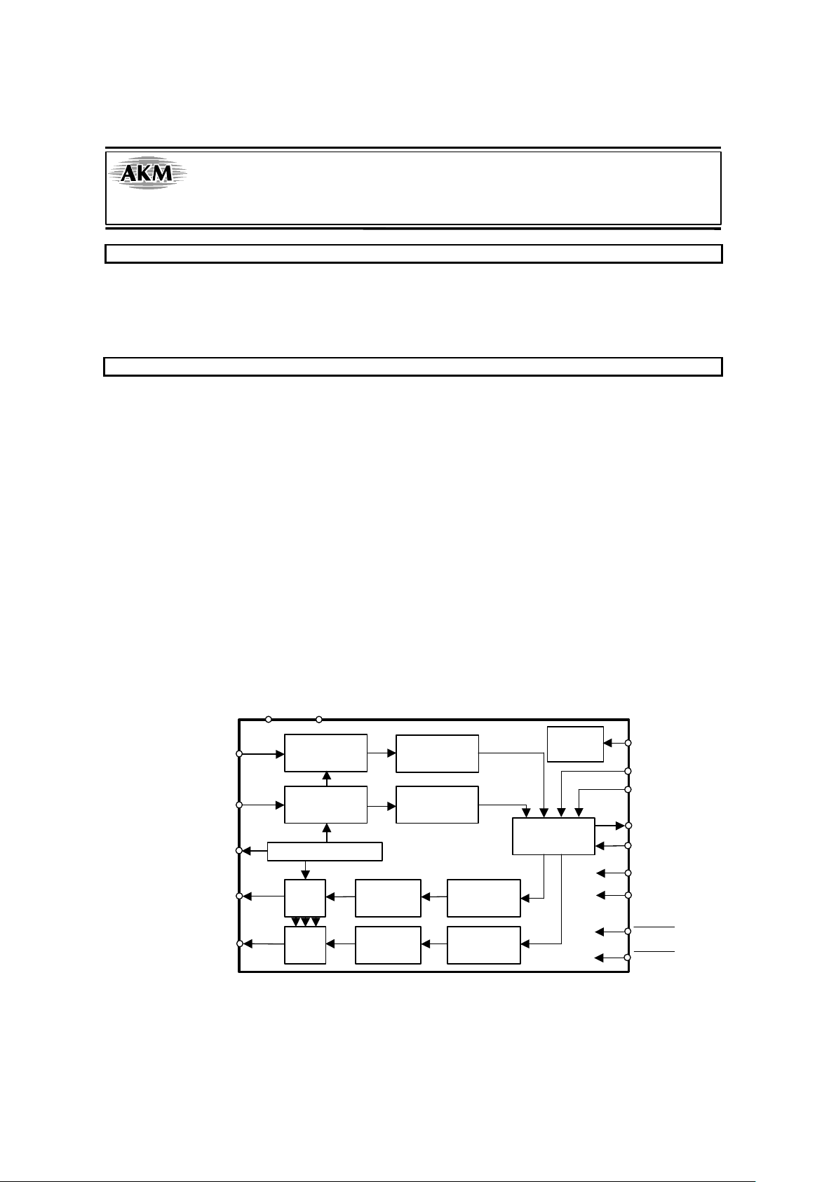
Modulator
MCLK
VDD
VSS
AOUTL
AINL
LRCK
SCLK
VCOM
AINR
∆Σ
Modulator
Decimation
Filter
Serial I/O
Interface
Common Voltage
SDTO
∆Σ
Decimation
Filter
SDTI
PWDA
DEM0
PWAD
Clock
Divider
AOUTR
8X
Interpolator
8X
Interpolator
∆Σ
Modulator
∆Σ
Modulator
LPF
LPF
DEM1
Low Power & Small Package 16bit ∆Σ CODEC
AK4550
ASAHI KASEI [AK4550]
M0068-E-01 2000/4
- 2 -
n Ordering Guide
AK4550VT -40 ∼ +85°C 16pin TSSOP (0.65mm pitch)
AKD4550 Evaluation Board for AK4550
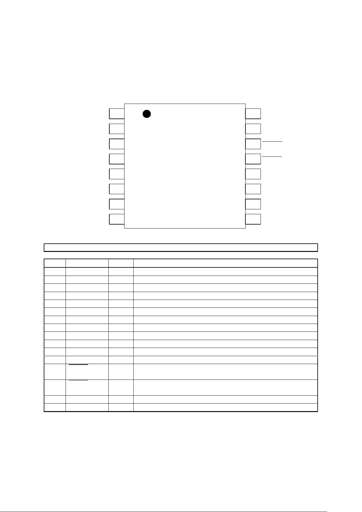
n Pin Layout
1VCOM
AINR
VSS
AINL
VDD
DEM0
DEM1
SDTO
Top
View
2
3
4
5
6
7
8
AOUTR
AOUTL
PWAD
SCLK
MCLK
LRCK
SDTI
16
15
14
13
12
11
10
9
PWDA
PIN/FUNCTION
No. Pin Name I/O Function
1 VCOM O Common Voltage Output Pin, 0.45 x VDD
2 AINR I Rch Analog Input Pin
3 AINL I Lch Analog Input Pin
4 VSS - Ground Pin
5 VDD - Power Supply Pin
6 DEM0 I De-emphasis Control Pin
7 DEM1 I De-emphasis Control Pin
8 SDTO O Audio Serial Data Output Pin
9 SDTI I Audio Serial Data Input Pin
10 LRCK I Input/Output Channel Clock Pin
11 MCLK I Master Clock Input Pin
12 SCLK I Audio Serial Data Clock Pin
13 PWAD I ADC Power-Down & Reset Mode Pin
“L”: Power down. ADC should always be reset upon power-up.
14 PWDA I DAC Power-Down & Reset Mode Pin
“L”: Power down. DAC should always be reset upon power-up.
15 AOUTL O Lch Analog Output Pin
16 AOUTR O Rch Analog Output Pin
ASAHI KASEI [AK4550]
M0068-E-01 2000/4
- 3 -
ABSOLUTE MAXIMUM RATINGS
(VSS=0V; Note 1)
Parameter Symbol min max Units
Power Supply VDD -0.3 4.6 V
Input Current (Any Pin Except Supplies) IIN -
±10
mA
Input Voltage VIN -0.3 VDD+0.3 V
Ambient Temperature (power applied) Ta -40 85
°C
Storage Temperature Tstg -65 150
°C
Note:1. All voltages with respect to ground.
WARNING: Operation at or beyond these limits may results in permanent damage to the device.
Normal operation is not guaranteed at these extremes.
RECOMMENDED OPERATING CONDITIONS
(VSS=0V; Note 1)
Parameter Symbol min typ max Units
Power Supply VDD 2.3 2.5 3.6 V
Note:1. All voltages with respect to ground.
*AKM assumes no responsibility for the usage beyond the conditions in this data sheet.
ASAHI KASEI [AK4550]
M0068-E-01 2000/4
- 4 -
ANALOG CHARACTERISTICS
(Ta=25°C; VDD=2.5V; fs=44.1kHz; Signal Frequency=1kHz ; SCLK=64fs; Measurement frequency=10Hz ∼ 20kHz;
unless otherwise specified)
Parameter min typ max Units
ADC Analog Input Characteristics: Analog Source Impedance=470Ω (Note 2)
Resolution 16 Bits
S/(N+D) (-0.5dB Input) 72 82 dB
D-Range (-60dB Input, A-weighted) 82 89 dB
S/N (A-weighted) 82 89 dB
Interchannel Isolation 80 95 dB
Interchannel Gain Mismatch 0.2 0.5 dB
Input Voltage (Note 3) 1.35 1.50 1.65 Vpp
Input Resistance 50 100
kΩ
Power Supply Rejection (Note 4) 35 dB
DAC Analog Output Characteristics: (Note 5)
Resolution 16 Bits
S/(N+D) 75 85 dB
D-Range (-60dB Output, A-weighted) 86 92 dB
S/N (A-weighted) 86 92 dB
Interchannel Isolation 80 95 dB
Interchannel Gain Mismatch 0.2 0.5 dB
Output Voltage (Note 3) 1.35 1.50 1.65 Vpp
Load Resistance 10
kΩ
Load Capacitance 30 pF
Power Supply Rejection (Note 4) 50 dB
Power Supplies
Power Supply Current
AD+DA
AD
DA
Power down (Note 6)
PWAD
= “H”, PWDA = “H”
PWAD
= “H”, PWDA = “L”
PWAD
= “L”, PWDA = “H”
PWAD
= “L”, PWDA = “L”
10
5.6
5.6
10
15
8.4
8.4
50
mA
mA
mA
uA
Power Consumption
AD+DA
AD
DA
Power down (Note 6)
PWAD
= “H”, PWDA = “H”
PWAD
= “H”, PWDA = “L”
PWAD
= “L”, PWDA = “H”
PWAD
= “L”, PWDA = “L”
25
14
14
25
37.5
21
21
125
mW
mW
mW
uW
Notes: 2. The offset of ADC is removed by internal HPF.
3. Input /Output of ADC and DAC scales with VDD voltage. 0.6 X VDD(typ).
4. PSR is applied to VDD with 1kHz, 50mV.
5. Measured by AD725C (SHIBASOKU). RMS mode.
6. In case of power-down mode, all digital input including clocks pins (MCLK, SCLK, LRCK) are held VDD
or VSS. But PWAD
and PWDA pins are held VSS.

ASAHI KASEI [AK4550]
M0068-E-01 2000/4
- 5 -
FILTER CHARACTERISTICS
(Ta=25°C; VDD=2.3 ∼ 3.6V; fs=44.1kHz; DEM0=”1”, DEM1=”0”)
Parameter Symbol min typ max Units
ADC Digital Filter (Decimation LPF):
Passband (Note 7)
±0.1dB
-1.0dB
-3.0dB
PB 0
20.0
21.1
17.4 kHz
kHz
kHz
Stopband SB 27.0 kHz
Passband Ripple PR
±0.1
dB
Stopband Attenuation SA 65 dB
Group Delay (Note 8) GD 17.0 1/fs
Group Delay Distortion
∆GD
0us
ADC Digital Filter (HPF):
Frequency Response (Note 7) -3dB
-0.5dB
-0.1dB
FR 3.4
10
22
Hz
Hz
Hz
DAC Digital Filter:
Passband (Note 7)
±0.1dB
-6.0dB
PB 0
22.05
20.0 kHz
kHz
Stopband SB 24.1 kHz
Passband Ripple PR
±0.06
dB
Stopband Attenuation SA 43 dB
Group Delay (Note 8) GD 14.8 1/fs
DAC Digital Filter + Analog Filter
Frequency Response 0 ∼ 20.0kHz
FR
±0.5
dB
Notes: 7. The passband and stopband frequencies scale with fs (sampling frequency).
For examples, PB=20.0kHz(@ADC: -1.0dB, DAC: -0.1dB) are 0.454 x fs.
8. The calculating delay time which occurred by digital filtering. This time is from the input of analog signal to
setting the 16bit data of both channels to the output register for ADC. For DAC, this time is from setting the
16bit data of both channels on input register to the output of analog signal.
DC CHARACTERISTICS
(Ta=25°C; VDD=2.3 ∼ 3.6V)
Parameter Symbol min typ max Units
High-Level Input Voltage
Low-Level Input Voltage
VIH
VIL
70%VDD
-
-
-
-
30%VDD
V
V
High-Level Output Voltage (Iout=-20uA)
Low-Level Output Voltage (Iout=20uA)
VOH
VOL
VDD-0.1
-
--
0.1
V
V
Input Leakage Current Iin - -
± 10
uA

ASAHI KASEI [AK4550]
M0068-E-01 2000/4
- 6 -
SWITCHING CHARACTERISTICS
(Ta=25°C; VDD=2.3 ∼ 3.6V; CL=20pF)
Parameter Symbol min typ max Units
Master Clock Timing 256fs:
Pulse Width Low
Pulse Width High
384fs:
Pulse Width Low
Pulse Width High
512fs:
Pulse Width Low
Pulse Width High
fCLK
tCLKL
tCLKH
fCLK
tCLKL
tCLKH
fCLK
tCLKL
tCLKH
2.048
28
28
3.072
23
23
4.096
16
16
11.2896
16.9344
22.5792
12.8
19.2
25.6
MHz
ns
ns
MHz
ns
ns
MHz
ns
ns
LRCK Frequency
Duty Cycle
fs 8
45
44.1 50
55
kHz
%
Serial Interface Timing
SCLK Period
SCLK Pulse Width Low
Pulse Width High
LRCK Edge to SCLK “↑” (Note 9)
SCLK “↑” to LRCK Edge (Note 9)
LRCK Edge to SDTO (MSB)
SCLK “↓” to SDTO
SDTI Hold Time
SDTI Setup Time
tSCK
tSCKL
tSCKH
tLRS
tSLR
tDLR
tDSS
tSDH
tSDS
312.5
130
130
50
50
50
50
80
80
ns
ns
ns
ns
ns
ns
ns
ns
ns
Reset Timing
PWAD
or PWDA Pulse Width
PWAD
”↑” to SDTO Valid (Note 10)
tPW
tPWV
150
2081
ns
1/fs
Notes: 9. SCLK rising edge must not occur at the same time as LRCK edge.
10. These cycles are the number of LRCK rising from PWAD
rising.

ASAHI KASEI [AK4550]
M0068-E-01 2000/4
- 7 -
n Timing Diagram
LRCK
SCLK
50%
VDD
SDTO
tSLR tLRS
tDLR tDSS
tSCKLtSCKH
SDTI
50%
VDD
50%
VDD
50%
VDD
tSDHtSDS
Serial Interface Timing
tPW
PWDA
SDTO
tPWV
50%VDD
PWAD
50%VDD
tPW
Reset & Initialize Timing

ASAHI KASEI [AK4550]
M0068-E-01 2000/4
- 8 -
OPERATION OVERVIEW
n System Clock Input
The AK4550 can be input MCLK=256fs, 384fs or 512fs. The input clock applied to the MCLK as internal master clock
is divided into 256fs automatically. The relationship between the external clock applied to the MCLK input and the
desired sample rate is defined in Table 1. The LRCK clock input must be synchronized with MCLK, however the phase
is not critical. *fs is sampling frequency.
When the synchronization is out of phase by changing the clock frequencies during normal operation, the AK4550 may
occur click noise. In case of DAC, click noise is avoided by setting the inputs to “0”.
All external clocks(MCLK, SCLK, LRCK) must be present unless PWAD
and PWDA = ”L”. If these clocks are not
provided, the AK4550 may draw excess current and may not possibly operate properly because the device utilizes
dynamic refreshed logic internally.
MCLK SCLK
fs
256fs 384fs 512fs 32fs 64fs
32.0kHz 8.1920MHz 12.2880MHz 16.3840MHz 1.0240MHz 2.048MHz
44.1kHz 11.2896MHz 16.9344MHz 22.5792MHz 1.4112MHz 2.822MHz
48.0kHz 12.2880MHz 18.4320MHz 24.5760MHz 1.5360MHz 3.072MHz
Table 1. System Clock Example
n Audio Serial Interface Format
Data is shifted in/out the SDTI/SDTO pins using SCLK and LRCK inputs. The data is MSB first, 2’s compliment.
SDTI(i)
SCLK(i)
LRCK
SDTI(i)
SCLK(i)
0 1 10 11 12 13 14 15 0 1 10 11 12 13 14 15 0 1
(32fs)
(64fs)
014
1
15 16 17 31 0 1
14
15 16 17 31 0 1
15:MSB, 0:LSB
Lch Data Rch Data
15 14 6 5 4 3 2 1 0 15 141514 6543210
15 14 0
15 14 0
Don’t care
Don’t care
SDTO(o)
15 14
2
1 0 15 14
15 14 2 1 0
SDTO(o)
Figure 1. Audio Interface Timing

ASAHI KASEI [AK4550]
M0068-E-01 2000/4
- 9 -
n De-emphasis filter
The DAC of AK4550 includes the digital de-emphasis filter (tc=50/15us) by IIR filter. This filter corresponds to three
frequencies (32kHz, 44.1kHz, 48kHz). The de-emphasis filter selected by DEM0 and DEM1 is enabled for input audio
data. The de-emphasis is also disabled at DEM0=”1” and DEM1=”0”.
DEM1 DEM0 Mode
0 0 44.1kHz
0 1 OFF
1 0 48kHz
1 1 32kHz
Table 2. De-emphasis filter control
n Digital High Pass Filter
The AK4550 has a Digital High Pass Filter (HPF) for DC-offset cancel. The cut-off frequency of the HPF is 3.4Hz at
fs=44.1kHz and the frequency response at 20Hz is –0.12dB. It also scales with the sampling frequency (fs).

ASAHI KASEI [AK4550]
M0068-E-01 2000/4
- 10 -
n Power-down & Reset
The ADC and DAC of AK4550 are placed in the power-down mode by bringing each power down pin, PWAD , PWDA
= “L” independently and each digital filter is also reset at the same time. These resets should always be done after
power-up. In case of the ADC, an anlog initialization cycle starts after exiting the power-down mode. Therefore, the
output data, SDTO becomes available after 2081 cycles of LRCK clock. This initialization cycle does not affect the DAC
operation. Figure 2 shows the power-up sequence when the ADC is powered up before the DAC power-up.
Idle Noise
The clocks may be stopped.
ADC Internal
State
PWAD
2081/fs
Normal Operation Power-down Init Cycle Normal Operation
GD
GD
Clock In
MCLK,LRCK,SCLK
ADC In
(Analog)
Idle Noise
“0”data
ADC Out
(Digital)
PWDA
Normal Operation
Power-down
Normal Operation
DAC Internal
State
“0”data
DAC In
(Digital)
DAC Out
(Analog)
GD
External
Mute
Mute ON
GD
Figure 2. Power-up Sequence

ASAHI KASEI [AK4550]
M0068-E-01 2000/4
- 11 -
SYSTEM DESIGN
Figure 3 shows the system connection diagram. An evaluation board[AKD4550] is available which demonstrates
application circuit, optimum layout, power supply arrangements and measurement results.
VCOM1
AINR2
AINL3
VSS4
VDD5
DEM06
DEM17
SDTO8
16
15
14
13
12
11
10
9
AOUTR
AOUTL
PWAD
SCLK
MCLK
LRCK
SDTI
AK4550
Top View
0.1u
2.2n
470
2.2n
470
+
+
Rch In
Lch In
Analog Supply
10u
+
Controller
System GroundAnalog Ground
PWDA
Reset
Reset
+
0.1u4.7u
Mode
Control
2.3 ∼ 3.6V
Figure 3. System Connection Diagram Example
Notes:
- LRCK=fs, 32fs ≤ SCLK ≤ 96fs, MCLK=256fs/384fs/512fs.
- When AOUT drives some capacitive load, some resistor should be added in series between AOUT and capacitive
load.
- Electrolytic capacitor value of VCOM depends on low frequency noise of supply voltage.

ASAHI KASEI [AK4550]
M0068-E-01 2000/4
- 12 -
1. Grounding and Power Supply Decoupling
VDD and VSS are supplied from analog supply and should be separated from system digital supply. Decoupling
capacitors should be as near to the AK4550 as possible, with the small value ceramic capacitor being nearest.
2. Voltage Reference
The input to VDD voltage sets the analog input/output range. A 0.1uF ceramic capacitor and a 10uF electrolytic capacitor
is connected to VDD and VSS pins, normally. VCOM is a signal ground of this chip. An electrolytic less than 4.7uF in
parallel with a 0.1uF ceramic capacitor attached to these pins eliminates the effects of high frequency noise. No load
current may be drawn from VCOM pin. All signals, especially clock, should be kept away from the VDD, VCOM pins in
order to avoid unwanted coupling into the AK4550.
3. Analog Inputs
ADC inputs are single-ended and internally biased to VCOM. The input signal range scales with the supply voltage and
nominally 0.6xVDD Vpp(typ). The ADC output data format 2’s compliment. The output code is 7FFFH(@16bit) for
input above a positive full scale and 8000H(@16bit) for input below a negative full scale. The ideal code is
0000H(@16bit) with no input signal.
The AK4550 samples the analog inputs at 64fs. The digital filter rejects noise above the stop band except for multiples of
64fs. A simple RC filter (fc=150kHz) may be used to attenuate any noise around 64fs and most audio signals do not have
significant energy at 64fs.
4. Analog Outputs
The analog outputs are also single-ended and centered around the VCOM voltage. The input signal range scales with the
supply voltage and nominally 0.6xVDD Vpp(typ). The DAC input data format is 2’s compliment. The output voltage is
a positive full scale for 7FFFH(@16bit) and a negative full scale for 8000H(@16bit). The ideal output is VCOM voltage
for 0000H(@16bit). If the noise generated by the delta-sigma modulator beyond the audio band would be the problem, the
attenuation by external filter is required.
DC offsets on analog outputs are eliminated by AC coupling since DAC outputs have DC offsets of a few mV.

ASAHI KASEI [AK4550]
M0068-E-01 2000/4
- 13 -
n Layout Pattern Example
AK4550 requires careful attention to power supply and grounding arrangements to optimize performance.
(Please refer to AKD4550 Evaluation Board layout pattern.)
1. VDD pin should be supplied from analog power supply on system, and VSS pin should be connected to analog
ground on system. The AK4550 is placed on the analog ground plane, and near the analog ground and digital
ground split. And analog and digital ground planes should be only connected at one point. The connection point
should be near to the AK4550.
2. VDD pin should be distributed from the point with low impedance of regulator etc.
3. The series resistors are prevent on the clock lines to reduce overshoot and undershoot. To avoid digital noise
coupling to analog circuit in the AK4550, a 10pF ceramic capacitor on MCLK pin is connected with digital ground.
4. 0.1uF ceramic capacitors of VDD-VSS pins and VCOM-VSS pins should be located as close to the AK4550 as
possible. And these lines should be the shortest connection to pins.
0.1u
2.2n
470
2.2n
470
Rch In
Lch In
Analog Supply
10u
Controller
Digital Ground
Analog Ground
0.1u4.7u
2.3 ∼ 3.6V
VCOM
AINR
2
AINL
VSS
VDD
5
DEM0
6
DEM1
7
SDTO
1
0
9
AOUTR
AOUTL
PWAD
SCL
K
MCLK
LRCK
SDTI
AK4550
Top View
PWDA
10P
Reset &Power-down
Mode Control
51
51
51
51
51
Figure 4. Layout Pattern Example

ASAHI KASEI [AK4550]
M0068-E-01 2000/4
- 14 -
PACKAGE
0.1±0.1
0-10
°
Detail A
Seating Plane
NOTE: Dimension "*" does not include mold flash.
0.10
0.17±0.05
0.22±0.1 0.65
*5.0 1.10max
A
1
8
916
16pin TSSOP (Unit: mm
)
*4.4
6.4
±
0.2
0.5
±
0.2
1.0
n Package & Lead frame material
Package molding compound: Epoxy
Lead frame material: Cu
Lead frame surface treatment: Solder plate

ASAHI KASEI [AK4550]
M0068-E-01 2000/4
- 15 -
MARKING
AKM
4550VT
XXYYY
1) Pin #1 indication
2) Date Code : XXYYY (5 digits)
XX: lot#
YYY: Date Code
3) Marketing Code : 4550VT
4) Asahi Kasei Logo
IMPORTANT NOTICE
• These products and their specifications are subject to change without notice. Before considering any use or
application, consult the Asahi Kasei Microsystems Co., Ltd. (AKM) sales office or authorized distributor
concerning their current status.
• AKM assumes no liability for infringement of any patent, intellectual property, or other right in the
application or use of any information contained herein.
• Any export of these products, or devices or systems containing them, may require an export license or other
official approval under the law and regulations of the country of export pertaining to customs and tariffs,
currency exchange, or strategic materials.
• AKM products are neither intended nor authorized for use as critical components in any safety, life support,
or other hazard related device or system, and AKM assumes no responsibility relating to any such use,
except with the express written consent of the Representative Director of AKM. As used here:
a. A hazard related device or system is one designed or intended for life support or maintenance of safety
or for applications in medicine, aerospace, nuclear energy, or other fields, in which its failure to
function or perform may reasonably be expected to result in loss of life or in significant injury or
damage to person or property.
b. A critical component is one whose failure to function or perform may reasonably be expected to result,
whether directly or indirectly, in the loss of the safety or effectiveness of the device or system
containing it, and which must therefore meet very high standards of performance and reliability.
• It is the responsibility of the buyer or distributor of an AKM product who distributes, disposes of, or
otherwise places the product with a third party to notify that party in advance of the above content and
conditions, and the buyer or distributor agrees to assume any and all responsibility and liability for and hold
AKM harmless from any and all claims arising from the use of said product in the absence of such
notification.
 Loading...