


[AK4635]
= Preliminary =
AK4635
The AK4635 is a 16-bit mono CODEC with Microphone-Amplifier, Speaker-Amplifier and VideoAmplifier. Input circuits include a Microphone-Amplifier and an ALC (Automatic Level Control) circuit.
Output circuits include a Speaker-Amplifier and Mono Line Output. Video circuits include a LPF and
Video-Amplifier. The AK4635 suits a moving picture of Digital Still Camera and etc. This
speaker-Amplifier supports a Piezo Speaker. The AK4635 is housed in a space-saving 29-pin Wafer
Level CSP 2.5mm x 3.0mm package.
16-Bit Mono CODEC with ALC & MIC/SPK/Video-AMP
GENERAL DESCRIPTION
FEATURE
1. 16-Bit Delta-Sigma Mono CODEC
2. Recording Function
• 1ch Mono Input
• MIC Amplifier: (0dB/+3dB/+6dB/+10dB/ +17dB/+20dB/+23dB/+26dB/+29dB/+32dB)
• Digital ALC (Automatic Level Control)
(+36dB ∼ -54dB, 0.375dB Step, Mute)
• ADC Performance (MIC-Amp=+20dB)
- S/(N+D): 84dB
- DR, S/N: 86dB
• Wind-noise Reduction Emphasis
• 5 band notch Filter
3. Playback Function
• Digital ALC (Automatic Level Control)
(+36dB ∼ -54dB, 0.375dB Step, Mute)
• Mono Line Output: S/(N+D) : 85dB, S/N : 93dB
• Mono Class-D Speaker-Amp
- BTL Output
- Output Power: 400mW @ 8Ω (SVDD=3.3V)
- S/(N+D): 55dB (150mW@8Ω)
• Beep Generator
4. Video Function
• A Composite Video Input
• Gain Control (-1.0dB ∼ +10.5dB, 0.5dB Step)
• Low Pass Filter
• A Video-Amp for Composite Video Signal(+6dB)
• DC Direct Output or Sag Compensation Output
5. Power Management
6. PLL Mode:
• Frequencies:
12MHz, 13.5MHz, 24MHz, 27MHz (MCKI pin)
1fs (FCK pin)
16fs, 32fs or 64fs (BICK pin)
7. EXT Mode:
• Frequencies: 256fs, 512fs or 1024fs (MCKI pin)
8. Sampling Rate:
• PLL Slave Mode (FCK pin): 7.35kHz
• PLL Slave Mode (BICK pin): 7.35kHz
• PLL Slave Mode (MCKI pin):
~ 48kHz
~ 48kHz
Rev. 0.6 2007/10
- 1 -

[AK4635]
8kHz, 11.025kHz, 12kHz, 16kHz, 22.05kHz, 24kHz, 32kHz, 44.1kHz, 48kHz
• PLL Master Mode:
8kHz, 11.025kHz, 12kHz, 16kHz, 22.05kHz, 24kHz, 32kHz, 44.1kHz, 48kHz
• EXT Slave Mode / EXT Master Mode:
7.35kHz
9. Output Master Clock Frequency: 256fs
10. Serial μP Interface: 3-wire, I
~ 48kHz (256fs), 7.35kHz ~ 26kHz (512fs), 7.35kHz ~ 13kHz (1024fs)
2
C Bus (Ver 1.0, 400kHz High Speed Mode)
11. Master / Slave Mode
12. Audio Interface Format: MSB First, 2’s compliment
• ADC: DSP Mode, 16bit MSB justified, I
• DAC: DSP Mode, 16bit MSB justified, 16bit LSB justified, I
2
S
2
S
13. Ta = - 30 ∼ 85°C
14. Power Supply
• Analog Supply (AVDD): 2.8 ∼ 3.6V
• Digital Supply (DVDD): 1.6 ∼ 3.6V
• Speaker Supply (SVDD): 2.2 ∼ 4.0V
15. Package: 29pin CSP (2.5mm x 3.0mm, 0.5mm pitch)
■ Block Diagram
MPI
PMMP
MIC Power
AVDD VSS1 VCOM DVDD
Supply
VSS2
PDN
I2C
Line Out
Speaker
Mic
Composite
Video Out
MIC/MICP
LIN/MICN
AOUT
SVDD
VSS3
SPP
SPN
VOUT
VSAG
PMADC
MIC-Amp
0dB /+3dB/+6dB/+10dB/+17dB/+20dB
+23dB+26dB / +29dB / +32dB
PMAO
PMSPK
Class-D
SPK-AMP
PMV
+6dB
-1dB ~ +10.5dB
Step 0.5dB
Figure 1. AK4635 Block Diagram
A/D
PMDAC
&
PMAO
D/A
GCA LPF
HPF
VIN
CLAMP
PMDAC
SMUTE
PMSPK
Generator
BEEP
DATT
PMPFIL
HPF
LPF
5 Band
EQ
VOL
(ALC)
Audio
I/F
PMPLL
PLL
Control
Register
BICK
FCK
SDTO
SDTI
MCKO
MCKI
VCOC
CSN/SDA
CCLK/SCL
CDTIO
Rev. 0.6 2007/10
- 2 -

[AK4635]
■ Ordering Guide
AK4635ECB −30 ∼ +85°C 29pin CSP (0.5mm pitch)
AKD4635 Evaluation board for AK4635
■ Pin Layout
6
5
4
Top View
3
2
1
A BC ED
6 I2C DVDD VSS2 VSS3 NC
5 SDTO MCKO SPN SVDD SPP
4 BICK SDTI MCKI AOUT
3 FCK CCLK/SCL CDTIO MPI
2 PDN CSN/SDA VOUT VCOM VCOC
1 VSAG VSS1 AVDD VIN
A B C D E
LIN/
MICN
MIC/
MICP
Rev. 0.6 2007/10
- 3 -

[AK4635]
■ Compatibility with AK4633
1. Function
Function AK4633 AK4635
MIC-Amp 0dB/+6dB/+10dB/+14dB
+17dB/+20dB/+26dB/+32dB
Single End of Analog Input 1ch (MIC pin) 2ch (MIC pin / LIN pin)
LPF Not Available Available
Notch Filter ( Equalizer) 2 band 5 band
SPK-Amp Class-AB Class-D
ALC Recovery Waiting Period 4 steps
(128fs ~ 1024fs)
Master Clock Mode
PLL Mode Frequency
BEEP Output Analog Input Generator circuit Included
Control Interface 3-wire 3-wire, I2C
Video-Amp Not Available Available
Package 24pin QFN: 4.0mm x 4.0mm 29pin WL-CSP : 2.5mm x 3.0mm
11.2896MHz, 12MHz,
12.288MHz, 13.5MHz
24MHz, 27MHz
0dB/+3dB/+6dB/+10dB/+17dB/
+20dB/+23dB/+26dB/+29dB/
+32dB
8 steps
(128fs ~ 16384fs)
12MHz, 13.5MHz, 24MHz,
27MHz
Rev. 0.6 2007/10
- 4 -

[AK4635]
PIN/FUNCTION
No. Pin Name I/O Function
D2 VCOM O
C1
VSS1 - Ground Pin
D1
AVDD - Analog Power Supply Pin
E2
VCOC O
Common Voltage Output Pin, 0.45 x AVDD
Bias voltage of ADC inputs and DAC outputs.
Output Pin for Loop Filter of PLL Circuit
This pin should be connected to VSS1 with one resistor and capacitor in series.
Power-Down Mode Pin
A2
PDN I
“H”: Power up, “L”: Power down reset and initialize the control register.
AK4635 should always be reset when powered-up.
A6 I2C I
CSN I Chip Select Pin (I2C pin = “L”)
B2
SDA I/O Control Data Input/Output Pin (I2C pin = “H”)
CCLK I Control Data Clock Pin (I2C pin = “L”)
B3
SCL I Control Data Clock Pin (I2C pin = “H”)
C3 CDTIO I/O
B4
SDTI I Audio Serial Data Input Pin
A5
SDTO O Audio Serial Data Output Pin
A3
FCK I/O Frame Clock Pin
A4
BICK I/O Audio Serial Data Clock Pin
B6
DVDD - Digital Power Supply Pin
C6
VSS2 - Ground Pin
C4
MCKI I
B5
MCKO O Master Clock Output Pin
E5
SPP O Speaker Amp Positive Output Pin
C5
SPN O Speaker Amp Negative Output Pin
D6
VSS3 - Ground Pin
D5
SVDD - Speaker Amp Power Supply Pin
D4
AOUT O Mono Line Output Pin
D3
MPI O MIC Power Supply Pin for Microphone
MIC I Microphone Input Pin for Single Ended Input (MDIF bit = “0”)
E3
Control Mode Select Pin
2
C Bus, “L”:3-wire Serial
“H”:I
Control Data Input/Output Pin (I2C pin = “L”)
This pin should be connected to the ground. (I2C pin = “H”)
External Master Clock Input Pin
MICP I Microphone Positive Input Pin for Differential Input (MDIF bit = “1”)
LIN I Line Input Pin for Single Ended Input (MDIF bit = “0”)
E4
MICN I Microphone Negative Input Pin for Differential Input (MDIF bit = “1”)
E1
VIN I Composite Video Signal Input Pin
C2
VOUT O Composite Video Signal Driver Pin
A1
VSAG I Composite Video Signal Output Feedback Input Pin
E6
NC -
No Connection
No internal bonding. This pin should be connected to the ground.
Note : All input pins except analog input pins (MIC/MICP, LIN/MICN, VIN, VSAG pins) must not be left floating
Rev. 0.6 2007/10
- 5 -

[AK4635]
■ Handling of Unused Pin
The unused I/O pins should be processed appropriately as below.
Classification Pin Name Setting
Analog
Digital
MIC/MICP, LIN/MICN, MPI, AOUT,
SPP, SPN, VCOC, VIN, VOUT, VSAG
MCKI, SDTI These pins should be connected to VSS2
CDTIO
MCKO, SDTO These pins should be open.
ABSOLUTE MAXIMUM RATINGS
(VSS1-3 =0V; Note 1)
Parameter Symbol min max Units
Power Supplies:
Input Current, Any Pin Except Supplies IIN - ±10 mA
Analog Input Voltage (Note 3) VINA −0.3 AVDD+0.3 V
Digital Input Voltage (Note 4) VIND −0.3 DVDD+0.3 V
Ambient Temperature (powered applied) Ta −40 85 °C
Storage Temperature Tstg −65 150 °C
Maximum Power Dissipation (Note 2) Pd - 400 mW
Note 1. All voltages with respect to ground. VSS21, VSS2 and VSS3 must be connected to the same analog ground plane.
Note 2.When PCB wiring density is 100%. This power is the AK4635 internal dissipation that does not include power of
externally connected speaker.
Note 3. LIN/MICN, MIC/MICP,VIN pins
Note 4. PDN, I2C, CSN/SDA, CCLK/SCL, CDTIO, SDTI, FCK, BICK, MCKI pins
Pull-up resistors at SDA and SCL pins should be connected to (DVDD+0.3)V or less voltage.
WARNING: Operation at or beyond these limits may result in permanent damage to the device.
Normal operation is not guaranteed at these extremes.
Analog
Digital
Speaker-Amp
AVDD
DVDD
SVDD
RECOMMENDED OPERATING CONDITIONS
(VSS1-3=0V; Note 1)
Parameter Symbol Min typ max Units
Power Supplies
(
Note 5)
Note 1. All voltages with respect to ground.
Note 5. The power up sequence between AVDD, DVDD and SVDD is not critical. It is not permitted to power DVDD off
when AVDD or SVDD is powered up. When only AVDD or SVDD is powered OFF, the AK4635 must be reset
by bringing the PDN pin “L” after theses power supplies are powered ON again. The power supply current of
DVDD at power-down mode may be increased. DVDD should not be powered OFF while AVDD or SVDD is
powered ON.
Note 6. Video Amp is used (PMV bit = “1”). When Video Amp is not used (PMV bit = “0”), Min. spec of AVDD is 2.2V.
* AKEMD assumes no responsibility for the usage beyond the conditions in this datasheet.
Analog
Digital
Speaker-Amp
AVDD
DVDD
SVDD
2.8 (
These pins should be open
When I2C pin = “H”, These pins should be
connected to VSS2.
−0.3
−0.3
−0.3
Note 6)
1.6
2.2
3.3
3.3
3.3
4.6
4.6
4.6
3.6
3.6
4.0
V
V
V
V
V
V
Rev. 0.6 2007/10
- 6 -

[AK4635]
ANALOG CHRACTERISTICS
(Ta=25°C; AVDD=DVDD=SVDD=3.3V; VSS1-3 =0V; fs=8kHz, BICK=64fs; Signal Frequency=1kHz; 16bit Data;
Measurement frequency=20Hz ∼ 3.4kHz; EXT Slave Mode; unless otherwise specified)
Parameter min typ max Units
MIC Amplifier: MIC, LIN pins ; MDIF bit = “0”; (Single-ended input)
Input Resistance 20 30 40
Gain (MGAIN3-0 bits = “0000”) - 0 - dB
(MGAIN3-0 bits = “0001”) - 20 - dB
(MGAIN3-0 bits = “0010”) - 26 - dB
(MGAIN3-0 bits = “0011”) - 32 - dB
(MGAIN3-0 bits = “0100”) - 10 - dB
(MGAIN3-0 bits = “0101”) - 17 - dB
(MGAIN3-0 bits = “0110”) - 23 - dB
(MGAIN3-0 bits = “0111”) - 29 - dB
(MGAIN3-0 bits = “1000”) - 3 - dB
(MGAIN3-0 bits = “1001”) - 6 - dB
MIC Amplifier: MICP, MICN pins ; MDIF bit = “1”; (Full-differential input)
Input Voltage (MGAIN3-0 bits = “0001”) - - 0.228 Vpp
(Note 7) (MGAIN3-0 bits = “0010”) - - 0.114 Vpp
MIC Power Supply: MPI pin
Output Voltage (Note 8) TBD 2.64 TBD V
Load Resistance 2 - Load Capacitance - - 30 pF
ADC Analog Input Characteristics: MIC/LIN Æ ADC, MIC Gain=20dB, IVOL=0dB, ALC1bit = “0”
Resolution - - 16 Bits
Input Voltage (MIC Gain = 20dB) (Note 9) TBD 0.198 TBD Vpp
S/(N+D) (−1dBFS) (Note 10)
D-Range (−60dBFS)
S/N TBD 86 - dB
DAC Characteristics:
Resolution 16 Bits
Mono Line Output Characteristics: AOUT pin, DAC → AOUT, RL=10kΩ
Output Voltage (Note 11) LOVL bit = “0”
LOVL bit = “1”
S/(N+D) (0dBFS) (Note 10)
D-Range (-60dBFS)
S/N
Load Resistance
Load Capacitance
Speaker-Amp Characteristics: SDTI Æ SPP/SPN pins, ALC2 bit = “0”, SPKG bit = “0”, RL=8Ω + 10μH,
Output Power (0dBFS) (Note 12) - 400 - mW
S/(N+D) 400mW Output - 20 - dB
150mW Output - 55 - dB
Output Noise Level
Load Resistance 8 - Load Capacitance
(MGAIN3-0 bits = “0011”) - - 0.057 Vpp
(MGAIN3-0 bits = “0100”) - - 0.720 Vpp
(MGAIN3-0 bits = “0101”) - - 0.322 Vpp
(MGAIN3-0 bits = “0110”) - - 0.161 Vpp
(MGAIN3-0 bits = “0111”) 0.080 Vpp
(MGAIN3-0 bits = “1001”) - - 1.14 Vpp
TBD 84 - dB
TBD 86 - dB
TBD 1.98 TBD Vpp
TBD 2.50 TBD Vpp
TBD 85 - dB
TBD 93 - dB
TBD 93 - dB
10 - -
- - 30 pF
BTL, SVDD=3.3V
TBD -80 - dBV
- - 30 pF
kΩ
kΩ
kΩ
Ω
Rev. 0.6 2007/10
- 7 -

[AK4635]
Parameter Min Typ max Units
Speaker-Amp Characteristics: SDTI Æ SPP/SPN pins, ALC2 bit = “0”, SPKG bit = “0”, CL = 3μF, R
= 10Ω x 2,
series
BTL, SVDD = 3.8V
Output Voltage (0dBFS) (Note 12) - 2.5 - Vrms
S/(N+D) (Note 13) - 20 - dB
Output Noise Level (Note 13)
Load Impedance (Note 14) 50 - Load Capacitance
- -68 - dBV
Ω
- - 3
μF
V Input Characteristics:
Maximum Input Voltage (Note 17) - 1.2 - Vpp
Pull Down Current - 1.0 -
μA
V Output Characteristics:
Output Gain VIN = 100kHz (GCA = 0dB) (Note 18) TBD 6.0 TBD dB
Maximum Output at DC output TBD 2.52 - Vpp
Voltage
Note 18)
(
at Sag Compensation Output
at Sag Compensation Output
100μF+4.7μF, AVDD ≥ 3.0 V
47μF+4.7μF, AVDD ≥ 3.1V
- 2.4 - Vpp
- 2.4 - Vpp
Clamp Voltage at DC output (Note 18) - 50 - mV
S/N
BW = 100kH ∼ 6MHz (
Note 18)
Secondary Distortion VIN = 3.58MHz, 1.0Vpp (Sin Wave)
Note 18, Note 19)
(
Load Resistance 140 150 Load Capacitance CL1 (Figure 4)
2 (Figure 5)
C
L
3 (Figure 4, Figure 5) (Note 20)
C
L
LPF
Frequency Response
Input=1.26Vpp, Sin Wave
(0dB at 100kHz)
Group Delay
GCA Characteristics:
Step Size
Response at 6.75MHz
Response at 27MHz
|GD3MHz − GD6MHz|
GCA = −1.0dB ∼ +10.5dB
Power Supplies
- 66 - dB
- -45 - dB
Ω
-
-
-
-
-
-
30
15
400
pF
pF
pF
TBD -0.5 - dB
- -40 TBD dB
- 10 100 ns
TBD 0.5 TBD dB
Power Up (PDN pin = “H”)
All Circuit Power-up Except Video Amp (Note 21)
AVDD+DVDD
fs = 8kHz - 9 - mA
fs = 48kHz - 12 TBD mA
SVDD: Speaker-Amp Normal Operation (No Output)
SVDD=3.3V - 1.5 TBD mA
Video Amp Power-up : (Note 22) (Note 24)
AVDD+DVDD - 8 TBD mA
All Circuit Power-up : (Note 23) (Note 24)
AVDD+DVDD fs = 48kHz - 19 TBD mA
Power Down (PDN pin = “L”) (Note 25)
AVDD+DVDD+SVDD
- 1 TBD
μA
Note 7. The voltage difference between MICP and MICN pins. AC coupling capacitor should be inserted in series at each
input pin. Full-differential mic input is not available at MGAIN3-0 bits = “1000” or “0000”. Maximum input
voltage of MICP and MICN pins are proportional to AVDD voltage, respectively.
Vin = |(MICP) − (MICN)| = 0.069 x AVDD(max)@MGAIN3-0 bits = “0001”,
0.035 x AVDD(max)@MGAIN3-0 bits = “0010”, 0.017 x AVDD(max)@MGAIN3-0 bits = “0011”,
0.218x AVDD(max)@MGAIN3-0 bits = “0100”, 0.097x AVDD(max)@MGAIN3-0 bits = “0101”,
0.048x AVDD(max)@MGAIN3-0 bits = “0110”, 0.024x AVDD(max)@MGAIN3-0 bits = “0111”,
Rev. 0.6 2007/10
- 8 -

[AK4635]
0.345x AVDD(max)@MGAIN3-0 bits = “1001”
When the signal larger than above value is input to MICP or MICN pin, ADC does not operate normally.
Note 8. Output voltage is proportional to AVDD voltage. Vout = 0.8 x AVDD (typ)
Note 9. Input voltage is proportional to AVDD voltage. Vin = 0.06 x AVDD (typ)
Note 10. When a PLL reference clock is FCK pin in PLL Slave Mode, S/ (N+D) of MICÆADC is 75dB (typ), S/ (N+D)
of DACÆAOUT is 75dB (typ).
Note 11. Output voltage is proportional to AVDD voltage. Vout = 0.6 x AVDD (typ)@LOVL bit = “0”.
Note 12. The value after passing LPF (LPF : Passband is 20kHz or less, Stopband Attenuation@250kHz is –50dB or less)
Note 13. In case of measuring at between the SPP pin and SPN pin directly.
Note 14. Load impedance is total impedance of series resistance (R
) and piezo speaker impedance at 1kHz in
series
Figure 48. Load capacitance is capacitance of piezo speaker. When piezo speaker is used, 10Ω or more series
resistors should be connected at both SPP and SPN pins, respectively.
Note 15. Maximum input voltage is in proportion to both AVDD and external input resistance (Rin). Vin = 0.6 x AVDD
x Rin/20kΩ (typ).
Note 16. Output voltage is proportional to AVDD voltage. Vout = 0.6 x AVDD (typ).
Note 17. Input Voltage does not depend on AVDD voltage.
Note 18. Measurement point is A of
Figure 2 and Figure 3 when Sag Compensation mode and DC Output mode.
Measurement point A
VIN
CLAMP
LPF GCA
-1dB ~ +10.5dB
Step 0.5dB
+6dB
VOTU
VSAG
75Ω
Figure 2 Measurement Point (at DC Output)
VIN
CLAMP
LPF GCA
-1dB ~ +10.5dB
Step 0.5dB
+6dB
VOUT
VSAG
Measurement point A
C1
75Ω
C2
Figure 3. Measurement Point (Using Sag Compensation circuit)
Note 19. In the case of using Sag Compensation Circuit with 47μF+ 4.7μF and SAGC bit = “1”
Note 20. R1 and C2 compose of Low Pass Filter (LPF) in
Figure 5. The cut off frequency of LPF is 10.6MHz at
C2=400pF.
75Ω
75Ω
R1
VIN
CLAMP
LPF GCA
-1dB ~ +10.5dB
Step 0.5dB
+6dB
VOUT
VSAG
CL1
75Ω
R2
75Ω
CL3
Figure 4. Load Capacitance C
1 and CL3 (at DC Output)
L
Rev. 0.6 2007/10
- 9 -

[AK4635]
R1
C1
C2
CL2
75Ω
R2
75Ω
CL3
VIN
CLAMP
LPF GCA
-1dB ~ +10.5dB
Step 0.5dB
+6dB
VOUT
VSAG
CL2
CL2
Figure 5. Load Capacitance C
2 and CL3 (Using Sag Compensation circuit)
L
Note 21.PLL Master Mode (MCKI = 12MHz) and PMMP = PMADC = PMDAC = PMPFIL = PMSPK = PMVCM =
PMPLL = MCKO = PMAO = M/S = “1” and PMV bit = “0”. And output current from the MPI pin is 0mA.
When the AK4635 is EXT mode (PMPLL = MCKO = M/S = “0”), “AVDD+DVDD” is typically TBD
mA@fs=8kHz, TBDmA@fs=48kHz
Note 22. PMVCM = PMV bits = “1”, PMMP = PMADC = PMDAC = PMPFIL = PMSPK = PMPLL = MCKO = PMAO
= M/S =“0”. And output current from the MPI pin is 0mA. (When SAGC bit = “0”, no resistance and no input
signal of the VIN pin )
Note 23. PLL Master Mode (MCKI = 12MHz) and PMMP = PMADC = PMDAC = PMPFIL = PMSPK = PMVCM =
PMPLL = MCKO = PMAO = PMBP = M/S = PMV = “1”. And output current from the MPI pin is 0mA. (This
is the case of when SAGC bit = “0” and no load resistance and capacitance and no input signal of the VIN pin )
Note 24. When SAGC bit = “1” and Black signal is output, this current is typ.TBD mA. In the case of DC Output, this
current increases by DC voltage /150 Ω. DC Output Voltage is 0V at PMV bit = “0”, and then DC current does
not flow. When any signal is not input at using Sag Compensation Circuit, PMV bit should be set “0”.
Note 25. All digital inputs pins are fixed to DVDD or VSS2.
Rev. 0.6 2007/10
- 10 -

[AK4635]
FILTER CHRACTERISTICS
(Ta = −30 ∼ 85°C; AVDD = 2.8 ∼ 3.6V; DVDD = 1.6 ∼ 3.6V, SVDD = 2.2 ∼ 4.0V; fs=8kHz)
Parameter Symbol min typ max Units
ADC Digital Filter (Decimation LPF):
Passband (Note 26)
Stopband (Note 26) SB 4.7 - - kHz
Passband Ripple PR - - ±0.1 dB
Stopband Attenuation SA 73 - - dB
Group Delay (Note 27) GD - 16 - 1/fs
Group Delay Distortion ΔGD - 0 - μs
DAC Digital Filter (Decimation LPF):
Passband (Note 26)
Stopband (Note 26) SB 4.7 - - kHz
Passband Ripple PR - - ±0.1 dB
Stopband Attenuation SA 73 - - dB
Group Delay (Note 27) GD - 16 - 1/fs
Group Delay Distortion ΔGD - 0 - μs
DAC Digital Filter + Analog Filter:
Frequency Response: 0 ∼ 3.4kHz FR - ±1.0 - dB
Note 26. The passband and stopband frequencies are proportional to fs (system sampling rate).
For example, ADC of PB = 3.6kHz is 0.45*fs (@ −1.0dB). A reference of frequency response is 1kHz.
Note 27. The calculated delay time caused by digital filtering. This time is from the input of analog signal to setting of the
16-bit data of a channel from the input register to the output register of the ADC. For the DAC, this time is from
setting the 16-bit data of a channel from the input register to the output of analog signal. When there is not a
phase change with the IIR filter, the group delay of the programmable filter (primary HPF + primary LPF +
5-band Equalizer + ALC) increases for 2/fs than a value of an above mention.
±0.16dB
−0.66dB
−1.1dB
−6.9dB
±0.16dB
−0.54dB
−1.0dB
−6.7dB
PB
PB
0
-
-
-
0
-
-
-
-
3.5
3.6
4.0
-
3.5
3.6
4.0
3.0
-
-
-
3.0
-
-
-
kHz
kHz
kHz
kHz
dB
DC CHRACTERISTICS
(Ta = −30 ~ 85°C; AVDD = 2.8 ∼ 3.6V, DVDD = 1.6 ∼ 3.6V, SVDD = 2.2 ∼ 4.0V)
Parameter Symbol min typ max Units
High-Level Input Voltage (DVDD ≥ 2.2V)
(DVDD < 2.2V)
Low-Level Input Voltage (DVDD ≥ 2.2V)
(DVDD < 2.2V)
High-Level Output Voltage (Iout = −80μA)
Low-Level Output Voltage
(Except SDA pin: Iout = 80μA)
(SDA pin, 2.0V ≤ DVDD ≤ 3.6V: Iout = 3mA)
(SDA pin, 1.6V ≤ DVDD < 2.0V: Iout = 3mA)
Input Leakage Current Iin - - ±10 μA
VIH
VIL
VOH
VOL1
VOL2
VOL2
70%DVDD
80%DVDD
-
-
DVDD−0.2
-
-
-
-
-
-
-
-
-
-
-
-
30%DVDD
20%DVDD
-
0.2
0.4
20%DVDD
V
V
V
V
V
V
V
Rev. 0.6 2007/10
- 11 -

[AK4635]
SWITING CHARACTERISTICS
(Ta = −30 ~ 85°C; AVDD = 2.8 ∼ 3.6V, DVDD = 1.6 ∼ 3.6V, SVDD = 2.2 ∼ 4.0V; CL = 20pF)
Parameter Symbol min typ max Units
PLL Master Mode (PLL Reference Clock = MCKI pin) (Figure 6)
MCKI Input: Frequency
Pulse Width Low
Pulse Width High
MCKO Output:
Frequency
Duty Cycle except fs=29.4kHz, 32kHz
fs =29.4kHz, 32kHz (
Note 28)
FCK Output: Frequency
Pulse width High
(DIF1-0 bits = “00” and FCKO bit = “1”)
Duty Cycle
(DIF1-0 bits = “00” or FCKO bit = “0”)
BICK: Period (BCKO1-0 = “00”)
(BCKO1-0 = “01”)
(BCKO1-0 = “10”)
Duty Cycle
fCLK
tCLKL
tCLKH
fMCK
dMCK
dMCK
fFCK
tFCKH
dFCK
tBCK
tBCK
tBCK
dBCK
11.2896
0.4/fCLK
0.4/fCLK
-
40
-
8
-
-
-
-
-
-
-
-
-
256 x fFCK
50
33
-
tBCK
50
1/16fFCK
1/32fFCK
1/64fFCK
50
27.0
-
-
-
60
-
48
-
-
-
-
-
-
MHz
ns
ns
kHz
%
%
kHz
ns
%
ns
ns
ns
%
Audio Interface Timing
DSP Mode: (Figure 7, Figure 8)
FCK “↑” to BICK “↑” (
FCK “↑” to BICK “↓” (
BICK “↑” to SDTO (BCKP = “0”)
BICK “↓” to SDTO (BCKP = “1”)
SDTI Hold Time
SDTI Setup Time
Except DSP Mode: (
Figure 9)
BICK “↓” to FCK Edge
FCK to SDTO (MSB)
(Except I
BICK “↓” to SDTO
SDTI Hold Time
SDTI Setup Time
Note 29)
Note 30)
2
S mode)
tDBF
tDBF
tBSD
tBSD
tSDH
tSDS
tBFCK
tFSD
tBSD
tSDH
tSDS
0.5 x tBCK −40
0.5 x tBCK −40
-70
-70
50
50
−40
−70
−70
50
50
0.5 x tBCK
0.5 x tBCK
-
-
-
-
-
-
-
-
-
0.5 x tBCK + 40
0.5 x tBCK +40
70
70
-
-
40
70
70
-
-
ns
ns
ns
ns
ns
ns
ns
ns
ns
ns
ns
Rev. 0.6 2007/10
- 12 -
[AK4635]
Parameter Symbol min typ max Units
PLL Slave Mode (PLL Reference Clock: FCK pin) (Figure 10, Figure 11)
FCK: Frequency
DSP Mode: Pulse Width High
Except DSP Mode: Duty Cycle
BICK: Period
Pulse Width Low
Pulse Width High
fFCK
tFCKH
duty
tBCK
tBCKL
tBCKH
7.35
tBCK−60
45
1/64fFCK
0.4 x tBCK
0.4 x tBCK
8
-
-
-
-
-
48
1/fFCK−tBCK
55
1/16fFCK
-
-
kHz
ns
%
ns
ns
ns
PLL Slave Mode (PLL Reference Clock: BICK pin) (Figure 10, Figure 11)
FCK: Frequency
DSP Mode: Pulse width High
Except DSP Mode: Duty Cycle
BICK: Period (PLL3-0 bit = “0001”)
(PLL3-0 bit = “0010”)
(PLL3-0 bit = “0011”)
Pulse Width Low
Pulse Width High
fFCK
tFCKH
duty
tBCK
tBCK
tBCK
tBCKL
tBCKH
7.35
tBCK−60
45
-
-
-
0.4 x tBCK
0.4 x tBCK
8
-
-
1/16fFCK
1/32fFCK
1/64fFCK
-
-
48
1/fFCK−tBCK
55
-
-
-
-
-
kHz
ns
%
ns
ns
ns
ns
ns
PLL Slave Mode (PLL Reference Clock: MCKI pin) (Figure 12)
MCKI Input: Frequency
Pulse Width Low
Pulse Width High
MCKO Output:
Frequency
Duty Cycle except fs=29.4kHz, 32kHz
fs=29.4kHz, 32kHz (
Note 28)
FCK: Frequency
DSP Mode: Pulse width High
Except DSP Mode: Duty Cycle
BICK: Period
Pulse Width Low
Pulse Width High
fCLK
fCLKL
fCLKH
fMCK
dMCK
dMCK
fFCK
tFCKH
duty
tBCK
tBCKL
tBCKH
11.2896
0.4/fCLK
0.4/fCLK
-
40
-
8
tBCK−60
45
1/64fFCK
0.4 x tBCK
0.4 x tBCK
-
-
-
256 x fFCK
50
33
-
-
-
-
-
-
27.0
-
-
-
60
-
48
1/fFCK−tBCK
55
1/16fFCK
-
-
MHz
ns
ns
kHz
%
%
kHz
ns
%
ns
ns
ns
Audio Interface Timing
DSP Mode: (Figure 13, Figure 14)
FCK “↑” to BICK “↑” (
FCK “↑” to BICK “↓” (
BICK “↑” to FCK “↑” (
BICK “↓” to FCK “↑” (
BICK “↑” to SDTO (BCKP bit= “0”)
BICK “↓” to SDTO (BCKP bit= “1”)
SDTI Hold Time
SDTI Setup Time
Except DSP Mode: (
Figure 16)
FCK Edge to BICK “↑” (
BICK “↑” to FCK Edge (
FCK to SDTO (MSB) (Except I
BICK “↓” to SDTO
SDTI Hold Time
SDTI Setup Time
Note 29)
Note 30)
Note 29)
Note 30)
Note 31)
Note 31)
2
S mode)
tFCKB
tFCKB
tBFCK
tBFCK
tBSD
tBSD
tSDH
tSDS
tFCKB
tBFCK
tFSD
tBSD
tSDH
tSDS
0.4 x tBCK
0.4 x tBCK
0.4 x tBCK
0.4 x tBCK
-
50
50
50
50
-
50
50
-
-
-
-
-
-
-
-
-
-
-
-
-
-
-
-
-
80
80
-
-
-
80
80
-
-
ns
ns
ns
ns
ns
ns
ns
ns
ns
ns
ns
ns
ns
ns
Rev. 0.6 2007/10
- 13 -

[AK4635]
Parameter Symbol min typ max Units
EXT Slave Mode (Figure 15)
MCKI Frequency: 256fs
512fs
1024fs
Pulse Width Low
Pulse Width High
FCK Frequency (MCKI = 256fs)
(MCKI = 512fs)
(MCKI = 1024fs)
Duty Cycle
BICK Period
BICK Pulse Width Low
Pulse Width High
fCLK
fCLK
fCLK
tCLKL
tCLKH
fFCK
fFCK
fFCK
duty
tBCK
tBCKL
tBCKH
1.8816
3.7632
7.5264
0.4/fCLK
0.4/fCLK
7.35
7.35
7.35
45
312.5
130
130
2.048
4.096
8.192
-
-
8
8
8
-
-
-
-
12.288
13.312
13.312
-
-
48
26
13
55
-
-
-
MHz
MHz
MHz
ns
ns
kHz
kHz
%
ns
ns
ns
Audio Interface Timing (Figure 16)
FCK Edge to BICK “↑” (
BICK “↑” to FCK Edge (
FCK to SDTO (MSB) (Except I
BICK “↓” to SDTO
SDTI Hold Time
SDTI Setup Time
Note 31)
Note 31)
2
S mode)
tFCKB
tBFCK
tFSD
tBSD
tSDH
tSDS
50
50
-
-
50
50
-
-
-
-
-
-
-
-
80
80
-
-
ns
ns
ns
ns
ns
ns
Rev. 0.6 2007/10
- 14 -

[AK4635]
Parameter Symbol min typ max Units
EXT Master Mode (Figure 6)
MCKI Frequency: 256fs
512fs
1024fs
Pulse Width Low
Pulse Width High
FCK Frequency (MCKI = 256fs)
(MCKI = 512fs)
(MCKI = 1024fs)
Duty Cycle
BICK: Period (BCKO1-0 bit = “00”)
(BCKO1-0 bit = “01”)
(BCKO1-0 bit = “10”)
Duty Cycle
fCLK
fCLK
fCLK
tCLKL
tCLKH
fFCK
fFCK
fFCK
dFCK
tBCK
tBCK
tBCK
dBCK
1.8816
3.7632
7.5264
0.4/fCLK
0.4/fCLK
7.35
7.35
7.35
-
-
-
-
-
2.048
4.096
8.192
-
-
8
8
8
50
1/16fFCK
1/32fFCK
1/64fFCK
50
12.288
13.312
13.312
-
-
48
26
13
-
-
-
-
-
MHz
MHz
MHz
ns
ns
kHz
kHz
kHz
%
ns
ns
ns
%
Audio Interface Timing
DSP Mode: (Figure 7, Figure 8)
FCK “↑” to BICK “↑” (
FCK “↑” to BICK “↓” (
BICK “↑” to SDTO (BCKP bit = “0”)
BICK “↓” to SDTO (BCKP bit = “1”)
SDTI Hold Time
SDTI Setup Time
Except DSP Mode: (
Figure 9)
BICK “↓” to FCK Edge
FCK to SDTO (MSB)
(Except I
2
S mode)
BICK “↓” to SDTO
SDTI Hold Time
SDTI Setup Time
Note 29)
Note 30)
tDBF
tDBF
tBSD
tBSD
tSDH
tSDS
tBFCK
tFSD
tBSD
tSDH
tSDS
0.5 x tBCK−40
0.5 x tBCK−40
−70
−70
50
50
−40
−70
−70
50
50
0.5 x tBCK
0.5 x tBCK
-
-
-
-
-
-
-
-
-
0.5 x tBCK + 40
0.5 x tBCK +40
70
70
-
-
40
70
70
-
-
ns
ns
ns
ns
ns
ns
ns
ns
ns
ns
ns
Note 28. Duty Cycle = (the width of “L”)/(the period of clock)*100
Note 29. MSBS, BCKP bits = “00” or “11”
Note 30. MSBS, BCKP bits = “01” or “10”
Note 31. BICK rising edge must not occur at the same time as FCK edge.
Rev. 0.6 2007/10
- 15 -

[AK4635]
Parameter Symbol min typ max Units
Control Interface Timing (3-wire Serial mode)
CCLK Period tCCK 200 - - ns
CCLK Pulse Width Low tCCKL 80 - - ns
Pulse Width High tCCKH 80 - - ns
CDTI Setup Time tCDS 40 - - ns
CDTI Hold Time tCDH 40 - - ns
CSN “H” Time tCSW 150 - - ns
CSN “↓” to CCLK “↑”
CCLK “↑” to CSN “↑”
CCLK “↓” to CDTI (at Read Command)
CSN “↑” to CDTI (Hi-Z) (at Read Command)
Control Interface Timing (I2C Bus mode):
SCL Clock Frequency fSCL - - 400 kHz
Bus Free Time Between Transmissions tBUF 1.3 - Start Condition Hold Time (prior to first clock pulse) tHD:STA 0.6 - Clock Low Time tLOW 1.3 - Clock High Time tHIGH 0.6 - Setup Time for Repeated Start Condition tSU:STA 0.6 - SDA Hold Time from SCL Falling (Note 33) tHD:DAT 0 - SDA Setup Time from SCL Rising tSU:DAT 0.1 - Rise Time of Both SDA and SCL Lines tR - - 0.3
Fall Time of Both SDA and SCL Lines tF - - 0.3
Setup Time for Stop Condition tSU:STO 0.6 - -
tCSS 50 - - ns
tCSH 50 - - ns
tDCD - - 70 ns
tCCZ - - 70 ns
μs
μs
μs
μs
μs
μs
μs
μs
μs
μs
Capacitive Load on Bus Cb - - 400 pF
Pulse Width of Spike Noise Suppressed by Input Filter tSP 0 - 50 ns
Reset Timing
PDN Pulse Width (
PMADC “↑” to SDTO valid (
Note 32. I
Note 33. R
2
C is a registered trademark of Philips Semiconductors.
= 1kΩ/10% change ( Pull-up to DVDD)
L
Note 32, Note 33, Note 34) tPD 150 - - ns
Note 35)
ADRST bit = “0” tPDV - 1059 - 1/fs
ADRST bit = “1” tPDV - 291 - 1/fs
Note 34. The AK4635 can be reset by the PDN pin = “L”
Note 35. This is the count of FCK “↑” from the PMADC = “1”.
Rev. 0.6 2007/10
- 16 -

[AK4635]
■ Timing Diagram
1/fCLK
MCKI
tCLKH tCLKL
1/fFCK
FCK
dFCK dFCK
1/fMCK
MCKO
tMCKO H tMCKOL
dMCK = tMCKOL x fM C K x 10 0 %
VIH
VIL
50%DVDD
50%DVDD
Figure 6. Clock Timing (PLL/EXT Master mode) (MCKO is not available at EXT Master Mode)
FCK
BICK 50%DVDD
(BCKP = "0")
BICK 50%DVDD
(BCKP = "1")
SDTO 50%DVDD
SDTI
tDBF
tBSD
tSDS
tBCK
dBCK
MSB
tSDH
MSB
50%DVDD
VIH
VIL
Figure 7. Audio Interface Timing (PLL/EXT Master mode & DSP mode: MSBS = “0”)
Rev. 0.6 2007/10
- 17 -

[AK4635]
FCK
BICK 50%DVDD
(BCKP = "1")
BICK 50%DVDD
(BCKP = "0")
SDTO 50%DVDD
SDTI
tDBF
tBSD
tBCK
dBCK
tSDS
MSB
tSDH
MSB
50%DVDD
VIH
VIL
Figure 8. Audio Interface Timing (PLL/EXT Master mode & DSP mode: MSBS = “1”)
FCK
tBFCK
dBCK
50%DVDD
BICK 50%DVDD
tFSD
tBSD
SDTO 50%DVDD
tSDS
tSDH
VIH
SDTI
VIL
Figure 9. Audio Interface Timing (PLL/EXT Master mode & Except DSP mode)
Rev. 0.6 2007/10
- 18 -

[AK4635]
1/fFCK
FCK
BICK
(BCKP = "0")
BICK
(BCKP = "1")
tFCKH
tBCK
tBCKH tBCKL
tBFCK
VIH
VIL
VIH
VIL
VIH
VIL
Figure 10. Clock Timing (PLL Slave mode; PLL Reference clock = FCK or BICK pin & DSP mode; MSBS = 0)
1/fFCK
FCK
VIH
VIL
tFCKH
tBCK
BICK
(BCKP = "1")
tBCKH tBCKL
BICK
(BCKP = "0")
tBFCK
VIH
VIL
VIH
VIL
Figure 11. Clock Timing (PLL Slave mode; PLL Reference Clock = FCK or BICK pin & DSP mode; MSBS = 1)
Rev. 0.6 2007/10
- 19 -

[AK4635]
1/fCLK
MCKI
FCK
BICK
MCKO
VIH
VIL
tCLK H tCLK L
1/fFCK
VIH
VIL
tFCK H tFCKL
tBCK
VIH
VIL
tBCK H tB C K L
1/fMCK
50%DVDD
tMCK O H tMCKOL
dMCK = tMCKOL x fMCK x 100%
Figure 12. Clock Timing (PLL Slave mode; PLL Reference Clock = MCKI pin & Except DSP mode)
Rev. 0.6 2007/10
- 20 -

[AK4635]
tFCKH
FCK
tFCKB
BICK
(BCKP = "0")
BICK
(BCKP = "1")
tBSD
SDTO 50%DVDD
tSDS
SDTI
MSB
tSDH
MSB
VIH
VIL
VIH
VIL
VIH
VIL
VIH
VIL
Figure 13. Audio Interface Timing (PLL Slave mode & DSP mode; MSBS = 0)
tFCKH
FCK
tFCKB
BICK
(BCKP = "1")
BICK
(BCKP = "0")
tBSD
SDTO 50%DVDD
tSDS
SDTI
MSB
tSDH
MSB
Figure 14. Audio Interface Timing (PLL Slave mode, DSP mode; MSBS = 1)
VIH
VIL
VIH
VIL
VIH
VIL
VIH
VIL
Rev. 0.6 2007/10
- 21 -

[AK4635]
1/fCLK
MCKI
tCLKH tCLKL
1/fFCK
FCK
tFCKH tFCKL
tBCK
BICK
tBCKH tBCKL
VIH
VIL
VIH
VIL
VIH
VIL
Figure 15. Clock Timing (EXT Slave mode)
FCK
VIH
VIL
tBFCK
BICK
tFSD
SDTO 50%DVDD
SDTI
tFCKB
tSDS
tBSD
MSB
tSDH
VIH
VIL
VIH
VIL
Figure 16. Audio Interface Timing (PLL, EXT Slave mode & Except DSP mode)
Rev. 0.6 2007/10
- 22 -

[AK4635]
CSN
CCLK
CDTI
tCSS
tCDS
C1 C0 R/W
tCCKHtCCKL
tCCK
tCDH
VIH
VIL
VIH
VIL
VIH
VIL
Figure 17. WRITE Command Input Timing
tCSW
CSN
tCSH
CCLK
VIH
VIL
VIH
VIL
CDTI
D1 D0D2
VIH
VIL
Figure 18. WRITE Data Input Timing
Rev. 0.6 2007/10
- 23 -

[AK4635]
VIH
CSN
VIL
SDA
SCL
CCLK
CDTI
tDCD
D3 D2 D1 D0
Figure 19. Read Data Output Timing
tBUF
tHD:STA tSU:STA
tLOW
tR tF
tHD:DAT
tHIGH
tSU:DAT
VIH
VIL
tCCZ
50%
DVDD
VIH
VIL
tSP
VIH
VIL
tSU:STO
StopStartStartStop
Figure 20. I2C Bus Mode Timing
PMADC
bit
tPDV
SDTO 50%DVDD
Figure 21. Power Down & Reset Timing 1
tPD
PDN
VIL
Figure 22. Power Down & Reset Timing 2
Rev. 0.6 2007/10
- 24 -

[AK4635]
OPERATION OVERVIEW
■ System Clock
There are the following five clock modes to interface with external devices. (
Mode PMPLL bit M/S bit PLL3-0 bit Figure
PLL Master Mode 1 1 Table 4 Figure 23
PLL Slave Mode 1
(PLL Reference Clock: MCKI pin)
PLL Slave Mode 2
(PLL Reference Clock: FCK or BICK pin)
EXT Slave Mode 0 0 x Figure 27
EXT Master Mode 0 1 x Figure 28
Table 1. Clock Mode Setting (x: Don’t care)
Mode MCKO bit MCKO pin MCKI pin BICK pin FCK pin
1 0
1 0
Table 1 and Table 2)
Table 4 Figure 24
Table 4
Figure 25
Figure 26
PLL Master Mode
PLL Slave Mode 1
(PLL Reference Clock: MCKI pin)
PLL Slave Mode 2
(PLL Reference Clock: FCK or BICK pin)
EXT Slave Mode 0 “L” Output
EXT Master Mode 0 “L” Output
Note 36. 12MHz/13.5MHz/24MHz/27MHz
Table 2. Clock pins state in Clock Mode
0 “L” Output
1 256fs Output
0 “L” Output
1 256fs Output
0 “L” Output GND
Master Clock
Input for PLL
Note 36)
(
Master Clock
Input for PLL
Note 36)
(
256fs/
512fs/
1024fs
Input
256fs/
512fs/
1024fs
Input
16fs/32fs/64fs
Output
≥ 16fs
Input
16fs/32fs/64fs
Input
≥ 32fs
Input
32fs/64fs
Output
1fs
Output
1fs
Input
1fs
Input
1fs
Input
1fs
Output
Rev. 0.6 2007/10
- 25 -

[AK4635]
■ Master Mode/Slave Mode
The M/S bit selects either master or slave modes. M/S bit = “1” selects master mode and “0” selects slave mode. When the
AK4635 is power-down mode (PDN pin = “L”) and exits reset state, the AK4635 is slave mode. After exiting reset state,
the AK4635 changes to master mode by bringing M/S bit = “1”.
When the AK4635 is in master mode, FCK and BICK pins are a floating state until M/S bit becomes “1”. The FCK and
BICK pins of the AK4635 should be pulled-down or pulled-up by about 100kΩ resistor externally to avoid the floating
state.
M/S bit Mode
0 Slave Mode (default)
1 Master Mode
Table 3. Select Master/Salve Mod
■ PLL Mode
When PMPLL bit is “1”, a fully integrated analog phase locked loop (PLL) generates a clock that is selected by the
PLL3-0 and FS3-0 bits. The PLL lock time is shown in
after PLL is powered-up (PMPLL bit = “0” → “1”) or when the sampling frequency changes, the PLL lock time is the
same.
1) Setting of PLL Mode
Mode
Others
Note 37. the tolerance of R is ±5%, the tolerance of C is ±30%
2) Setting of sampling frequency in PLL Mode.
When PLL2 bit is “1” (PLL reference clock input is the MCKI pin), the sampling frequency is selected by FS2-0 bits as
defined in
PLL3
0 0 0 0 0 FCK pin 1fs 6.8k 220n 160ms (default)
1 0 0 0 1 BICK pin 16fs 10k 4.7n 2ms
2 0 0 1 0 BICK pin 32fs 10k 4.7n 2ms
3 0 0 1 1 BICK pin 64fs 10k 4.7n 2ms
6 0 1 1 0 MCKI pin 12MHz 10k 4.7n 20ms
7 0 1 1 1 MCKI pin 24MHz 10k 4.7n 20ms
12 1 1 0 0 MCKI pin 13.5MHz 10k 10n 20ms
13 1 1 0 1 MCKI pin 27MHz 10k 10n 20ms
Mode FS3 bit FS2 bit FS1 bit FS0 bit Sampling Frequency
Others Others N/A
Table 5. Setting of Sampling Frequency at PLL2 bit = “1” and PMPLL bit = “1” (N/A: Not available)
PLL2
bit
Others
Table 5.
0 0 0 0 0 8kHz (default)
1 0 0 0 1 12kHz
2 0 0 1 0 16kHz
3 0 0 1 1 24kHz
4 0 1 0 0 7.35kHz
5 0 1 0 1 11.025kHz
6 0 1 1 0 14.7kHz
7 0 1 1 1 22.05kHz
10 1 0 1 0 32kHz
11 1 0 1 1 48kHz
14 1 1 1 0 29.4kHz
15 1 1 1 1 44.1kHz
PLL1
bit
Table 4. Setting of PLL Mode (*fs: Sampling Frequency, N/A: Not available)
PLL0
bit
N/A
PLL Reference
bit
Clock Input Pin
Table 4. Ether when the AK4635 is supplied to a stable clocks
Input
Frequency
R and C of
VCOC pin
Note 37)
(
R[Ω]
C[F]
PLL Lock
Time
(max)
Rev. 0.6 2007/10
- 26 -

[AK4635]
When PLL2 bit is “0” (PLL reference clock input is FCK or BICK pin), the sampling frequency is selected by FS3-2
Table 6)
bits. (
Mode
0
1
2
Others Others N/A
FS3 bit FS2 bit
0 0
0 1
1 0
Table 6. Setting of Sampling Frequency at PLL2 bit = “0” and PMPLL bit = “1”
FS1 bit FS0 bit
x
x
x
x
x
x
(x: Don’t care, N/A: Not available)
Sampling Frequency
Range
7.35kHz ≤ fs ≤ 12kHz
12kHz < fs ≤ 24kHz
24kHz < fs ≤ 48kHz
(default)
■ PLL Unlock State
1) PLL Master Mode (PMPLL bit = “1”, M/S bit = “1”)
In this mode, irregular frequency clocks are output from FCK, BICK and MCKO pins after PMPLL bit = “0” Æ “1” or
sampling frequency is changed. After that PLL is unlocked, the BICK and FCK pins output “L” for a moment, and invalid
frequency clock is output from the MCKO pin at MCKO bit = “1”. If the MCKO bit is “0”, MCKO pin is output to “L”.
Table 7)
(
When sampling frequency is changed, BICK and FCK pins do not output irregular frequency clocks but go to “L” by
setting PMPLL bit to “0”.
PLL State
After that PMPLL bit “0” Æ “1” “L” Output Invalid “L” Output “L” Output
PLL Unlock “L” Output Invalid Invalid Invalid
PLL Lock “L” Output 256fs Output See Table 9 1fs Output
Table 7. Clock Operation at PLL Master Mode (PMPLL bit = “1”, M/S bit = “1”)
2) PLL Slave Mode (PMPLL bit = “1”, M/S bit = “0”)
In this mode, an invalid clock is output from the MCKO pin after PMPLL bit = “0” Æ “1” or sampling frequency is
changed. After that, 256fs is output from the MCKO pin when PLL is locked. ADC and DAC output invalid data when
the PLL is unlocked. For DAC, the output signal should be muted by writing “0” to DACA and DACS bits in Addr=02H.
PLL State
After that PMPLL bit “0” Æ “1” “L” Output Invalid
PLL Unlock “L” Output Invalid
PLL Lock “L” Output Output
Table 8. Clock Operation at PLL Slave Mode (PMPLL bit = “1”, M/S bit = “0”)
MCKO bit = “0” MCKO bit = “1”
MCKO pin
MCKO bit = “0” MCKO bit = “1”
BICK pin FCK pin
MCKO pin
Rev. 0.6 2007/10
- 27 -

[AK4635]
■ PLL Master Mode (PMPLL bit = “1”, M/S bit = “1”)
When an external clock (12MHz, 13.5MHz, 24MHz or 27MHz) is input to the MCKI pin, the MCKO, BICK and FCK
clocks are generated by an internal PLL circuit. The MCKO output frequency is fixed to 256fs, the output is enabled by
MCKO bit. The BICK is selected among 16fs, 32fs or 64fs, by BCKO1-0 bits. (
In DSP mode, FCK output can select Duty 50% or High-output only during 1 BICK cycle (
FCKO bit should be set “0”.
When BICK output frequency is 16fs, the audio interface format supports Mode 0 only (DSP Mode).
12MHz, 13.5MHz,
24MHz, 27MHz
AK4635
MCKI
Table 9)
Table 10). Except DSP mode,
DSP or μP
MCKO
BICK
FCK
SDTO
SDTI
256fs
16fs, 32fs, 64fs
1fs
MCLK
BCLK
FCK
SDTI
SDTO
Figure 23. PLL Master Mode
Mode BCKO1 BCKO0
BICK Output
Frequency
0 0 0 16fs (default)
1 0 1 32fs
2 1 0 64fs
3 1 1 N/A
Table 9. BICK Output Frequency at Master Mode
Mode FCKO FCK Output
0 0 Duty = 50% (default)
1 1 High Width = 1/fBCK
fBCK is BICK Output Frequency.
Table 10. FCK Output at PLL Master Mode and DSP Mode
Rev. 0.6 2007/10
- 28 -

[AK4635]
■ PLL Slave Mode (PMPLL bit = “1”, M/S bit = “0”)
A reference clock of PLL is selected among the input clocks to the MCKI, BICK or FCK pin. The required clock to the
AK4635 is generated by an internal PLL circuit. Input frequency is selected by PLL3-0 bits. When BICK input frequency
is 16fs, the audio interface format supports Mode 0 only (DSP Mode).
a) PLL reference clock: MCKI pin
BICK and FCK inputs should be synchronized with MCKO output. The phase between MCKO and FCK is not important.
MCKO pin outputs the frequency selected by FS3-0 bits (
AK4635
MCKI
Table 5)
12MHz, 13.5MHz,
24MHz, 27MHz
DSP or μP
MCKO
BICK
FCK
SDTO
SDTI
256fs
16fs, 32fs, 64fs
1fs
MCLK
BCLK
FCK
SDTI
SDTO
Figure 24. PLL Slave Mode 1 (PLL Reference Clock: MCKI pin)
Rev. 0.6 2007/10
- 29 -

[AK4635]
b) PLL reference clock: BICK or LRCK pin
Sampling frequency corresponds to 7.35kHz to 48kHz by changing FS3-0 bits. (
Table 6)
AK4635
MCKO
MCKI
BICK
FCK
SDTO
SDTI
16fs, 32fs, 64fs
1fs
DSP or μP
BCLK
FCK
SDTI
SDTO
Figure 25 PLL Slave Mode 2 (PLL Reference Clock: BICK pin)
AK4635
MCKO
MCKI
BICK
FCK
≥16fs
1fs
DSP or μP
BCLK
FCK
SDTO
SDTI
SDTI
SDTO
Figure 26. PLL Slave Mode 2 (PLL Reference Clock: FCK pin)
The external clocks (MCKI, BICK and FCK) should always be present whenever the ADC or DAC or SPK or
Programmable Filter is in operation (PMADC bit = “1”, PMDAC bit = “1”, PMSPK bit = “1”, PMPFIL bit = “1”). If these
clocks are not provided, the AK4635 may draw excess current and it is not possible to operate properly because utilizes
dynamic refreshed logic internally. If the external clocks are not present, the ADC, DAC, SPK and Programmable Filter
should be in the power-down mode.(PMADC = PMDAC = PMPFIL bits = “0”).
Rev. 0.6 2007/10
- 30 -

[AK4635]
■ EXT Slave Mode (PMPLL bit = “0”, M/S bit = “0”)
When PMPLL bit is “0”, the AK4635 becomes EXT Slave mode. Master clock is input from the MCKI pin, the internal
PLL circuit is not operated. This mode is compatible with I/F of the normal audio CODEC. The clocks required to operate
are MCKI (256fs, 512fs or 1024fs), FCK (fs) and BICK (≥32fs). The master clock (MCKI) should be synchronized with
FCK. The phase between these clocks is not important. The input frequency of MCKI is selected by FS1-0 bits. (
Mode FS3-2 bits FS1 bit FS0 bit MCKI Input
Frequency
0
1
2
3
x
x
x
x
0
0
1
1
0 256fs
1 1024fs
0 512fs
1 256fs
Sampling Frequency
Range
7.35kHz ≤ fs ≤ 48kHz
7.35kHz ≤ fs ≤ 13kHz
7.35kHz ≤ fs ≤ 26kHz
7.35kHz ≤ fs ≤ 48kHz
Table 11. MCKI Frequency at EXT Slave Mode (PMPLL bit = “0”, M/S bit = “0”) (x: Don’t care)
External Slave Mode does not support Mode 0 (DSP Mode) of Audio Interface Format.
The S/N of the DAC at low sampling frequencies is worse than at high sampling frequencies due to out-of-band noise.The
out-of-band noise can be improved by using higher frequency of the master clock. (
Table 12, Table 13)
MCKI
S/N (fs=8kHz, 20kHzLPF + A-weighted)
DAC →AOUT
256fs 84dB
512fs 92dB
1024fs 92dB
Table 12. Relationship between MCKI and S/N of AOUT and SPK-Amp
Output Noise Level
MCKI
(SVDD=3.3V,fs=8kHz, 20kHzLPF + A-weighted)
SDTI → SPK-Amp
256fs -73dBV
512fs -86dBV
1024fs -88dBV
Table 13. Relationship between MCKI and Output Noise Level of SPK-Amp
The external clocks (MCKI, BICK and FCK) should always be present whenever the ADC or DAC or SPK or
Programmable Filter is in operation (PMADC = PMDAC = PMSPK bit = PMPFIL bits = “1”). If these clocks are not
provided, the AK4635 may draw excess current and it is not possible to operate properly because utilizes dynamic
refreshed logic internally. If the external clocks are not present, the ADC, DAC, SPK and Programmable Filter should be
in the power-down mode (PMADC = PMDAC = PMSPK bit = PMPFIL bits = “0”).
AK4635
Table 11)
(default)
MCKO
MCKI
BICK
FCK
SDTO
SDTI
256fs, 512fs or 1024fs
≥ 32fs
1fs
DSP or μP
MCLK
BCLK
FCK
SDTI
SDTO
Figure 27. EXT Slave Mode
Rev. 0.6 2007/10
- 31 -

[AK4635]
■ EXT Master Mode (PMPLL bit = “0”, M/S bit = “1”)
The AK4635 becomes EXT Master Mode by setting PMPLL bit = “0” and M/S bit = “1”. Master clock is input from the
MCKI pin, the internal PLL circuit is not operated. The clock required to operate is MCKI (256fs, 512fs or 1024fs). The
input frequency of MCKI is selected by FS1-0 bits (
Table 15). FCK bit should be set to “0”.
bits (
Mode FS3-2 bits FS1 bit FS0 bit MCKI Input
0
1
2
3
x
x
x
x
0
0
1
1
Table 14. MCKI Frequency at EXT Master Mode (PMPLL bit = “0”, M/S bit = “1”) (x: Don’t care)
External Master Mode does not support Mode 0 (DSP Mode) of Audio Interface Format.
MCKI should always be present whenever the ADC, DAC, SPK or Programmable Filter is in operation (PMADC =
PMDAC = PMSPK bit = PMPFIL bits = “1”). If MCKI is not provided, the AK4635 may draw excess current and it is not
possible to operate properly because utilizes dynamic refreshed logic internally. If MCKI is not present, the ADC, DAC,
SPK and Programmable Filter should be in the power-down mode (PMADC = PMDAC = PMSPK = PMPFIL bits = “0”).
AK4635
Table 14). The BICK is selected among 32fs or 64fs, by BCKO1-0
Sampling Frequency
Frequency
0 256fs
1 1024fs
0 512fs
1 256fs
7.35kHz ≤ fs ≤ 48kHz
7.35kHz ≤ fs ≤ 13kHz
7.35kHz ≤ fs ≤ 26kHz
7.35kHz ≤ fs ≤ 48kHz
Range
(default)
MCKO
MCKI
BICK
FCK
SDTO
SDTI
256fs, 512fs or 1024fs
32fs, 64fs
1fs
DSP or μP
MCLK
BCLK
FCK
SDTI
SDTO
Figure 28. EXT Master Mode
Mode BCKO1 BCKO0
BICK Output
Frequency
0 0 0 N/A (default)
1 0 1 32fs
2 1 0 64fs
3 1 1 N/A
Table 15. BICK Output Frequency at Master Mode (N/A: Not available)
Rev. 0.6 2007/10
- 32 -

[AK4635]
■ Audio Interface Format
Four types of data formats are available and are selected by setting the DIF1-0 bits. (
is MSB first, 2’s complement format. Audio interface formats can be used in both master and slave modes. FCK and
BICK are output from the AK4635 in master mode, but must be input to the AK4635 in slave mode.
In Mode 1-3, the SDTO is clocked out on the falling edge of BICK and the SDTI is latched on the rising edge.
Mode DIF1 DIF0 SDTO (ADC) SDTI (DAC) BICK Figure
0 0 0 DSP Mode DSP Mode
1 0 1 MSB justified MSB justified
2 1 0 MSB justified MSB justified
3 1 1 I2S compatible I2S compatible
≥ 16fs
≥ 32fs
≥ 32fs
≥ 32fs
Table 16. Audio Interface Format
In Mode0 (DSP mode), the audio I/F timing is changed by BCKP and MSBS bits.
When BCKP bit is “0”, SDTO data is output by rising edge of BICK, SDTI data is latched by falling edge of BICK.
When BCKP bit is “1”, SDTO data is output by falling edge of BICK, SDTI data is latched by rising edge of BICK.
MSB data position of SDTO and SDTI can be shifted by MSBS bit. The shifted period is a half of BICK.
MSBS bit BCKP bit Audio Interface Format
0 0 Figure 32 (default)
0 1 Figure 33
1 0 Figure 34
1 1 Figure 35
Table 17. Audio Interface Format in Mode 0
If 16-bit data, the output of ADC, is converted to 8-bit data by removing LSB 8-bit, “−1” at 16bit data is converted to “−1”
at 8-bit data. And when the DAC playbacks this 8-bit data, “−1” at 8-bit data will be converted to “−256” at 16-bit data
and this is a large offset. This offset can be removed by adding the offset of “128” to 16-bit data before converting to 8-bit
data.
FCK
0 1 2 8 9 10 12 13 15 0 1 2 8 9 10 12 13 15 0
3
11 14
BICK( 32fs)
Table 16) In all modes, the serial data
See Table 17
Figure 29
Figure 30 (default)
Figure 31
3
14 11
SDTO(o)
SDT I(i)
15 114 487 6 032
15 14 47 6 03215 15
0 1 2 3 14 15 17 18 31 0 1 2 14 15 17 18 31 0
13
13
16 16 3
15
Don’t Care
15
BICK( 64fs)
SDTO(o)
SDT I(i)
15 114 0 15
Don’t Care
15:MSB, 0:LSB
2 1 13
Data
1015 14
1/fs
Don’t Care
Figure 29. Mode 1 Timing
Rev. 0.6 2007/10
- 33 -

[AK4635]
FCK
0 1 2 8 9 10 12 13 15 0 1 2 8 9 10 12 13 15 0
11 14
14 11
BICK(32fs)
SDTO(o)
SDTI(I)
BICK(64fs)
SDTO(o)
SDT I(i)
FCK
BICK(32fs)
SDTO(o)
15 114 487 6 032
15 14 487 6 03215 15
0 1 2 3 14 15 17 18 31 0 1 2 14 14 15 17 18 31 0
15 114 0 15
13
2 1 13
13 15 14 2 1 13 0 15
16 16 3
Don’t Care
15
15
Don’t Care
Don’t Ca re
15:MSB, 0:LSB
Data
1/fs
Figure 30. Mode 2 Timing
0 1 2 4 9 10 12 13 15 0 1 2 4 9 10 12 13 15 0 1
3 3
15 513 7 7 143
14
11 14
14 11
26 0
SDT I(i)
BICK(64fs)
SDTO(o)
SDT I(i)
15 513 7 14326 014
0 1 2 3 14 15 17 18 31 0 1 2 4 14 15 17 18 31 0 1
15 0
4
13
13 15 2 1 14 0
16 16 3
2 1 14
Don’t Care
Don’t Ca re
15:MSB, 0:LSB
Data
1/fs
Figure 31. Mode 3 Timing
Rev. 0.6 2007/10
- 34 -

[AK4635]
(
(
(
(
FCK
BICK
15 0 1 8 8 9 11 12 14 15 0 1 8 8 9 11 12 14 150 0
2
16fs)
10 13
2
13 10
SDTO(o)
SDTI(i)
BICK
SDTO(o)
SDTI(i)
FCK
BICK
15 588 7 143
14 14
0 15 58 7 14326 0 15 5 87 14 3 2 6 0
15 0 1 8 14 15 17 18 30 31 0 1 8 8 9 11 12 30 31 0
14 14
2
16 29
26 0 15 5 887 14 3 2 6
2
32fs)
15 82 1
14 14
15 2 1 0 15 8210
14 14
15:MSB, 0:LSB
0 15 8210
Don’t Care
1/fs
Don’t Care
1/fs
Figure 32. Mode 0 Timing (BCKP = “0”, MSBS = “0”)
15 0 1 8 8 9 11 12 14 15 0 1 8 8 9 11 12 14 150 0
2
10 13
2
16fs)
0
13 10
13 10
SDTO(o)
SDTI(i)
BICK
SDTO(o)
SDTI(i)
15 58 8 7 143
14 14
0 15 58 7 14326 0 15 5 87 14 3 2 6 0
15 0 1 8 14 15 17 18 30 31 0 1 8 8 9 11 12 30 31 0
14 14
2
16 29
26 0 15 5 887 14 3 2 6
2
32fs)
15 8 2 1
14 14
15 2 1 0 15 8210
14 14
15:MSB, 0:LSB
0 15 8210
Don’t Care
1/fs
Don’t Care
1/fs
Figure 33. Mode 0 Timing (BCKP = “1”, MSBS = “0”)
0
13 10
Rev. 0.6 2007/10
- 35 -

[AK4635]
(
(
(
(
FCK
BICK
15 0 1 8 8 9 11 12 14 15 0 1 8 8 9 11 12 14 150 0
2
16fs)
10 13
2
13 10
SDTO(o)
SDTI(i)
BICK
SDTO(o)
SDTI(i)
FCK
BICK
SDTO(o)
15 58 8 7 143
14 14
0 15 58 7 14326 0 15 5 87 14 3 2 6 0
15 0 1 8 14 15 17 18 30 31 0 1 8 8 9 11 12 30 31 0
14 14
2
16 29
26 0 15 5 887 14 3 2 6
2
32fs)
15 8 2 1
14 14
15 2 1 0 15 8210
14 14
15:MSB, 0:LSB
0 15 8210
Don’t Care
1/fs
Don’t Care
1/fs
Figure 34. Mode 0 Timing (BCKP = “0”, MSBS = “1”)
15 0 1 8 8 9 11 12 14 15 0 1 8 8 9 11 12 14 150 0
2
10 13
2
16fs)
15 58 8 7 143
14 14
26 0 15 5 887 14 3 2 6
0
13 10
13 10
0
SDTI(i)
BICK
SDTO(o)
SDTI(i)
0 15 58 7 14326 0 15 5 87 14 3 2 6 0
15 0 1 8 14 15 17 18 30 31 0 1 8 8 9 11 12 30 31 0
14 14
2
16 29
2
32fs)
15 8 2 1
14 14
15 2 1 0 15 8210
14 14
15:MSB, 0:LSB
0 15 8210
Don’t Care
1/fs
Don’t Care
1/fs
Figure 35. Mode 0 Timing (BCKP = “1”, MSBS = “1”)
13 10
Rev. 0.6 2007/10
- 36 -
[AK4635]
A
■ System Reset
When power-up, the PDN pin should be “L” and change to “H” after all power are supplied. “L” time of 150ns or more
is needed to reset in the AK4635.
The ADC enters an initialization cycle when the PMADC bit is changed from “0” to “1”. The initialization cycle time is
1059/fs, or 133ms@fs = 8kHz. During the initialization cycle, the ADC digital data outputs of both channels are forced to
a 2's compliment, “0”. The ADC output reflects the analog input signal after the initialization cycle is complete. The DAC
does not require an initialization cycle.
(Note) Off-set occurs in the initial data depending on the conditions of a microphone and cut-off frequency of HPF.
When Off-set becomes a problem, lengthen initialization time of ADC as ADRST bit = “0” or do not use initial
output data of ADC.
Init Cycle
ADRST bit Cycle fs = 8kHz fs = 16kHz fs = 48kHz
0 1059/fs 132.4ms 66.2ms 22.1ms
1 291/fs 36.4ms 18.2ms 6.1ms
Table 18 Initialization cycle of ADC
■ Thermal Shut Down
When the internal device temperature rises up irregularly (e.g. output pins of speaker amplifier are shortened), the
AK4635 is powered down automatically and then THDET bit becomes “1”. The powered-down speaker amplifier do not
return to normal operation unless SPK-Amp blocks of the AK4635 are reset by the PDN pin “L”. The device status can be
monitored by THDET bit.
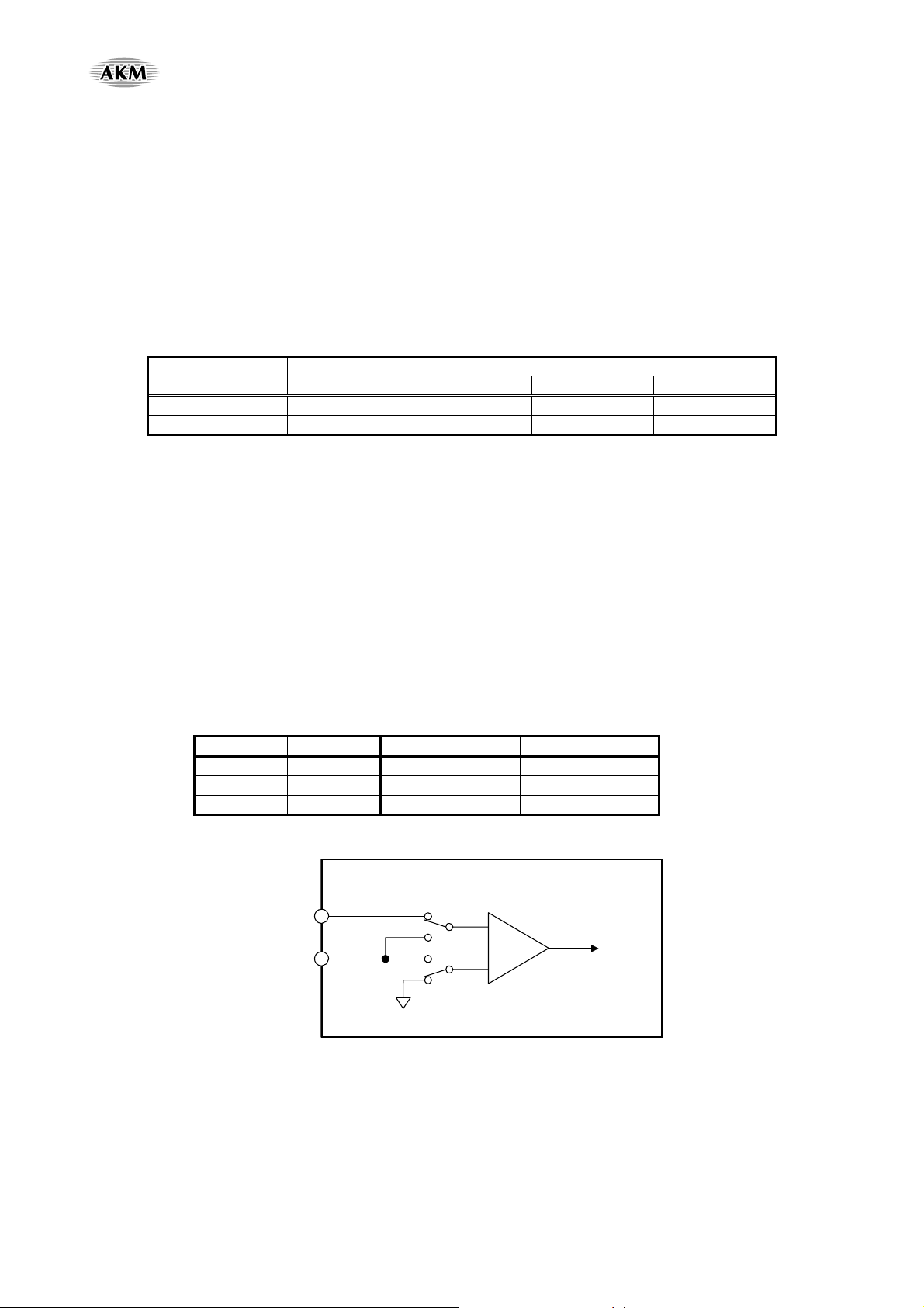
■ MIC/LINE Input Selector
The AK4646 has an input selector. When MDIF bit is “0”, LIN bit selects MIC pin or LIN pin. When MDIF bit is “1”,
full-differential input is available.
MDIF bit LIN bit Input circuit Input pin
0 0 Single-End MIC pin (default)
0 1 Single-End LIN pin
1 x Differential MICP/MICN pin
Table 19. Input Select (x: Don’t care)
MIC/MICP pin
LIN/MICN pin
AK4635
LIN bit
DC
MDIF bit
Figure 36 Input Selector
Rev. 0.6 2007/10
- 37 -

[AK4635]
HPF
AK4635
Audio
I/F
BICK pin
FCK pin
STDO pin
1k
1k
MPI pin
MICP pin
MICNpin
MIC-Power
A/D
MIC-Amp
Figure 37. MIC Differential Input Circuit
■ MIC Gain Amplifier
The AK4635 has a Gain Amplifier for Microphone input. These gains are selected by the MGAIN3-0 bit. The typical
input impedance is 30kΩ.
MGAIN3 bit MGAIN2 bit MGAIN1 bit MGAIN0 bit Input Gain
0 0 0 0 0dB
0 0 0 1 +20dB (default)
0 0 1 0 +26dB
0 0 1 1 +32dB
0 1 0 0 +10dB
0 1 0 1 +17dB
0 1 1 0 +23dB
0 1 1 1 +29dB
1 0 0 0 +3dB
1 0 0 1 +6dB
Others N/A
Table 20. Input Gain
■ MIC Power
The MPI pin supplies power for the Microphone. This output voltage is proportional to 0.8 x AVDD typically and the
load resistance is minimum 2kΩ. No capacitor must not be connected to the MPI pin, directly. (
MPI pin
MIC-Power
AK4635
Figure 38)
≥ 2k
MIC pin
MIC-Amp
A/D
HPF
Audio
I/F
BICK pin
FCK pin
STDO pin
Figure 38. MIC Block Circuit
Rev. 0.6 2007/10
- 38 -

[AK4635]
A
■ Digital Block
The digital block consists of block diagram as shown in Figure 39. The AK4635 can choose various signal processing on
a recording path or a playback path by setting ADCPF bit, PFDAC bit and PFSDO bit. (
PMADC bit
Figure 39 ~ Figure 42, Table 21)
HPFAD bit
1st Order
PMPFIL bit
“0” “1”
SDTO
ADC
HPF
HPF bit
LPF bit
EQ5-1 bits
PFSDO bit
SDTI
“1” “0”
DCPF bit
1st Order
HPF
1st Order
LPF
5 Band
EQ
ALC
(Volume)
“1” “0”
PFDAC bit
PMDAC bit
DATT
SMUTE
DAC
(1) ADC: Include the Digital Filter (LPF) for ADC as shown in “FILTER CHRACTERISTICS”.
(2) DAC: Include the Digital Filter (LPF) for DAC as shown in “FILTER CHRACTERISTICS”.
(3) HPF: High Pass Filter. Applicable to use as Wind-Noise Reduction Filter. (See “Programmable Filter”.)
(4) LPF: Low Pass Filter (See “Digital Programmable Filter”.)
(5) 5-Band EQ: Applicable to use as Equalizer or Notch Filter. (See “Digital Programmable Filter”.)
(6) ALC: Input Digital Volume with ALC function. (See “Input Digital Volume” and “ALC”.)
(7) DATT: 4-step Digital Volume for recording path. (See “Digital Volume 2”)
(8) SMUTE: Soft mute. (See “Soft Mute”.)
Figure 39. Digital Block Path Select
Rev. 0.6 2007/10
- 39 -

[AK4635]
Mode ADCPF bit PFDAC bit PFSDO bit Figure
Recording Mode 1 0 1 Figure 40
Reproduction Mode 0 1 0 Figure 41
Loop Back Mode 1 1 1 Figure 42
Table 21 Recording Reproduction Mode
ADC
2nd Order
HPF
1st Order
LPF
5 Band
EQ
ALC
(Volume)
DAC
DATTSMUTE
Figure 40. Path at Recording Mode (default)
ADC
DAC
1st Order
HPF
DATTSMUTE
ALC
(Volume)
5 Band
EQ
1st Order
LPF
1st Order
HPF
Figure 41. Path at Playback Mode
ADC
2nd Order
HPF
DAC
1st Order
LPF
DA TTSMUTE
5 Band
EQ
ALC
(Volume)
Figure 42. Path at Recording & Playback Mode
Rev. 0.6 2007/10
- 40 -

[AK4635]
A
■ Digital Programmable Filter Circuit
The AK4635 has 2 steps of 1st order HPF, 1st order LPF and 5-band Equalizer built-in in a recording path and a playback
path.
(1) High Pass Filter (HPF)
Normally, this HPF is used as a Wind-Noise Reduction Filter. This is composed with 2 steps of 1st order HPF. The
coefficient of both HPF is the same and set by F1A13-0 bits and F1B13-0 bits. HPFAD bit controls ON/OFF of the 1st
step HPF and HPF bit controls ON/OFF of the 2nd step HPF. When the HPF is OFF, the audio data passes this block by
0dB gain. The coefficient should be set when HPFAD = HPF bits = “0” or PMADC = PMPFIL bits = “0”.
fs : Sampling frequency
fc : Cut-off frequency
Register setting (
HPF: F1A[13:0] bits = A, F1B[13:0] bits = B
(MSB = F1A13, F1B13; LSB = F1A0, F1B0)
A =
The cut-off frequency should be set as below.
fc/fs ≥ 0.0001 (fc min = 1.6Hz at 16kHz)
(2) Low Pass Filter(LPF)
This is composed with 1st order LPF. F2A13-0 bits and F2B13-0 bits set the coefficient of LPF. LPF bit controls ON/OFF
of the LPF. When the LPF is OFF, the audio data passes this block by 0dB gain. The coefficient should be set when LPF
bit = “0” or PMPFIL bits = “0”.
fs : Sampling frequency
fc : Cut-off frequency
Register setting (
LPF: F2A[13:0] bits =A, F2B[13:0] bits =B
(MSB=F2A13, F1B13; LSB=F2A0, F2B0)
=
1 + 1 / tan (πfc/fs)
The cut-off frequency should be set as below.
fc/fs ≥ 0.05 (fc min = 2205Hz at 44.1kHz)
Note 38)
1
1 + tan (πfc/fs)
Note 38)
1
1− tan (πfc/fs)
B =
,
1 + tan (πfc/fs)
1 − 1 / tan (πfc/fs)
B =
,
1 + 1 / tan (πfc/fs)
Rev. 0.6 2007/10
- 41 -

[AK4635]
(3) 5-band Equalizer
This block can be used as Equalizer or Notch Filter. ON/OFF 5-band Equalizer (EQ1, EQ2, EQ3, EQ4 and EQ5) can be
controlled independently by EQ1, EQ2, EQ3, EQ4 and EQ5 bits. When Equalizer is OFF, the audio data passes this block
by 0dB gain. E1A15-0, E1B15-0 and E1C15-0 bits set the coefficient of EQ1. E2A15-0, E2B15-0 and E2C15-0 bits set
the coefficient of EQ2. E3A15-0, E3B15-0 and E3C15-0 bits set the coefficient of EQ3. E4A15-0, E4B15-0 and E4C15-0
bits set the coefficient of EQ4. E5A15-0, E5B15-0 and E5C15-0 bits set the coefficient of EQ5.
fs : The Sampling frequency
~ fo5 : The Center frequency
fo
1
~ fb5 : The Band width where the gain is 3dB different from center frequency
fb
1
~ K5 : The Gain ( -1 ≤ Kn < 3 )
K
1
Register setting (
EQ1: E1A[15:0] bits =A
EQ2: E2A[15:0] bits =A
EQ3: E3A[15:0] bits =A
EQ4: E4A[15:0] bits =A
EQ5: E5A[15:0] bits =A
Note 38)
, E1B[15:0] bits =B1, E1C[15:0] bits =C1
1
, E2B[15:0] bits =B2, E2C[15:0] bits =C2
2
, E3B[15:0] bits =B3, E3C[15:0] bits =C3
3
, E4B[15:0] bits =B4, E4C[15:0] bits =C4
4
, E5B[15:0] bits =B5, E5C[15:0] bits =C5
5
(MSB=E1A15, E1B15, E1C15, E2A15, E2B15, E2C15, E3A15, E3B15, E3C15, E4A15, E4B15, E4C15,
E5A15, E5B15, E5C15 ; LSB= E1A0, E1B0, E1C0, E2A0, E2B0, E2C0, E3A0, E3B0, E3C0, E4A0, E4B0,
E4C0, E5A0, E5B0, E5C0)
= Kn x
A
n
tan (πfb
/fs)
n
1 + tan (πfbn/fs)
, C
B
= cos(2π fon/fs) x
n
2
1 + tan (πfbn/fs)
1 − tan (πfb
=
n
,
/fs)
n
1 + tan (πfbn/fs)
(n = 1, 2, 3, 4, 5)
The center frequency should be set as below
/ fs < 0.497
fo
n
When gain of K is set to “−1”, the equalizer becomes notch filter. When it is used as notch filter, central frequency of a
real notch filter deviates from the above-mentioned calculation, if its central frequency of each band is near. The control
soft that is attached to the evaluation board has a function that revises a gap of frequency, and calculates the coefficient.
When its central frequency of each band is near, revise the central frequency and confirm the frequency response.
Note 38.
[Translation the filter coefficient calculated by the equations above from real number to binary code (2’s complement)]
X = (Real number of filter coefficient calculated by the equations above) x 2
13
X should be rounded to integer, and then should be translated to binary code (2’s complement).
MSB of each filter coefficient setting register is sine bit.
Rev. 0.6 2007/10
- 42 -

[AK4635]
■ Input Digital Volume (Manual Mode)
When ADCPF bit = “1” and ALC1 bit = “0”, ALC block becomes an input digital volume (manual mode). The digital
volume’s gain is set by IVOL7-0 bits as shown in
out. The zero crossing timeout period is set by ZTM1-0 bits.
IVOL7-0bits GAIN(0dB) Step
F1H +36.0
F0H +35.625
EFH +35.25
: :
92H +0.375
91H 0.0 (default)
90H -0.375
: :
2H -53.625
1H -54.0
0H MUTE
Table 22. Input Digital Volume Setting
When writing to the IVOL7-0 bits continually, the control register should be written in an interval more than zero
crossing timeout. If not, zero crossing counter could be reset at each time and volume is not be changed. However, it could
be ignored when writing the same register value as the last time. At this time, zero crossing counter has not been reset, so
it should be written in an interval less than zero crossing timeout.
Table 22. The IVOL value is changed at zero cross or zero cross time
0.375dB
Rev. 0.6 2007/10
- 43 -

[AK4635]
■ Output Digital volume (Manual mode)
When ADCPF bit = “0” and ALC2 bit = “0”, ALC block become an output digital volume (manual mode). The digital
volume’s gain is set by OVOL7-0 bits as shown in
at zero cross or zero cross time out. The zero crossing timeout period is set by ZTM1-0 bits.
OVOL7-0bits GAIN(0dB) Step
F1H +36.0
F0H +35.625
EFH +35.25
: :
92H +0.375
91H 0.0 (default)
90H -0.375
: :
2H -53.625
1H -54.0
0H MUTE
Table 23 Output Digital Volume Setting
When writing to the OVOL7-0 bits continually, the control register should be written by an interval more than zero
crossing timeout. If not, zero crossing counter could be reset at each time and volume is not be changed. However, It
could be ignored when writing a same register value as the last time. At this time, zero crossing counter has not been reset,
so it should be written by an interval less than zero crossing timeout.
Table 23. The OVOL7-0 bits value are reflected to this output volume
0.375dB
■ Output Digital Volume2
AK4635 has 4 steps output volume in addition to the volume setting by OVOL7-0 bits. This volume is set by DATT1-0
bits as shown in
Table 24.
DATT1-0bits GAIN(0dB) Step
0H 0.0 (default)
1H -6.0
2H -12.0
3H -18.1
Table 24. Output Digital Volume2 Setting
6.0dB
Rev. 0.6 2007/10
- 44 -

[AK4635]
■ ALC Operation
ALC Operation works in ALC block. When ADCPF bit = “1”, ALC operation is enable for recording path. When ADCPF
bit = “0”, ALC operation is enable for playback path. The ON/OFF of ALC operation for recording is controlled by ALC1
bit and the ON/OFF of ALC operation for playback is controlled by ALC2 bit.
1. ALC Limiter Operation
When the ALC limiter is enabled, and output exceeds the ALC limiter detection level (
attenuated by the amount defined in LMAT1-0 bits (
When the ZELMN bit = “0” (zero crossing detection valid), the VOL value is changed by ALC limiter operation at the
zero crossing point or zero crossing timeout. Zero crossing timeout period is set by ZTM1-0 bit that in common with ALC
recovery zero crossing timeout period’s setting (
(period : 1/fs) when output Level is over FS(Digital Full Scale).
When the ZELMN bit = “1” (zero crossing detection invalid), VOL value has been changed immediately (period: 1/fs) by
ALC limiter operation. The attenuation for limiter operation is fixed to 1 step and not controlled by setting LMAT1-0 bits.
After finishing the attenuation operation, if ALC bit does not change to “0”, the operation repeats when the output signal
level exceeds the ALC limiter detection level.
LMTH1 LMTH0 ALC Limiter Detection Level ALC Recovery Waiting Counter Reset Level
0 0
0 1
1 0
1 1
Table 25. ALC Limiter Detection Level / Recovery Waiting Counter Reset Level
LMAT1 LMAT0
0 0 1 1 1 1 (default)
0 1 2 2 2 2
1 0 2 4 4 8
1 1 1 2 4 8
ZTM1 ZTM0
0 0 128/fs 16ms 8ms 2.9ms (default)
0 1 256/fs 32ms 16ms 5.8ms
1 0 512/fs 64ms 32ms 11.6ms
1 1 1024/fs 128ms 64ms 23.2ms
ALC Output ≥ −2.5dBFS −2.5dBFS > ALC Output ≥ −4.1dBFS
ALC Output ≥ −4.1dBFS −4.1dBFS > ALC Output ≥ −6.0dBFS
ALC Output ≥ −6.0dBFS −6.0dBFS > ALC Output ≥ −8.5dBFS
ALC Output ≥ −8.5dBFS −8.5dBFS > ALC Output ≥ −12dBFS
ALC1 Output
≥ LMTH
Table 26. ALC Limiter ATT Step Setting
Zero Crossing Timeout Period
8kHz 16kHz 44.1kHz
Table 27. ALC Zero Crossing Timeout Period Setting
Table 26) automatically.
Table 27).At LFST bit = “1”, VOL value is attenuated 1step immediately
ALC1 Limiter ATT Step
ALC1 Output
≥ FS
ALC1 Output
≥ FS + 6dB
Table 25), the volume value is
(default)
ALC1 Output
≥ FS + 12dB
Rev. 0.6 2007/10
- 45 -

[AK4635]
2. ALC Recovery Operation
The ALC recovery operation waits for the WTM2-0 bits (
If the input signal does not exceed “ALC recovery waiting counter reset level” (
recovery operation is executed. The VOL value is automatically incremented by RGAIN1-0 bits (
reference level (
Table 30, Table 31) with zero crossing detection which timeout period is set by ZTM1-0 bits (Table 27).
Table 28) to be set after completing the ALC limiter operation.
Table 25) during the wait time, the ALC
Table 29) up to the set
The ALC recovery operation is executed in a period set by WTM2-0 bits.
For example, when the current VOL value is 30H and RGAIN1-0 bits are set to “01”(2 steps), VOL is changed to 32H by
the auto limiter operation and then the input signal level is gained by 0.75dB (=0.375dB x 2). When the VOL value
exceeds the reference level (IREF7-0 or OREF5-0), the VOL values are not increased.
When
“ALC recovery waiting counter reset level (LMTH1-0) ≤ Output Signal < ALC limiter detection level (LMTH1-0)”
during the ALC recovery operation, the waiting timer of ALC recovery operation is reset. When
“ALC recovery waiting counter reset level (LMTH1-0) > Output Signal”,
the waiting timer of ALC recovery operation starts.
The ALC operation corresponds to the impulse noise. When the impulse noise is input, the ALC recovery operation
becomes faster than a normal recovery operation. When large noise is input to microphone instantaneously, the quality of
small level in the large noise can be improved by this fast recovery operation. The speed of first recovery operation is set
by RFST1-0 bits (
Table 32).
WTM2 WTM1 WTM0
ALC Recovery Operation Waiting Period
8kHz 16kHz 44.1kHz
0 0 0 128/fs 16ms 8ms 2.9ms (default)
0 0 1 256/fs 32ms 16ms 5.8ms
0 1 0 512/fs 64ms 32ms 11.6ms
0 1 1 1024/fs 128ms 64ms 23.2ms
1 0 0 2048/fs 256ms 128ms 46.4ms
1 0 1 4096/fs 512ms 256ms 92.9ms
1 1 0 8192/fs 1024ms 512ms 185.8ms
1 1 1 16384/fs 2048ms 1024ms 371.5ms
Table 28. ALC Recovery Operation Waiting Period
RGAIN1 RGAIN0 GAIN STEP
0 0 1 0.375dB (default)
0 1 2 0.750dB
1 0 3 1.125dB
1 1 4 1.500dB
Table 29. ALC Recovery GAIN Step
Rev. 0.6 2007/10
- 46 -

[AK4635]
IREF7-0bits GAIN(0dB) Step
F1H +36.0
F0H +35.625
EFH +35.25
: :
C5H +19.5 (default)
: :
0.375dB
92H +0.375
91H 0.0
90H -0.375
: :
2H -53.625
1H -54.0
0H MUTE
Table 30. Reference Level at ALC Recovery operation for recoding
OREF5-0bits GAIN(0dB) Step
3CH +36.0
3BH +34.5
3AH +33.0
: :
28H +6.0 (default)
: :
1.5dB
25H +1.5
24H 0.0
23H -1.5
: :
2H -51.0
1H -52.5
0H -54.0
Table 31. Reference Level at ALC Recovery operation for playback
RFST1 bit RFST0 bit Recovery Speed
0 0 4 times (default)
0 1 8 times
1 0 16times
1 1 N/A
Table 32. First Recovery Speed Setting (N/A: Not available)
Rev. 0.6 2007/10
- 47 -

[AK4635]
3. The Volume at the ALC Operation
The current volume value at the ALC operation is reflected by VOL7-0 bits. It is enable to check the current volume value
by reading the register value of VOL7-0 bits.
This function is available only at the time of 3-wire mode. The volume value at the ALC operation can
not be read in I
2
C mode.
VOL7-0bits GAIN(0dB)
F1H +36.0
F0H +35.625
EFH +35.25
: :
C5H +19.5
: :
92H +0.375
91H 0.0
90H
−0.375
: :
2H
1H
−53.625
−54.0
0H MUTE
Table 33. Value of VOL7-0 bits
4. Example of the ALC Operation for Recording Operation
Table 34 shows the examples of the ALC setting for mic recording.
Register Name Comment
Data Operation Data Operation
LMTH1-0 Limiter detection Level 01
fs=8kHz fs=16kHz
−4.1dBFS
01
−4.1dBFS
ZELM Limiter zero crossing detection 0 Enable 0 Enable
ZTM1-0 Zero crossing timeout period 00 16ms 01 16ms
Recovery waiting period
WTM2-0
*WTM1-0 bits should be more than or
000 16ms 001 16ms
equal to ZTM1-0 bits
IREF7-0 Maximum gain at recovery operation C5H 19.5dB C5H 19.5dB
IVOL7-0 Gain of IVOL C5H 19.5dB C5H 19.5dB
LMAT1-0 Limiter ATT step 00 1step 00 1step
LFST Fast Limiter Operation 1 ON 1 ON
RGAIN1-0 Recovery GAIN step 00 1 step 00 1 step
ALC1 ALC enable 1 Enable 1 Enable
FRSL1-0 Speed of Fast Recovery 00 4 times 00 4times
Table 34. Example of the ALC Setting (Recording)
Rev. 0.6 2007/10
- 48 -

[AK4635]
5. Example of ALC for Playback Operation
Table 35 shows the example of the ALC setting for playback.
Register Name Comment
Data Operation Data Operation
LMTH1-0 Limiter detection Level 01
fs=8kHz fs=16kHz
−4.1dBFS
01
−4.1dBFS
ZELM Limiter zero crossing detection 0 Enable 0 Enable
ZTM1-0 Zero crossing timeout period 00 16ms 01 16ms
Recovery waiting period
WTM2-0
*WTM1-0 bits should be more than or
000 16ms 001 16ms
equal to ZTM1-0 bits
OREF5-0 Maximum gain at recovery operation 28 +6dB 28 +6dB
OVOL7-0 Gain of IVOL 91 0dB 91 0dB
LFST Fast Limiter Operation 1 ON 1 ON
LMAT1-0 Limiter ATT step 00 1step 00 1step
RGAIN1-0 Recovery GAIN step 00 1 step 00 1 step
ALC2 ALC enable 1 Enable 1 Enable
FRSL1-0 Speed of Fast Recovery 00 4 times 00 4 times
Table 35. Examples of the ALC Setting (Play back)
Rev. 0.6 2007/10
- 49 -

[AK4635]
(
The following registers must not be changed during the ALC operation. These bits should be changed, after the ALC
operation is finished by ALC1 bit = ALC2 bit = “0” or PMPFIL bit = “0”. After ALC1 bit and ALC2 bit set to “0” or
PMPFIL bit sets to “0”, when ALC is restarted, the waiting time of zero crossing timeout is not needed.
LMTH1-0, LMAT1-0, WTM2-0, ZTM1-0, RGAIN1-0, IREF7-0/OREF7-0, ZELM, RFST1-0, LFST
Manual Mode
WR (ZTM1-0, WTM2-0)
WR (IREF7-0/OREF5-0)
Example:
Limiter = Zero crossing Enable
Recovery Cycle = 16ms@8kHz
Limiter and Recovery Step = 1
LFST = 1
Maximum Gain = +19.5dB
Limiter Detection Level = −4.1dBFS
ALC1 bit = “1”
WR (IVOL7-0/OVOL7-0)
WR (RGAIN1, LMTH1,RFST1-0)
WR (LFST,LMAT1 - 0, RGAIN0, ZELM N, LMTH0)
WR
ALC1= “1”)
*2
ALC Operation
*1
(1) Addr=06H, Data=00H
(2) Addr=08H, Data=C5H
(3) Addr=09H, Data=C5H
(4) Addr=0BH, Data=28H
(5) Addr=07H, Data=A1H
Note : WR : Write
*1: The value of volume at starting should be the same or smaller than REF’s.
*2: When setting ALC1 bit or ALC2 bit to “0”, the operation is shifted to manual mode after passing the zero crossing
time set by ZTM1-0 bits.
Figure 43. Registers set-up sequence at the ALC operation
Rev. 0.6 2007/10
- 50 -

[AK4635]
A
A
■ SOFTMUTE
Soft mute operation is performed in the digital input domain. When the SMUTE bit changes to “1”, the input signal is
attenuated by −∞ (“0”) during the cycle of 245/fs (31msec@fs=8kHz). When the SMUTE bit is returned to “0”, the mute
is cancelled and the input attenuation gradually changes to 0dB during the cycle of 245/fs (31msec@fs=8kHz). If the soft
mute is cancelled within the cycle of 245/fs (31msec@fs=8kHz), the attenuation is discontinued and returned to 0dB. The
soft mute for Playback operation is effective for changing the signal source without stopping the signal transmission.
SMUTE bit
tten u a tio n
nalog Output
0dB
-∞
245/fs
(1)
GD
(2)
245/fs
(3)
GD
Figure 44. Soft Mute Function
(1) The input signal is attenuated by −∞ (“0”) during the cycle of 245/fs (31msec@fs=8kHz).
(2) Analog output corresponding to digital input has the group delay (GD).
(3) If the soft mute is cancelled within the cycle of 245/fs (31msec@fs=8kHz), the attenuation is discounted and returned
to 0dB within the same cycle.
Rev. 0.6 2007/10
- 51 -

[AK4635]
Ω
Ω
A
A
■ MONO LINE OUTPUT (AOUT pin)
A signal of DAC is output from the AOUT pin. When the DACA bit is “0”, this output is OFF. When the LOVL bit is “1”,
this gain changes to +2dB. The load resistance is 10kΩ(min). When PMAO bit is “0” and AOPSN bit is “0”, the mono
line output enters power-down and is pulled down by 100Ω(typ). If PMAO bit is controlled at AOPS bit = “1”, POP noise
will be reduced at power-up and down. Then, this line should be pulled down by 20kΩ of resister after C-coupling shown
in
Figure 45. This rising and falling time is max 300 ms at C = 1.0μF . When PMAO bit is “1” and AOPS bit is “0”, the
mono line output enters power-up state.
LOVL bits Gain
0 0dB (default)
1 +2dB
Table 36. Mono line output volume setting
AOUT
1μF
220
20k
Figure 45. AOUT external circuit when using POP Reduction function
AOUT Control Sequence in case of using POP Reduction Circuit
P M A O bit
OPS bit
OU T pin
(1)
(2)
(3) (4)
Normal Output
≥ 300 ms ≥ 300 ms
(5)
Figure 46. Mono Line Output Control Sequence when using POP Reduction function
(1) Set AOPS bit = “1”. Mono line output enters the power-save mode.
(2) Set PMAO bit = “1”. Mono line output exits the power-down mode.
AOUT pin rises up to VCOM voltage. Rise time is 200ms (max 300ms) at C=1μF.
(3) Set AOPS bit = “0” after AOUT pin rises up. Mono line output exits the power-save mode.
Mono line output is enabled.
(4) Set AOPS bit = “1”. Mono line output enters power-save mode.
(5) Set PMAO bit = “1”. Mono line output enters power-down mode.
AOUT pin falls down to VSS1. Fall time is 200ms (max 300ms) at C=1μF.
(6) Set AOPS bit = “0” after AOUT pin falls down. Mono line output exits the power-save mode.
(6)
Rev. 0.6 2007/10
- 52 -

[AK4635]
■ Speaker Output
AK4635 has a Mono Class-D Speaker-Amp. Power supply for Speaker-Amp(SVDD) can be set from 2.2V up to 4.0V.
The Speaker is mono and BTL output, and can drive dynamic speaker and piezo speaker without LPF (filter-less). This
speaker can output 400W@8Ω at SVDD = 3.3V, SPKG bit = “0”. This gain is set by SPKG bit (
level of speaker amp is depended on voltage of SVDD and SPKG bit.
SPKG bit Gain
0 0dB
1 +2dB (Note 39)
Note 39. The signals more than -2dBFS clip.
Table 37. SPK- Amp Gain
The power up/down speaker amp is controlled by PMSPK bit. When PMSPK bit is “0”, the SPP and SPN pins output
VSS3 level. Also ON/OFF of speaker amp is controlled by SPOUTE bit. When SPOUTE bit is “0”, the SPP and SPN pins
are in VSS3-state forcibly. When the outputting from DAC to speaker, PMDAC bit should be set to “1”.
Follow the following sequence.
PMSP K bit
Table 37). The output
S P O U T E b it
SPP pin
SPN pin
N o rm al O u tp u t
Normal Output
Figure 47. Power-up/Power-down Timing for Speaker-Amp
Rev. 0.6 2007/10
- 53 -

[AK4635]
Ω
Ω
<Caution for using Piezo Speaker>
When a piezo speaker is used, resistances more than 10Ω should be connected between the SPP/SPN pins and speaker in
series, respectively, as shown in
Figure 48. Zener diodes should be connected between speaker and GND as shown in
Figure 48, in order to protect SPK-Amp of the AK4635 from the power that is the piezo speaker output when the speaker
is pressured. Zener diodes of the following Zener voltage should be used.
92% of SVDD ≤ Zener voltage of Zener diodo(ZD of
Figure 48) ≤ SVDD+0.3V
Ex) In case of SVDD = 3.8V :3.5V ≤ ZD ≤ 4.1V
For example, Zener diode which Zener voltage is 3.9V(Min 3.7V, Max 4.1V) can be used.
ZD
SPK-Amp
SPP
SPN
≥10
≥10
ZD
Figure 48. Circuit of Speaker Output (using a piezo speaker)
Rev. 0.6 2007/10
- 54 -

[AK4635]
p
p
■ BEEP Generate
The AK4635 generates and output square wave from speaker amp. After outputting the signal during the time set by
BPON6-0 bits, the AK4635 stops the output signal during the time set by BPOFF6-0 bits (
set by BPTM6-0 bit, and the output level is set by BPLVL2-0 bits. When BPCNT bit is “0”, if BPOUT bit is written “1”,
the AK4635 outputs the beep for the times of repeat count. When the output finish, BPOUT bit is set to “0” automatically.
When BPCNT bit is set to “1”, it outputs the beep in succession regardless of repeat count, on-time and off-time.
< Setting parameter >
1) Output Frequency (
2) ON Time (
3) OFF Time (
Table 41)
Table 42)
4) Repeat Count (
5) Output Level (
Table 38 ~ Table 40)
Table 43)
Table 44)
BPFR1-0, BPON7-0, BPOFF7-0, BPTM6-0 and BPLVL3-0 bits should be set when BPOUT =BPCNT
= “0”.
BPCNT bit is given priority in BPOUT bit. When BPOUT bit be set to “1”, if BPCNT bit is set to “0”,
BPOUT bit is set to “0” forcibly.
Figure 50). The repeat count is
BEEP
Generator
DATT2
SMUTE
LPF
DAC
Line Out Am
Class-D SPK-Am
Figure 49. BEEP signal output path
BEEP Output
ON Time OFF Time
Repeat Count
Figure 50. Beep output
Rev. 0.6 2007/10
- 55 -

[AK4635]
Output frequency of BEEP Generator [Hz]
BPFR1-0 bit fs = 48kHz system
Note 40)
(
fs = 44.1kHz system
(Note 41)
00 4000 4009 (default)
01 2000 2005
10 1000 1002
11 N/A
Note 40. Sampling frequency is 8kHz, 16kHz, 32kHz or 48kHz.
Note 41. Sampling frequency is 11.025kHz, 22.05kHz or 44.1kHz.
Table 38. Beep signal frequency (PLL Master/Slave Mode: reference clock: MCKI) (N/A: Not available)
Output frequency of BEEP Generator [Hz]
BPFR1-0 bit FS3-2 bits = “00” FS3-2 bits = “01” FS3-2 bits = “10”
00 fs/2.75 fs/5.5 fs/11 (default)
01 fs/5.5 fs/11 fs/22
10 fs/11 fs/22 fs/44
11 N/A
Table 39. Beep signal frequency ( PLL Slave Mode: reference clock : FCK/BICK) (N/A: Not available)
Output frequency of BEEP Generator [Hz]
BPFR1-0 bit FS1-0 bits = “00” FS1-0 bits = “01” FS1-0 bits = “10” FS1-0 bits = “11”
00 fs/11 fs/2.75 fs/55 fs/11 (default)
01 fs/22 fs/5.5 fs/11 fs/22
10 fs/44 fs/11 fs/22 fs/44
11 N/A
Table 40. Beep signal frequency (EXT Slave/Master Mode) (N/A: Not available)
ON Time of BEEP Generator [msec] Step [msec]
BPON7-0 bit fs = 48kHz
system
Note 40)
(
fs = 44.1kHz
system
Note 41)
(
fs = 48kHz
system
Note 40)
(
fs = 44.1kHz
system
Note 41)
(
0H 8.0 7.98 8.0 7.98 (default)
1H 16.0 15.86
2H 24.0 23.95
3H 32.0 31.93
4H 40.0 39.9
: :
FDH 2032 2027.3
FEH 2040 2035.3
FFH 2048 2043.4
Note 40. Sampling frequency is 8kHz, 16kHz, 32kHz or 48kHz.
Note 41. Sampling frequency is 11.025kHz, 22.05kHz or 44.1kHz.
Table 41. Beep output ON-time (PLL Master/Slave Mode reference clock: MCKI)
Rev. 0.6 2007/10
- 56 -

[AK4635]
OFF Time of BEEP Generator [msec] Step [msec]
BPOFF7-0 bit fs = 48kHz
system
Note 40)
(
fs = 44.1kHz
system
Note 41)
(
fs = 48kHz
system
Note 40)
(
fs = 44.1kHz
system
Note 41)
(
0H 8.0 7.98 8.0 7.98 (default)
1H 16.0 15.86
2H 24.0 23.95
3H 32.0 31.93
4H 40.0 39.9
: :
FDH 2032 2027.3
FEH 2040 2035.3
FFH 2048 2043.4
Note 40. Sampling frequency is 8kHz, 16kHz, 32kHz or 48kHz.
Note 41. Sampling frequency is 11.025kHz, 22.05kHz or 44.1kHz.
Table 42. Beep output OFF-time (PLL Master/Slave Mode reference clock: MCKI)
BPTM6-0 bit Repeat Count
0H 1 (default)
1H 2
2H 3
3H :
: 125
7DH 126
7EH 127
7FH 128
Table 43. Beep output Repeat Count
BPLVL3-0 bit .Beep Output Level STEP
0H 0dB (default)
1H
2H
3H
4H
5H
6H
7H
−3dB
−6dB
−9dB
−12dB
−18dB
−24dB
−30dB
3dB
6dB
Note 42. Power supply is 3.3V
Note 43. Beep output amplitude as 0dB setting is 4.4Vpp@ load resistance = 8Ω + 10µH, SVDD=3.3V
Table 44. Beep output level
Rev. 0.6 2007/10
- 57 -

[AK4635]
■ Video Block
Video-Amp has a drivability for a load resistance of 150Ω. The AK4635 has a composite input and output. A Low Pass
Filter (LPF) and Gain Control Amp (GCA) are integrated and both DC output and Sag Compensation circuit are
supported as shown in
47µF+4.7µF. When DC output is used, the VOUT pin and the VSAG pin must be shorted. The output clamp voltage is 50
mV(typ) at DC output. SAGC bit should be set as shown in
SAGC bit = “1”. The gain can be set by VGCA4-0 bits. PMV bit controls the power up and down of the video block. The
VOUT pin outputs VSS1 level at PMV bit = “0”.
Figure 51 and Figure 52. The capacitance for Sag Compensation circuit is 100µF+4.7µF or
Table 45.VSAG2-0 bits should be set as shown in Table 46 at
C1
VIN
CLAMP
LPF GCA
-1dB ~ +10.5dB
Step 0.5dB
+6dB
VOUT
VSAG
75Ω
C2
(C1=100μ F, C2=4.7μ F) or (C1=47μ F, C2=4.7μ F)
Figure 51 Video block (using Sag Compensation circuit)
VIN
CLAMP
LPF GCA
-1dB ~ +10.5dB
Step 0.5dB
+6dB
VOUT
VSAG
75Ω
Figure 52. Video block (at DC Output)
Rev. 0.6 2007/10
- 58 -

[AK4635]
SAGC bit Output Method
0 DC Output (default)
1 Sag Compensation circuit
Table 45. Output method setting
VSAG2 bit VSAG1 bit VSAG0 bit External capacitance
0 1 1 C1 = 100μF,C2 = 4.7μF
1 0 1 C1 = 47μF,C2 = 4.7μF (default)
Others N/A
Table 46. Sag Compensation circuit setting (SACG bit = “1”) (N/A: Not available)
VGCA4-0 bits GAIN(dB) STEP
17H +10.5dB
16H +10.0dB
15H +9.5dB
: :
04H +1.0dB
03H +0.5dB
02H 0.0dB (default)
01H −0.5dB
00H −1.0dB
Table 47. Video signal gain setting
0.5dB
Rev. 0.6 2007/10
- 59 -

[AK4635]
■ Serial Control Interface
(1) 3-wire Serial Control Mode (I2C pin = “L”)
Internal registers may be written and read by using the 3-wire µP interface pins (CSN, CCLK and CDTIO). The data on
this interface consists of Read/Write, Register address (MSB first, 7bits) and Control data (MSB first, 8bits). Address and
data is clocked in on the rising edge of CCLK and data is clocked out on the falling edge. Data writing is valid on the
rising edge of the 16th CCLK after the falling edge of CSN. CSN should be set to “H” every after a data writing for each
address. In reading operation, the CDTIO pin changes to output mode at the falling edge of 8th CCLK and outputs
D7-D0. The output finishes on the rising edge of CSN. However this reading function is available only at READ bit = “1”.
When READ bit = “0”, the CDTIO pin stays as Hi-Z even after the falling edge of 8th CCLK. The CDTIO pin is placed
in a Hi-Z state except outputting data at read operation mode. The clock speed of CCLK is 5MHz (max). The value of
internal registers is initialized at the PDN pin = “L”.
Note 44. It is available for reading the address 00H ~ 11H, 20H ~ 24H and 30H. When reading the address 12H ~ 1FH,
25H ~ 2F and 31H ~ 4FH, the register values are invalid.
CSN
6 7 8 9 10 11
12 13 14 15
Clock, “H” or “L” Clock, “H” or “L”
CCLK
CDTIO
0 1 2 3 4 5
“H” or “L” “H” or “L”
A6 A5 A2 A3 A1 A0 A4 D7 D6 D5 D4 D3 D2 D1 D0
R/W
R/W: READ/WRITE (“1”: WRITE, “0”: READ)
A6-A0: Register Address
D7-D0: Control data
Figure 53. Serial Control I/F Timing
Rev. 0.6 2007/10
- 60 -

[AK4635]
(2) I2C-bus Control Mode (I2C pin = “H”)
The AK4635 supports the fast-mode I
2
C-bus (max: 400kHz). Pull-up resistors at SDA and SCL pins should be connected
to (DVDD+0.3)V or less voltage.
(2)-1. WRITE Operations
Figure 54 shows the data transfer sequence for the I2C-bus mode. All commands are preceded by a START condition. A
HIGH to LOW transition on the SDA line while SCL is HIGH indicates a START condition (
Figure 60). After the
START condition, a slave address is sent. This address is 7 bits long followed by the eighth bit that is a data direction bit
(R/W). The most significant seven bits of the slave address are fixed as “0010010” (
Figure 55). If the slave address
matches that of the AK4635, the AK4635 generates an acknowledge and the operation is executed. The master must
generate the acknowledge-related clock pulse and release the SDA line (HIGH) during the acknowledge clock pulse
Figure 61). A R/W bit value of “1” indicates that the read operation is to be executed. A “0” indicates that the write
(
operation is to be executed.
The second byte consists of the control register address of the AK4635. The format is MSB first, and those most
significant 1-bits are fixed to zeros (
first, 8bits (
Figure 57). The AK4635 generates an acknowledge after each byte is received. A data transfer is always
Figure 56). The data after the second byte contains control data. The format is MSB
terminated by a STOP condition generated by the master. A LOW to HIGH transition on the SDA line while SCL is
HIGH defines a STOP condition (
Figure 60).
The AK4635 can perform more than one byte write operation per sequence. After receipt of the third byte the AK4635
generates an acknowledge and awaits the next data. The master can transmit more than one byte instead of terminating the
write cycle after the first data byte is transferred. After receiving each data packet the internal 6-bit address counter is
incremented by one, and the next data is automatically taken into the next address. If the address exceeds 4FH prior to
generating a stop condition, the address counter will “roll over” to 00H and the previous data will be overwritten.
The data on the SDA line must remain stable during the HIGH period of the clock. The HIGH or LOW state of the data
line can only change when the clock signal on the SCL line is LOW (
Figure 62) except for the START and STOP
conditions.
SDA
S
T
A
R
T
S
Slave
Address
R/W="0"
Sub
Address(n)
A
C
K
Data(n)
A
C
K
Figure 54. Data Transfer Sequence at the I
A
C
K
Data(n+1)
2
A
C
K
C-Bus Mode
Data(n+x)
A
C
K
S
T
O
P
P
A
C
K
0 0 1 0 0 1 0 R/W
Figure 55. The First Byte
0 A6 A5 A4 A3 A2 A1 A0
Figure 56. The Second Byte
D7 D6 D5 D4 D3 D2 D1 D0
Figure 57. Byte Structure after the second byte
Rev. 0.6 2007/10
- 61 -

[AK4635]
(2)-2. READ Operations
Set the R/W bit = “1” for READ operation of the AK4635. After transmission of data, the master can read the next
address’s data by generating an acknowledge instead of terminating the write cycle after the receipt of the first data word.
After receiving each data packet the internal 6-bit address counter is incremented by one, and the next data is
automatically taken into the next address. If the address exceeds 4FH prior to generating a stop condition, the address
counter will “roll over” to 00H and the data of 00H will be read out.
Note 44. It is available for reading the address 00H ~ 11H, 20H ~ 24H and 30H. When reading the address 12H ~ 1FH,
25H ~ 2F and 31H ~ 4FH, the register values are invalid.
The AK4635 supports two basic read operations: CURRENT ADDRESS READ and RANDOM ADDRESS READ.
(2)-2-1. CURRENT ADDRESS READ
The AK4635 contains an internal address counter that maintains the address of the last word accessed, incremented by
one. Therefore, if the last access (either a read or write) were to address n, the next CURRENT READ operation would
access data from the address n+1. After receipt of the slave address with R/W bit “1”, the AK4635 generates an
acknowledge, transmits 1-byte of data to the address set by the internal address counter and increments the internal
address counter by 1. If the master does not generate an acknowledge but instead generates a stop condition, the AK4635
ceases transmission.
SDA
S
T
A
R
T
S
Slave
Address
R/W="1"
Data(n)
A
C
K
M
A
S
T
E
R
A
C
K
Data(n+1)
M
A
S
T
E
R
A
C
K
Data(n+2)
Data(n+x)
M
M
A
S
T
E
R
A
A
A
C
C
S
K
K
T
E
R
S
T
O
P
P
M
N
A
A
S
C
T
K
E
R
Figure 58. CURRENT ADDRESS READ
(2)-2-2. RANDOM ADDRESS READ
The random read operation allows the master to access any memory location at random. Prior to issuing the slave address
with the R/W bit “1”, the master must first perform a “dummy” write operation. The master issues a start request, a slave
address (R/W bit = “0”) and then the register address to read. After the register address is acknowledged, the master
immediately reissues the start request and the slave address with the R/W bit set to “1”. The AK4635 then generates an
acknowledge, 1 byte of data and increments the internal address counter by 1. If the master does not generate an
acknowledge but instead generates a stop condition, the AK4635 ceases transmission.
S
T
A
R/W="1"
R
T
Slave
S
Address
A
C
K
Data(n)
A
C
K
Data(n+1)
M
A
A
C
S
K
T
E
R
M
A
A
C
S
K
T
E
R
Data(n+x)
M
A
A
C
S
K
T
E
R
S
T
O
P
P
M
N
A
A
S
C
T
K
E
R
SDA
S
T
A
R
T
S
Slave
Address
R/W="0"
A
C
K
Sub
Address(n)
Figure 59. RANDOM ADDRESS READ
Rev. 0.6 2007/10
- 62 -

[AK4635]
SDA
SCL
DATA
OUTPUT BY
TRANSMITTER
DATA
OUTPUT BY
RECEIVER
SCL FROM
MASTER
S
START
CONDITION
S
Figure 60. START and STOP Conditions
1 98
Figure 61. Acknowledge on the I
2
2
C-Bus
P
stop conditionstart condition
not acknowledge
acknowledge
clock pulse for
acknowledgement
SDA
SCL
data line
stable;
data valid
Figure 62. Bit Transfer on the I
change
of data
allowed
2
C-Bus
Rev. 0.6 2007/10
- 63 -

[AK4635]
■ Register Map
Addr Register Name D7 D6 D5 D4 D3 D2 D1 D0
00H Power Management 1 PMPFIL PMVCM 0 PMSPK PMAO PMDAC 0 PMADC
01H Power Management 2 PMV 0 0 0 M/S 0 MCKO PMPLL
02H Signal Select 1 SPOUTE 0 DACS DACA MGAIN3 PMMP MGAIN2 MGAIN0
03H Signal Select 2 PFSDO AOPS MGAIN1 0 SPKG 0 PFDAC ADCPF
04H Mode Control 1 PLL3 PLL2 PLL1 PLL0 BCKO1 BCKO0 DIF1 DIF0
05H Mode Control 2 ADRST FCKO FS3 MSBS BCKP FS2 FS1 FS0
06H Timer Select 0 WTM2 ZTM1 ZTM0 WTM1 WTM0 RFST1 RFST0
07H ALC Mode Control 1 LFST ALC2 ALC1 ZELMN LMAT1 LMAT0 RGAIN0 LMTH0
08H ALC Mode Control 2 IREF7 IREF6 IREF5 IREF4 IREF3 IREF2 IREF1 IREF0
09H Digital Volume Control IVOL7 IVOL6 IVOL5 IVOL4 IVOL3 IVOL2 IVOL1 IVOL0
0AH Digital Volume Control OVOL7 OVOL6 OVOL5 OVOL4 OVOL3 OVOL2 OVOL1 OVOL0
0BH ALC Mode Control 3 RGAIN1 LMTH1 OREF5 OREF4 OREF3 OREF2 OREF1 OREF0
0CH Video Mode Control 0 0 SAGC VGCA4 VGCA3 VGCA2 VGCA1 VGCA0
0DH ALC LEVEL VOL7 VOL6 VOL5 VOL4 VOL3 VOL2 VOL1 VOL0
0EH Signal Select 3 DATT1 DATT0 SMUTE MDIF VSAG2 VSAG1 VSAG0 READ
0FH Thermal Shutdown THDET 0 0 0 0 0 0 0
10H Signal Select 4 0 LOVL 0 0 0 0 LIN 0
11H Digital Filter Select 1 0 0 LPF HPF 0 0 0 HPFAD
12H Reserved 0 0 0 0 0 0 0 0
13H Reserved 0 0 0 0 0 0 0 0
14H Reserved 0 0 0 0 0 0 0 0
15H Reserved 0 0 0 0 0 0 0 0
16H Reserved 0 0 0 0 0 0 0 0
17H Reserved 0 0 0 0 0 0 0 0
18H Reserved 0 0 0 0 0 0 0 0
19H Reserved 0 0 0 0 0 0 0 0
1AH Reserved 0 0 0 0 0 0 0 0
1BH Reserved 0 0 0 0 0 0 0 0
1CH HPF Co-efficient 0 F1A7 F1A6 F1A5 F1A4 F1A3 F1A2 F1A1 F1A0
1DH HPF Co-efficient 1 0 0 F1A13 F1A12 F1A11 F1A10 F1A9 F1A8
1EH HPF Co-efficient 2 F1B7 F1B6 F1B5 F1B4 F1B3 F1B2 F1B1 F1B0
1FH HPF Co-efficient 3 0 0 F1B13 F1B12 F1B11 F1B10 F1B9 F1B8
20H BEEP Frequency BPCNT 0 0 0 0 0 BPFR1 BPFR0
21H BEEP ON Time BPON7 BPON6 BPON5 BPON4 BPON3 BPON2 BPON1 BPON0
22H BEEP OFF Time BPOFF7 BPOFF6 BPOFF5 BPOFF4 BPOFF3 BPOFF2 BPOFF1 BPOFF0
23H BEEP Repeat Count 0 BPTM6 BPTM5 BPTM4 BPTM3 BPTM2 BPTM1 BPTM0
24H BEEP VOL/Control BPOUT 0 0 0 0 BPLVL2 BPLVL1 BPLVL0
25H Reserved 0 0 0 0 0 0 0 0
26H Reserved 0 0 0 0 0 0 0 0
27H Reserved 0 0 0 0 0 0 0 0
28H Reserved 0 0 0 0 0 0 0 0
29H Reserved 0 0 0 0 0 0 0 0
2AH Reserved 0 0 0 0 0 0 0 0
2BH Reserved 0 0 0 0 0 0 0 0
2CH LPF Co-efficient 0 F2A7 F2A6 F2A5 F2A4 F2A3 F2A2 F2A1 F2A0
2DH LPF Co-efficient 1 0 0 F2A13 F2A12 F2A11 F2A10 F2A9 F2A8
2EH LPF Co-efficient 2 F2B7 F2B6 F2B5 F2B4 F2B3 F2B2 F2B1 F2B0
2FH LPF Co-efficient 3 0 0 F2B13 F2B12 F2B11 F2B10 F2B9 F2B8
Rev. 0.6 2007/10
- 64 -

[AK4635]
Addr Register Name D7 D6 D5 D4 D3 D2 D1 D0
30H Digital Filter Select 2 0 0 0 EQ5 EQ4 EQ3 EQ2 EQ1
31H Reserved 0 0 0 0 0 0 0 0
32H E1 Co-efficient 0 E1A7 E1A6 E1A5 E1A4 E1A3 E1A2 E1A1 E1A0
33H E1 Co-efficient 1 E1A15 E1A14 E1A13 E1A12 E1A11 E1A10 E1A9 E1A8
34H E1 Co-efficient 2 E1B7 E1B6 E1B5 E1B4 E1B3 E1B2 E1B1 E1B0
35H E1 Co-efficient 3 E1B15 E1B14 E1B13 E1B12 E1B11 E1B10 E1B9 E1B8
36H E1 Co-efficient 4 E1C7 E1C6 E1C5 E1C4 E1C3 E1C2 E1C1 E1C0
37H E1 Co-efficient 5 E1C15 E1C14 E1C13 E1C12 E1C11 E1C10 E1C9 E1C8
38H E2 Co-efficient 0 E2A7 E2A6 E2A5 E2A4 E2A3 E2A2 E2A1 E2A0
39H E2 Co-efficient 1 E2A15 E2A14 E2A13 E2A12 E2A11 E2A10 E2A9 E2A8
3AH E2 Co-efficient 2 E2B7 E2B6 E2B5 E2B4 E2B3 E2B2 E2B1 E2B0
3BH E2 Co-efficient 3 E2B15 E2B14 E2B13 E2B12 E2B11 E2B10 E2B9 E2B8
3CH E2 Co-efficient 4 E2C7 E2C6 E2C5 E2C4 E2C3 E2C2 E2C1 E2C0
3DH E2 Co-efficient 5 E2C15 E2C14 E2C13 E2C12 E2C11 E2C10 E2C9 E2C8
3EH E3 Co-efficient 0 E3A7 E3A6 E3A5 E3A4 E3A3 E3A2 E3A1 E3A0
3FH E3 Co-efficient 1 E3A15 E3A14 E3A13 E3A12 E3A11 E3A10 E3A9 E3A8
40H E3 Co-efficient 2 E3B7 E3B6 E3B5 E3B4 E3B3 E3B2 E3B1 E3B0
41H E3 Co-efficient 3 E3B15 E3B14 E3B13 E3B12 E3B11 E3B10 E3B9 E3B8
42H E3 Co-efficient 4 E3C7 E3C6 E3C5 E3C4 E3C3 E3C2 E3C1 E3C0
43H E3 Co-efficient 5 E3C15 E3C14 E3C13 E3C12 E3C11 E3C10 E3C9 E3C8
44H E4 Co-efficient 0 E4A7 E4A6 E4A5 E4A4 E4A3 E4A2 E4A1 E4A0
45H E4 Co-efficient 1 E4A15 E4A14 E4A13 E4A12 E4A11 E4A10 E4A9 E4A8
46H E4 Co-efficient 2 E4B7 E4B6 E4B5 E4B4 E4B3 E4B2 E4B1 E4B0
47H E4 Co-efficient 3 E4B15 E4B14 E4B13 E4B12 E4B11 E4B10 E4B9 E4B8
48H E4 Co-efficient 4 E4C7 E4C6 E4C5 E4C4 E4C3 E4C2 E4C1 E4C0
49H E4 Co-efficient 5 E4C15 E4C14 E4C13 E4C12 E4C11 E4C10 E4C9 E4C8
4AH E5 Co-efficient 0 E5A7 E5A6 E5A5 E5A4 E5A3 E5A2 E5A1 E5A0
4BH E5 Co-efficient 1 E5A15 E5A14 E5A13 E5A12 E5A11 E5A10 E5A9 E5A8
4CH E5 Co-efficient 2 E5B7 E5B6 E5B5 E5B4 E5B3 E5B2 E5B1 E5B0
4DH E5 Co-efficient 3 E5B15 E5B14 E5B13 E5B12 E5B11 E5B10 E5B9 E5B8
4EH E5 Co-efficient 4 E5C7 E5C6 E5C5 E5C4 E5C3 E5C2 E5C1 E5C0
4FH E5 Co-efficient 5 E5C15 E5C14 E5C13 E5C12 E5C11 E5C10 E5C9 E5C8
The PDN pin = “L” resets the registers to their default values.
Note 45. Unused bits must contain a “0” value.
Note 46. Reading of address 12H ~ 1FH, 25H ~ 2FH and 31H ~ 4FH are not possible.
Note 47. 0FH and 0DH are for address read only. However, 0DH address cannot be read at I
2
C –bus control mode.
Writing access to 0DH and 0FH does not effect the operation.
Rev. 0.6 2007/10
- 65 -

[AK4635]
■ Register Definitions
Addr Register Name D7 D6 D5 D4 D3 D2 D1 D0
00H Power Management 1 PMPFIL PMVCM 0 PMSPK PMAO PMDAC 0 PMADC
R/W R/W R/W R R/W R/W R/W R R/W
Default 0 0 0 0 0 0 0 0
PMADC: ADC Block Power Control
0: Power down (default)
1: Power up
When the PMADC bit changes from “0” to “1”, the initialization cycle (1059/fs=133ms@8kHz) starts. After
initializing, digital data of the ADC is output.
PMDAC: DAC Block Power Control
0: Power down (default)
1: Power up
PMAO: Mono Line Out Power Control
0: Power down (default)
1: Power up
PMSPK: Speaker Block Power Control
0: Power down (default)
1: Power up
PMVCM: VCOM Block Power Control
0: Power down (default)
1: Power up
PMPFIL: Programmable Filter Block (HPF/ LPF/ 5-Band EQ/ ALC) Power Control
0: Power down (default)
1: Power up
Each block can be powered-down respectively by writing “0” to each bit. When the PDN pin is “L”, all blocks are
powered-down.
When PMPLL and MCKO bits and all bits in 00H address are “0”, all blocks are powered-down.
When any of the blocks are powered-up, the PMVCM bit must be set to “1”. When PMPLL and MCKO bits and all
bits in 00H address are “0”, PMVCM bit can be “0”.
When any block of ADC, DAC, SPK, or Programmable digital filter is powered-up (PMADC bit = “1”or PMDAC bit
= “1” or PMSPK bit = “1” PMPFIL bit = “1”), the clocks must always be present.
Rev. 0.6 2007/10
- 66 -

[AK4635]
Addr Register Name D7 D6 D5 D4 D3 D2 D1 D0
01H Power Management 2 PMV 0 0 0 M/S 0 MCKO PMPLL
R/W R/W R R R R/W R R/W R/W
Default 0 0 0 0 0 0 0 0
PMPLL: PLL Block Power Control Select
0: PLL is Power down and External is selected. (default)
1: PLL is Power up and PLL Mode is selected.
MCKO: Master Clock Output Enable
0: “L” Output (default)
1: 256fs Output
M/S: Select Master/ Slave Mode
0: Slave Mode (default)
1: Master Mode
PMV: Video Block Power Control
0: Power down (default)
1: Power up
Addr Register Name D7 D6 D5 D4 D3 D2 D1 D0
02H Signal Select 1 SPOUTE 0 DACS DACA MGAIN3 PMMP MGAIN2 MGAIN0
R/W R/W R R/W R/W R/W R/W R/W R/W
Default 0 0 0 0 0 0 0 1
MGAIN3-2: MIC-amp Gain control (
Table 20)
MGAIN1 bit is located at D5 bit of 03H. Default: “0001” (+20.0dB)
PMMP: MPI pin Power Control
0: Power down (default)
1: Power up
When PMADC bit is “1”, PMMP bit is enabled.
DACA: Switch Control from DAC to mono line amp
0: OFF (default)
1: ON
When PMAO bit is “1”, DACA bit is enabled. When PMAO bit is “0”, the AOUT pin goes VSS1.
DACS: Switch Control from DAC to Speaker-Amp
0: OFF (default)
1: ON
When DACS bit is “1”, DAC output signal is input to Speaker-Amp.
SPOUTE: Speaker output signal Enable
0: Disable (default)
1: Enable
When SPOUTE bit is “0”, the SPP and SPN pins output VSS3.
When SPOUTE bit is “1”, the SPP and SPN pins output signal.
Rev. 0.6 2007/10
- 67 -

[AK4635]
Addr Register Name D7 D6 D5 D4 D3 D2 D1 D0
03H Signal Select 2 PFSDO AOPS MGAIN1 0 SPKG 0 PFDAC ADCPF
R/W R/W R/W R/W R R/W R R/W R/W
Default 1 0 0 0 0 0 0 1
ADCPF: Select of Input signal to Programmable Filter/ALC.
0: SDTI
1: Output of ADC (default)
PFDAC: Select of Input signal to DAC.
0: SDTI (default)
1: Output of Programmable Filter/ALC
SPKG: Select Speaker-Amp Output Gain
0: 0dB (default)
1: +2dB
MGAIN1: Mic-Amplifier Gain Control (
Table 20)
MGAIN3-2 and MGAIN0 bits are D3, D2 and D0 of 02H. Default: “0001” (+20.0dB)
AOPS: Mono Line Output Power-Save Mode
0: Normal Operation (default)
1: Power-Save Mode
Power-save mode is enable at AOPS bit = “1”. POP noise at power-up/down can be reduced by changing at
PMAO bit = “1”. (
Figure 40)
PFSDO: Select of signal from SDTO
0: Output of ADC (1
st
- HPF)
1: Output of Programmable Filter/ALC (default)
Addr Register Name D7 D6 D5 D4 D3 D2 D1 D0
04H Mode Control 1 PLL3 PLL2 PLL1 PLL0 BCKO1 BCKO0 DIF1 DIF0
R/W R/W R/W R/W R/W R/W R/W R/W R/W
Default 0 0 0 0 0 0 1 0
DIF1-0: Audio Interface Format (
Table 16)
Default: “10” (MSB First)
BCKO1-0: Select BICK output frequency at Master Mode (
Table 9)
Default: “00” (16fs)
PLL3-0: Select input frequency at PLL mode (
Table 4)
Default: “0000” (FCK pin)
Rev. 0.6 2007/10
- 68 -

[AK4635]
Addr Register Name D7 D6 D5 D4 D3 D2 D1 D0
05H Mode Control 2 ADRST FCKO FS3 MSBS BCKP FS2 FS1 FS0
R/W R/W R/W R/W R/W R/W R/W R/W R/W
Default 0 0 0 0 0 0 0 0
FS3-0: Setting of Sampling Frequency (
Table 5 and Table 6) and MCKI Frequency (Table 11)
These bits are selected to sampling frequency at PLL mode and MCKI frequency at EXT mode.
Default: “0000”
BCKP, MSBS: “00” (default) (
Table 17)
FCKO: Select FCK output frequency at Master Mode (
Table 10)
Default: “0”
ADRST: Initialization cycle setting of ADC
0: 1059/fs (default)
1: 291/fs
Addr Register Name D7 D6 D5 D4 D3 D2 D1 D0
06H Timer Select 0 WTM2 ZTM1 ZTM0 WTM1 WTM0 RFST1 RFST0
R/W R R/W R/W R/W R/W R/W R/W R/W
Default 0 0 0 0 0 0 0 0
WTM2-0: ALC1 Recovery Waiting Period (
Table 28)
A period of recovery operation when any limiter operation does not occur during the ALC1 operation.
Default is “000”.
ZTM1-0: ALC1, ALC2, IVOL and OVOL Zero crossing timeout Period (
Table 27)
The gain is changed by the manual volume controlling (ALC off) or the recovery operation (ALC on) only at
Zero crossing or timeout. The default value is “00”.
RFST1-0 : ALC First recovery Speed (
Table 32)
Default: “00” (4times)
Rev. 0.6 2007/10
- 69 -

[AK4635]
Addr Register Name D7 D6 D5 D4 D3 D2 D1 D0
07H ALC Mode Control 1 LFST ALC2 ALC1 ZELMN LMAT1 LMAT0 RGAIN0 LMTH0
R/W R/W R/W R/W R/W R/W R/W R/W R/W
Default 0 0 0 0 0 0 0 1
LMTH1-0: ALC Limiter Detection Level / Recovery Waiting Counter Reset Level (
Table 25)
LMTH1 bit is located at D6 bit of 0BH. Default: “01”
RGAIN1-0: ALC Recovery GAIN Step (
Table 29)
RGAIN1 bit is located at D7 bit of 0BH. Default: “00”
LMAT1-0: ALC Limiter ATT Step (
Table 26)
Default: “00”
ZELMN: Zero crossing detection enable at ALC Limiter operation
0: Enable (default)
1: Disable
ALC1: ALC of recoding path Enable
0: Disable (default)
1: Enable
ALC2: ALC2 of playback path Enable
0: Disable (default)
1: Enable
LFST: Limiter function of ALC when the output was bigger than Fs.
0: The volume value is changed at zero crossing or timeout. (default)
1: When output of ALC is bigger than FS, VOL value is changed instantly.
Addr Register Name D7 D6 D5 D4 D3 D2 D1 D0
08H ALC Mode Control 2 IREF7 IREF6 IREF5 IREF4 IREF3 IREF2 IREF1 IREF0
R/W R/W R/W R/W R/W R/W R/W R/W R/W
Default 1 1 0 0 0 1 0 1
IREF7-0: Reference value at ALC Recovery operation for recoding. (0.375dB step, 242 Level) (
Table 30)
Default: “C5H” (+19.5dB)
Rev. 0.6 2007/10
- 70 -

[AK4635]
Addr Register Name D7 D6 D5 D4 D3 D2 D1 D0
09H Input Digital Volume Control IVOL7 IVOL6 IVOL5 IVOL4 IVOL3 IVOL2 IVOL1 IVOL0
R/W R/W R/W R/W R/W R/W R/W R/W R/W
Default 1 0 0 1 0 0 0 1
IVOL7-0: Input Digital Volume; 0.375dB step, 242 Level (
Table 22)
Default: “91H” (0.0dB)
Addr Register Name D7 D6 D5 D4 D3 D2 D1 D0
0AH Digital Volume Control OVOL7 OVOL6 OVOL5 OVOL4 OVOL3 OVOL2 OVOL1 OVOL0
R/W R/W R/W R/W R/W R/W R/W R/W R/W
Default 1 0 0 1 0 0 0 1
OVOL7-0: Output Digital Volume; 0.375dB step, 242 Level (
Table 23)
Default: “91H” (0.0dB)
Addr Register Name D7 D6 D5 D4 D3 D2 D1 D0
0BH ALC Mode Control 3 RGAIN1 LMTH1 OREF5 OREF4 OREF3 OREF2 OREF1 OREF0
R/W R/W R/W R/W R/W R/W R/W R/W R/W
Default 0 0 1 0 1 0 0 0
OREF5-0: Reference value at ALC Recovery operation for playback. 1.5dB step, 60 Level (
Table 31)
Default: “28H” (+6.0dB)
LMTH1-0: ALC Limiter Detection Level / Recovery Waiting Counter Reset Level
Default: “01” (-4.1dBFS > ALC Output ≥ -6.0dBFS)
RGAIN1-0: ALC Recovery GAIN Step (
Table 29)
RGAIN1 bit is located at D1 bit of 07H. Default: “00”
Addr Register Name D7 D6 D5 D4 D3 D2 D1 D0
0CH Video Mode Control 0 0 SAGC VGCA4 VGCA3 VGCA2 VGCA1 VGCA0
R/W R/W R/W R/W R/W R/W R/W R/W R/W
Default 0 0 0 0 0 0 1 0
VGCA4-0: Gain Control of Video output (
Table 47)
SAGC: Select Video Output method. (
Table 45)
Addr Register Name D7 D6 D5 D4 D3 D2 D1 D0
0DH Input Digital Volume Control VOL7 VOL6 VOL5 VOL4 VOL3 VOL2 VOL1 VOL0
R/W R R R R R R R R
Default - - - - - - - -
VOL7-0: The current volume of ALC; 0.375dB step, 242 Level, Read only (
Table 33)
Rev. 0.6 2007/10
- 71 -

[AK4635]
Addr Register Name D7 D6 D5 D4 D3 D2 D1 D0
0EH Mode Control 3 DATT1 DATT0 SMUTE MDIF VSAG2 VSAG1 VSAG0 READ
R/W R/W R/W R/W R/W R/W R/W R/W R/W
Default 0 0 0 0 1 0 1 0
READ: Read function Enable
0: Disable (default)
1: Enable
VSAG2-0: Select common level of Video-amp at Sag Compensation mode (SAGC = “1”). (
Table 46)
Default: “101”
MDIF: Single-ended / Full-differential Input Select
0: Single-ended input (MIC pin or LIN pin: Default)
1: Full-differential input (MICP and MICN pins)
SMUTE: Soft Mute Control
0: Normal Operation (default)
1: DAC outputs soft-muted
DATT1-0: Output Digital Volume2; 6dB step, 4 Level (
Table 24)
Default: “00H” (0.0dB)
Addr Register Name D7 D6 D5 D4 D3 D2 D1 D0
0FH Thermal Shutdown THDET 0 0 0 0 0 0 0
R/W R R R R R R R R
Default 0 0 0 0 0 0 0 0
THDET: Thermal Shutdown Detection
0: Normal Operation (default)
1: Thermal Shutdown
Addr Register Name D7 D6 D5 D4 D3 D2 D1 D0
10H Signal Select 4 0 LOVL 0 0 0 0 LIN 0
R/W R R/W R R R R R/W R
Default 0 0 0 0 0 0 0 0
LIN: Select Input data of ADC
0: MIC pin (default)
1: LIN pin
LOVL: Lineout Gain Setting
0: 0dB(default)
1: +2dB
Rev. 0.6 2007/10
- 72 -

[AK4635]
Addr Register Name D7 D6 D5 D4 D3 D2 D1 D0
11H Digital Filter Select 1 0 0 LPF HPF 0 0 0 HPFAD
R/W R R R/W R/W R R R R/W
Default 0 0 0 1 0 0 0 1
HPFAD: HPF Enable in ADC block
0: Disable
1: Enable (default)
When HPFAD bit is “0”, HPFAD block is bypassed (0dB).
When HPFAD bit is “1”, F1A13-0, F1B13-0 bits are enabled.
HPFAD bit should be “1”at PMADC bit = “1”.
HPF: HPF Enable in Filter block.
0: Disable
1: Enable (default)
When HPF bit is “0”, HPF block is bypassed (0dB).
When HPF bit is “1”, F1A13-0, F1B13-0 bits are enabled.
LPF: LPF Coefficient Setting Enable
0: Disable (default)
1: Enable
When LPF bit is “0”, LPF block is bypassed (0dB).
When LPF bit is “1”, F2A13-0, F2B13-0 bits are enabled.
Addr Register Name D7 D6 D5 D4 D3 D2 D1 D0
1CH HPF Co-efficient 0 F1A7 F1A6 F1A5 F1A4 F1A3 F1A2 F1A1 F1A0
1DH HPF Co-efficient 1 0 0 F1A13 F1A12 F1A11 F1A10 F1A9 F1A8
1EH HPF Co-efficient 2 F1B7 F1B6 F1B5 F1B4 F1B3 F1B2 F1B1 F1B0
1FH HPF Co-efficient 3 0 0 F1B13 F1B12 F1B11 F1B10 F1B9 F1B8
R/W W W W W W W W W
Default F1A13-0 bits = 0x1F16, F1B13-0 bits = 0x1E2B
F1A13-0, F1B13-0: FIL1 (Wind-noise Reduction Filter) Coefficient (14bit x 2)
Default: F1A13-0 bits = 0x1F16, F1B13-0 bits = 0x1E2B
fc = 75Hz@fs = 8kHz, 150Hz@fs = 16kHz
Addr Register Name D7 D6 D5 D4 D3 D2 D1 D0
20H BEEP Frequency BPCNT 0 0 0 0 0 BPFR1 BPFR0
R/W R/W R R R R R R/W R/W
Default 0 0 0 0 0 0 0 0
BPFR1-0: BEEP Signal Output Frequency Setting (
Table 38 ~ Table 40)
Default: “00”
BPCNT: BEEP Signal Output Mode Setting
0: Once Output Mode (default)
1: Continuous Mode
In continuous mode, the BEEP signal is output while BPCNT bit is “1”.
In once output mode, the BEEP signal is output by only the frequency set with BPTM6-0 bits.
Rev. 0.6 2007/10
- 73 -

[AK4635]
Addr Register Name D7 D6 D5 D4 D3 D2 D1 D0
21H BEEP ON Time BPON7 BPON6 BPON5 BPON4 BPON3 BPON2 BPON1 BPON0
R/W R/W R/W R/W R/W R/W R/W R/W R/W
Default 0 0 0 0 0 0 0 0
BPON7-0: Setting ON-time of BEEP signal output (
Table 41)
Default: “00H”
Addr Register Name D7 D6 D5 D4 D3 D2 D1 D0
22H BEEP OFF Time BPOFF7 BPOFF6 BPOFF5 BPOFF4 BPOFF3 BPOFF2 BPOFF1 BPOFF0
R/W R/W R/W R/W R/W R/W R/W R/W R/W
Default 0 0 0 0 0 0 0 0
BPOFF7-0: Setting OFF-time of BEEP signal output (
Table 42)
Default: “00H”
Addr Register Name D7 D6 D5 D4 D3 D2 D1 D0
23H BEEP Repeat Count 0 BPTM6 BPTM5 BPTM4 BPTM3 BPTM2 BPTM1 BPTM0
R/W R R/W R/W R/W R/W R/W R/W R/W
Default 0 0 0 0 0 0 0 0
BPTM6-0: Setting the number of times that BEEP signal repeats (
Table 43)
Default: “00H”
Addr Register Name D7 D6 D5 D4 D3 D2 D1 D0
24H BEEP VOL/Control BPOUT 0 0 0 0 BPLVL2 BPLVL1 BPLVL0
R/W R/W R R R R R/W R/W R/W
Default 0 0 0 0 0 0 0 0
BPLVL2-0: Setting Output Level of BEEP signal (
Table 44)
Default: “0H” (0dB)
BPOUT: BEEP Signal Control
0: OFF (default)
1: ON
At the time of BPCNT = “0”, when BPOUT bit is “1”, the beep signal starts outputting. The Beep signal stops
after the number of times that was set in BPTM6-0 bit, and BPOUT bit is set to “0” automatically.
Rev. 0.6 2007/10
- 74 -

[AK4635]
Addr Register Name D7 D6 D5 D4 D3 D2 D1 D0
2CH LPF Co-efficient 0 F2A7 F2A6 F2A5 F2A4 F2A3 F2A2 F2A1 F2A0
2DH LPF Co-efficient 1 0 0 F2A13 F2A12 F2A11 F2A10 F2A9 F2A8
2EH LPF Co-efficient 2 F2B7 F2B6 F2B5 F2B4 F2B3 F2B2 F2B1 F2B0
2FH LPF Co-efficient 3 0 0 F2B13 F2B12 F2B11 F2B10 F2B9 F2B8
R/W W W W W W W W W
Default 0 0 0 0 0 0 0 0
F2A13-0, F2B13-0: LPF Coefficient (14bit x 2)
Default: “0000H”
Addr Register Name D7 D6 D5 D4 D3 D2 D1 D0
30H Digital Filter Select 2 0 0 0 EQ5 EQ4 EQ3 EQ2 EQ1
R/W R R R R/W R/W R/W R/W R/W
Default 0 0 0 0 0 0 0 0
EQ1: Equalizer 1 Coefficient Setting Enable
0: Disable (default)
1: Enable
When EQ1 bit is “1”, E1A15-0, E1B15-0, E1C15-0 bits are enabled. When EQ1 bit is “0”, EQ block is through (0dB).
EQ2: Equalizer 2 Coefficient Setting Enable
0: Disable (default)
1: Enable
When EQ2 bit is “1”, E2A15-0, E2B15-0, E2C15-0 bits are enabled. When EQ2 bit is “0”, EQ block is through (0dB).
EQ3: Equalizer 3 Coefficient Setting Enable
0: Disable (default)
1: Enable
When EQ3 bit is “1”, E3A15-0, E3B15-0, E3C15-0 bits are enabled. When EQ3bit is “0”, EQ block is through (0dB).
EQ4: Equalizer 4 Coefficient Setting Enable
0: Disable (default)
1: Enable
When EQ4 bit is “1”, E4A15-0, E4B15-0, E4C15-0 bits are enabled. When EQ4 bit is “0”, EQ block is through (0dB).
EQ5: Equalizer 5 Coefficient Setting Enable
0: Disable (default)
1: Enable
When EQ5 bit is “1”, E5A15-0, E5B15-0, E5C15-0 bits are enabled. When EQ5 bit is “0”, EQ block is through (0dB).
Rev. 0.6 2007/10
- 75 -

[AK4635]
Addr Register Name D7 D6 D5 D4 D3 D2 D1 D0
32H E1 Co-efficient 0 E1A7 E1A6 E1A5 E1A4 E1A3 E1A2 E1A1 E1A0
33H E1 Co-efficient 1 E1A15 E1A14 E1A13 E1A12 E1A11 E1A10 E1A9 E1A8
34H E1 Co-efficient 2 E1B7 E1B6 E1B5 E1B4 E1B3 E1B2 E1B1 E1B0
35H E1 Co-efficient 3 E1B15 E1B14 E1B13 E1B12 E1B11 E1B10 E1B9 E1B8
36H E1 Co-efficient 4 E1C7 E1C6 E1C5 E1C4 E1C3 E1C2 E1C1 E1C0
37H E1 Co-efficient 5 E1C15 E1C14 E1C13 E1C12 E1C11 E1C10 E1C9 E1C8
38H E2 Co-efficient 0 E2A7 E2A6 E2A5 E2A4 E2A3 E2A2 E2A1 E2A0
39H E2 Co-efficient 1 E2A15 E2A14 E2A13 E2A12 E2A11 E2A10 E2A9 E2A8
3AH E2 Co-efficient 2 E2B7 E2B6 E2B5 E2B4 E2B3 E2B2 E2B1 E2B0
3BH E2 Co-efficient 3 E2B15 E2B14 E2B13 E2B12 E2B11 E2B10 E2B9 E2B8
3CH E2 Co-efficient 4 E2C7 E2C6 E2C5 E2C4 E2C3 E2C2 E2C1 E2C0
3DH E2 Co-efficient 5 E2C15 E2C14 E2C13 E2C12 E2C11 E2C10 E2C9 E2C8
3EH E3 Co-efficient 0 E3A7 E3A6 E3A5 E3A4 E3A3 E3A2 E3A1 E3A0
3FH E3 Co-efficient 1 E3A15 E3A14 E3A13 E3A12 E3A11 E3A10 E3A9 E3A8
40H E3 Co-efficient 2 E3B7 E3B6 E3B5 E3B4 E3B3 E3B2 E3B1 E3B0
41H E3 Co-efficient 3 E3B15 E3B14 E3B13 E3B12 E3B11 E3B10 E3B9 E3B8
42H E3 Co-efficient 4 E3C7 E3C6 E3C5 E3C4 E3C3 E3C2 E3C1 E3C0
43H E3 Co-efficient 5 E3C15 E3C14 E3C13 E3C12 E3C11 E3C10 E3C9 E3C8
44H E4 Co-efficient 0 E4A7 E4A6 E4A5 E4A4 E4A3 E4A2 E4A1 E4A0
45H E4 Co-efficient 1 E4A15 E4A14 E4A13 E4A12 E4A11 E4A10 E4A9 E4A8
46H E4 Co-efficient 2 E4B7 E4B6 E4B5 E4B4 E4B3 E4B2 E4B1 E4B0
47H E4 Co-efficient 3 E4B15 E4B14 E4B13 E4B12 E4B11 E4B10 E4B9 E4B8
48H E4 Co-efficient 4 E4C7 E4C6 E4C5 E4C4 E4C3 E4C2 E4C1 E4C0
49H E4 Co-efficient 5 E4C15 E4C14 E4C13 E4C12 E4C11 E4C10 E4C9 E4C8
4AH E5 Co-efficient 0 E5A7 E5A6 E5A5 E5A4 E5A3 E5A2 E5A1 E5A0
4BH E5 Co-efficient 1 E5A15 E5A14 E5A13 E5A12 E5A11 E5A10 E5A9 E5A8
4CH E5 Co-efficient 2 E5B7 E5B6 E5B5 E5B4 E5B3 E5B2 E5B1 E5B0
4DH E5 Co-efficient 3 E5B15 E5B14 E5B13 E5B12 E5B11 E5B10 E5B9 E5B8
4EH E5 Co-efficient 4 E5C7 E5C6 E5C5 E5C4 E5C3 E5C2 E5C1 E5C0
4FH E5 Co-efficient 5 E5C15 E5C14 E5C13 E5C12 E5C11 E5C10 E5C9 E5C8
R/W W W W W W W W W
Default 0 0 0 0 0 0 0 0
E1A15-0, E1B15-0, E1C15-0: Equalizer 1 Coefficient (16bit x3)
Default: “0000H”
E2A15-0, E2B15-0, E2C15-0: Equalizer 2 Coefficient (16bit x3)
Default: “0000H”
E3A15-0, E3B15-0, E3C15-0: Equalizer 3 Coefficient (16bit x3)
Default: “0000H”
E4A15-0, E4B15-0, E4C15-0: Equalizer 4 Coefficient (16bit x3)
Default: “0000H”
E5A15-0, E5B15-0, E5C15-0: Equalizer 5 Coefficient (16bit x3)
Default: “0000H”
Rev. 0.6 2007/10
- 76 -

[AK4635]
w
SYSTEM DESIGN
Figure 63 and Figure 64 show the system connection diagram. The evaluation board [AKD4635] demonstrates the
optimum layout, power supply arrangements and measurement results.
< MIC Single-end Input >
10
0.1µ
0.1µ
VSS3VSS2DVDDI2C
NC
Dynamic SPK
R1, R2: Short
ZD1, ZD2: Open
Piezo SPK
R1, R2: ≥10Ω
ZD1, ZD2: Required
R1
R2
ZD2
Speaker
ZD1
1µ 220
1µ
2.2k
1µ
Cp
Rp
0.1µ
0.1µ
20 k
+
2.2µ
DSP
&
µP
75
Analog Supply
2.8∼3.6V
Cs
Cv
10µ
MCKO
SPPSVDDSPNSDTO
LIN AOUTMCKISDTIBICK
Top Vie
FCKCCLKCDTI MPI MIC
PDN CSN VOUT VCOM VCOC
AVDD
VSS1VS AG VIN
+
+
0.1µ
Figure 63. Typical Connection Diagram
Notes:
- VSS1, VSS2 and VSS3 of the AK4635 should be distributed separately from the ground of external controllers.
- All digital input pins except pull-down pin should not be left floating.
- In EXT mode (PMPLL bit = “0”), Rp and Cp of the VCOC pin can be open.
- In PLL mode (PMPLL bit = “1”), Rp and Cp of the VCOC pin should be connected as shown in
Table 48.
- When the AK4635 is used at master mode, FCK and BICK pins are floating before M/S bit is changed to “1”.
Therefore, a pull-up resistor with around 100Ω should be connected to LRCK and BICK pins of the AK4635.
-When AVDD, DVDD and SVDD were distributed, DVDD = 1.6 ~ 3.6 V, SVDD = 2.2 ~ 4.0 V.
Rev. 0.6 2007/10
- 77 -

[AK4635]
w
< MIC differential Input >
DSP
&
µP
75
Cs
Cv
Dynamic SPK
R1, R2: Short
ZD1, ZD2: Open
Cp
0.1µ
Piezo SPK
R1, R2: ≥10Ω
ZD1, ZD2: Required
R1
R2
ZD2
1k
0.1µ
Speaker
ZD1
20 k
+
2.2µ
10
0.1µ
MCKO
0.1µ
VSS3VSS2DVDDI2C
NC
SPPSVDDSPNSDTO
MICNAOUTMCKISDTIBICK
1µ 220
1µ
1k
Top Vie
FCK CCLK CDTI MPI MICP
PDN CSN VOUT VCOM VCOC
AVDD
VSS1VS AG VIN
+
0.1µ
1µ
Rp
Analog Supply
2.8∼3.6V
10µ
+
Figure 64. Typical Connection Diagram
Notes:
- VSS1, VSS2 and VSS3 of the AK4635 should be distributed separately from the ground of external controllers.
- All digital input pins except pull-down pin should not be left floating.
- In EXT mode (PMPLL bit = “0”), Rp and Cp of the VCOC pin can be open.
- In PLL mode (PMPLL bit = “1”), Rp and Cp of the VCOC pin should be connected as shown in
Table 48.
- When the AK4635 is used at master mode, FCK and BICK pins are floating before M/S bit is changed to “1”.
Therefore, a pull-up resistor with around 100Ω should be connected to LRCK and BICK pins of the AK4635.
-When AVDD, DVDD and SVDD were distributed, DVDD = 1.6 ~ 3.6 V, SVDD = 2.2 ~ 4.0 V.
Mode
PLL3
bit
PLL2
bit
PLL1
bit
PLL0
bit
PLL Reference
Clock Input Pin
Input Frequency
Rp and Cp of
VCOC pin
Rp[Ω]
Cp[F
]
PLL Lock
Time (max)
0 0 0 0 0 FCK pin 1fs 6.8k 220n 160ms (default)
1 0 0 0 1 BICK pin 16fs 10k 4.7n 2ms
2 0 0 1 0 BICK pin 32fs 10k 4.7n 2ms
3 0 0 1 1 BICK pin 64fs 10k 4.7n 2ms
6 0 1 1 0 MCKI pin 12MHz 10k 4.7n 30ms
7 0 1 1 1 MCKI pin 24MHz 10k 4.7n 30ms
12 1 1 0 0 MCKI pin 13.5MHz 10k 10n 30ms
13 1 1 0 1 MCKI pin 27MHz 10k 10n 30ms
Others
Others
N/A
Table 48. Setting of PLL Mode (*fs: Sampling Frequency, N/A: Not available)
Rev. 0.6 2007/10
- 78 -

[AK4635]
1. Grounding and Power Supply Decoupling
The AK4635 requires careful attention to power supply and grounding arrangements. AVDD, DVDD and SVDD are
usually supplied from the system’s analog supply. If AVDD, DVDD and SVDD are supplied separately, the correct
power up sequence should be observeVSS21, VSS2 and VSS3 of the AK4635 should be connected to the analog ground
plane. System analog ground and digital ground should be connected together near to where the supplies are brought onto
the printed circuit board. Decoupling capacitors should be as near to the AK4635 as possible, with the small value
ceramic capacitor being the nearest.
2. Voltage Reference
VCOM is a signal ground of this chip. A 2.2μF electrolytic capacitor in parallel with a 0.1μF ceramic capacitor attached
to the VCOM pin eliminates the effects of high frequency noise. No load current may be drawn from the VCOM pin. All
signals, especially clocks, should be kept away from the VCOM pin in order to avoid unwanted coupling into the
AK4635.
3. Analog Inputs
The Mic and Line inputs supports single-ended and differential. The input signal range scales with nominally at 0.06 x
AVDD Vpp for the Mic input and 0.6 x AVDD Vpp for the Beep input, centered around the internal common voltage
(approx. 0.45 x AVDD). Usually the input signal is AC coupled using a capacitor. The cut-off frequency is fc = (1/2πRC).
The AK4635 can accept input voltages from VSS1 to AVDD.
4. Analog Outputs
The input data format for the DAC is 2’s complement. The output voltage is a positive full scale for 7FFFH(@16bit) and
a negative full scale for 8000H(@16bit). Mono Line Output from the AOUT pin is centered at 0.45 x AVDD (typ).
Rev. 0.6 2007/10
- 79 -

[AK4635]
φ
±
PACKAGE
29pin WL-CSP: 2.5mm x 3.0mm
Top View Bottom View
2.5 ± 0.1
6
5
4
3
4635
6
5
3.0 ± 0.1
4
3
A
0.5
B
XXXX
2
1
B C D E
A
0.85
0.25
2
1
E DC B A
0.3
S
0.08
S
0.05
φ 0.05
M
S
AB
Rev. 0.6 2007/10
- 80 -

[AK4635]
MARKING
4635
XXXX
1
A
XXXX: Date code identifier (4 digits)
IMPORTANT NOTICE
z These products and their specifications are subject to change without notice.
When you consider any use or application of these products, please make inquiries the sales office of Asahi Kasei
EMD Corporation (AKEMD) or authorized distributors as to current status of the products.
z AKEMD assumes no liability for infringement of any patent, intellectual property, or other rights in the application or
use of any information contained herein.
z Any export of these products, or devices or systems containing them, may require an export license or other official
approval under the law and regulations of the country of export pertaining to customs and tariffs, currency exchange,
or strategic materials.
z AKEMD products are neither intended nor authorized for use as critical components
other hazard related device or system
approved with the express written consent by Representative Director of AKEMD. As used here:
Note1) A critical component is one whose failure to function or perform may reasonably be expected to result,
whether directly or indirectly, in the loss of the safety or effectiveness of the device or system containing it, and
which must therefore meet very high standards of performance and reliability.
Note2) A hazard related device or system is one designed or intended for life support or maintenance of safety or
for applications in medicine, aerospace, nuclear energy, or other fields, in which its failure to function or perform
may reasonably be expected to result in loss of life or in significant injury or damage to person or property.
z It is the responsibility of the buyer or distributor of AKEMD products, who distributes, disposes of, or otherwise
places the product with a third party, to notify such third party in advance of the above content and conditions, and the
buyer or distributor agrees to assume any and all responsibility and liability for and hold AKEMD harmless from any
and all claims arising from the use of said product in the absence of such notification.
, and AKEMD assumes no responsibility for such use, except for the use
Note2)
in any safety, life support, or
Note1)
Rev. 0.6 2007/10
- 81 -
 Loading...