

Page 1
ASAHI KASEI [AK4527B]
AK4527B
High Performance Multi-channel Audio CODEC
GENERAL DESCRIPTION
The AK4527B is a single chip CODEC that includes two channels of ADC and six channels of DAC. The
ADC outputs 24bit data and the DAC accepts up to 24bit input data. The ADC has the Enhanced Dual Bit
architecture with wide dynamic range. The DAC introduces the new developed Advanced Multi-Bit
architecture, and achieves wider dynamic range and lower outband noise. An auxiliary digital audio input
interface maybe used instead of the ADC for passing audio data to the primary audio output port. Control
may be set directly by pins or programmed through a separate serial interface.
The AK4527B has a dynamic range of 102dB for ADC, 106dB for DAC and is well suited for digital
surround for home theater and car audio. An AC-3 system can be built with a IEC60958(SPDIF) receiver
such as the AK4112A. The AK4527B is available in a small 44pin LQFP package which will reduce
system space.
*AC-3 is a trademark of Dolby Laboratories.
FEATURES
o 2ch 24bit ADC
- 64x Oversampling
- Sampling Rate up to 96kHz
- Linear Phase Digital Anti-Alias Filter
- Differential Inputs with single-ended use capability
- S/(N+D): 92dB
- Dynamic Range, S/N: 102dB
- Digital HPF for offset cancellation
- I/F format: MSB justified or I
- Overflow flag
o 6ch 24bit DAC
- 128x Oversampling
- Sampling Rate up to 96kHz
- 24bit 8 times Digital Filter
- Single-Ended Outputs
- On-chip Switched-Capacitor Filter
- S/(N+D): 90dB
- Dynamic Range, S/N: 106dB
- I/F format: MSB justified, LSB justified(20bit,24bit) or I
- Individual channel digital volume with 256 levels and 0.5dB step
- Soft mute
- De-emphasis for 32kHz, 44.1kHz and 48kHz
- Zero Detect Function
o High Jitter Tolerance
o TTL Level Digital I/F
o 3-wire Serial and I
2
C Bus µP I/F for mode setting
o Master clock:256fs, 384fs or 512fs for fs=32kHz to 48kHz
128fs, 192fs or 256fs for fs=64kHz to 96kHz
o Power Supply: 4.5 to 5.5V
o Power Supply for output buffer: 2.7 to 5.5V
o Small 44pin LQFP
2
S
2
S
MS0056-E-00 2000/10
- 1 -
Page 2
ASAHI KASEI [AK4527B]
n Block Diagram
LIN+
LIN-
RIN+
RIN-
LOUT1
ROUT1
LOUT2
ROUT2
LOUT3
ROUT3
ADC
ADC
LPF
DAC
LPF DAC
LPF DAC
LPF DAC
LPF DAC
LPF DAC
AK4527B
HPF
HPF
DATT
DATT
DATT
DATT
DATT
DATT
Audio
I/F
MCLK
LRCK
BICK
SDOUT
SDIN1
SDIN2
SDIN3
Format
Converter
MCLK
LRCK
BICK
DAUX
SDOS
SDTO
SDTI1
SDTI2
SDTI3
XTI
XTO
MCKO
LRCK
BICK
SDTO
LRCK
BICK
SDIN
SDOUT1
SDOUT2
SDOUT3
RX4RX3RX2RX1
DIR
AK4112A
AC3
Block Diagram (DIR and AC-3 DSP are external parts)
MS0056-E-00 2000/10
- 2 -
Page 3
ASAHI KASEI [AK4527B]
4
3
42
0
39
38
37
34
16
n Ordering Guide
AK4527BVQ -40 ∼ +85°C 44pin LQFP(0.8mm pitch)
AKD4527B Evaluation Board for AK4527B
n Pin Layout
LOOP1
LOOP0/SDA/CDTI
DIF0/CSN
P/S
DIF1/SCL/CCLK
MCLK
DZF1
AVSS
AVDD36VREFH35VCOM
DOS
I2C
MUTE 3
ICK 4
RCK 5
DTI1 6
DTI2 7
DTI3 8
DTO 9
AUX 10
FS 11
4
1
2
4
AK4527BVQ
NC12DZFE13TVDD14DVDD15DVSS
41
4
Top View
17
PDN
33
32
31
30
29
28
27
26
25
24
23
22
TST18NC19ADIF20CAD121CAD0
DZF2/OVF
RIN+
RINLIN+
LINROUT1
LOUT1
ROUT2
LOUT2
ROUT3
LOUT3
MS0056-E-00 2000/10
- 3 -
Page 4
ASAHI KASEI [AK4527B]
n Compatibility with AK4527
1. Functions
Functions AK4527 AK4527B
Overflow flag Not available Available
Clock mode Setting by pin/bit Auto setting
Sampling speed mode auto setting Not available Available
(MCLK is fixed at auto setting mode;
Normal: 512fs, Double: 256fs)
Zero detection Serial mode only Parallel/Serial mode
De-emphasis setting Pin/Register Register only
I2C bus mode Not available Available
Analog output at power down mode Hi-Z VCOM voltage
2. Pin Configuration
Pin# AK4527 AK4527B
12 DEM1 NC
13 DEM0 DZFE
18 ICKS2 TST
19 ICKS1 NC
20 ICKS0 ADIF
33 DZF2 DZF2/OVF
3. Register
Addr Changed items
00H DIF1-0 default values are changed from mode 0 to mode 2.
01H ACKS (Clock auto setting mode) is added.
08H DEMA1-C0 default values are changed from “44.1kHz” to “OFF”.
09H ICKS2-0 are removed.
0AH OVFE (Overflow detection enable) is added.
MS0056-E-00 2000/10
- 4 -
Page 5
ASAHI KASEI [AK4527B]
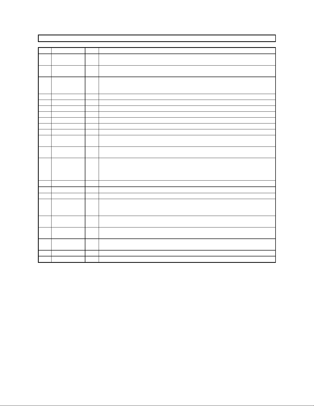
PIN/FUNCTION
No. Pin Name I/O Function
1 SDOS I SDTO Source Select Pin (Note 1)
“L”: Internal ADC output, “H”: DAUX input
2 I2C I Control Mode Select Pin
“L”: 3-wire Serial, “H”: I
2
C Bus
3 SMUTE I Soft Mute Pin (Note 1)
When this pin goes to “H”, soft mute cycle is initialized.
When returning to “L”, the output mute releases.
4 BICK I Audio Serial Data Clock Pin
5 LRCK I Input Channel Clock Pin
6 SDTI1 I DAC1 Audio Serial Data Input Pin
7 SDTI2 I DAC2 Audio Serial Data Input Pin
8 SDTI3 I DAC3 Audio Serial Data Input Pin
9 SDTO O Audio Serial Data Output Pin
10 DAUX I AUX Audio Serial Data Input Pin
11 DFS I Double Speed Sampling Mode Pin (Note 1)
“L”: Normal Speed, “H”: Double Speed
12 NC - No Connect
No internal bonding.
13 DZFE I Zero Input Detect Enable Pin
“L”: mode 7 (disable) at parallel mode,
zero detect mode is selectable by DZFM2-0 bits at serial mode
“H”: mode 0 (DZF1 is AND of all six channels)
14 TVDD 15 DVDD -
Output Buffer Power Supply Pin, 2.7V∼5.5V
Digital Power Supply Pin, 4.5V∼5.5V
16 DVSS - Digital Ground Pin, 0V
17 PDN I Power-Down & Reset Pin
When “L”, the AK4527B is powered-down and the control registers are reset to default
state. If the state of P/S or CAD0-1 changes, then the AK4527B must be reset by PDN.
18 TST I Test Pin
This pin should be connected to DVSS.
19 NC - No Connect
No internal bonding.
20 ADIF I Analog Input Format Select Pin
“H”: Full-differential input, “L”: Single-ended input
21 CAD1 I Chip Address 1 Pin
22 CAD0 I Chip Address 0 Pin
MS0056-E-00 2000/10
- 5 -
Page 6
ASAHI KASEI [AK4527B]
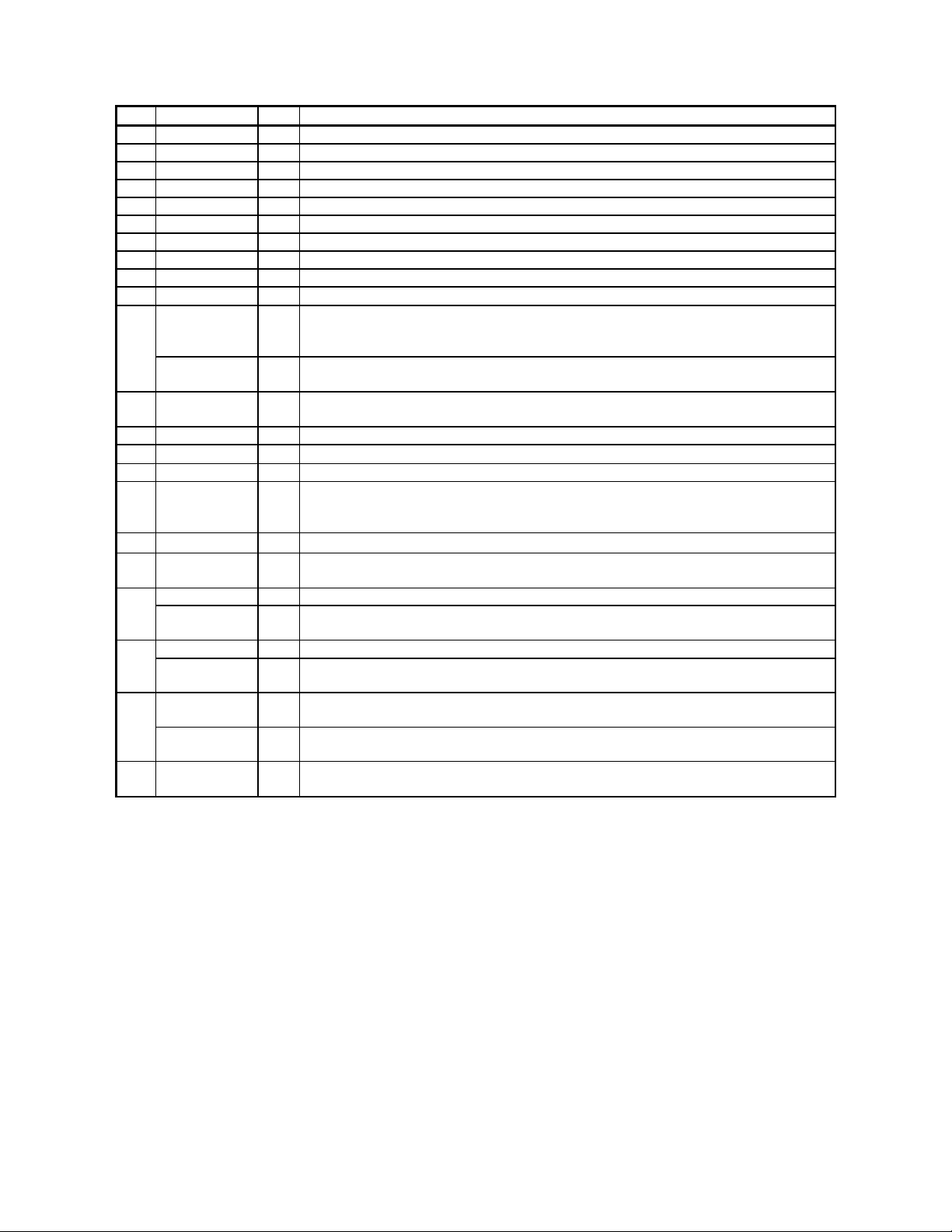
No. Pin Name I/O Function
23 LOUT3 O DAC3 Lch Analog Output Pin
24 ROUT3 O DAC3 Rch Analog Output Pin
25 LOUT2 O DAC2 Lch Analog Output Pin
26 ROUT2 O DAC2 Rch Analog Output Pin
27 LOUT1 O DAC1 Lch Analog Output Pin
28 ROUT1 O DAC1 Rch Analog Output Pin
29 LIN- I Lch Analog Negative Input Pin
30 LIN+ I Lch Analog Positive Input Pin
31 RIN- I Rch Analog Negative Input Pin
32 RIN+ I Rch Analog Positive Input Pin
DZF2 O Zero Input Detect 2 Pin (Note 2)
33
When the input data of the group 1 follow total 8192 LRCK cycles with “0” input data,
this pin goes to “H”.
OVF O Analog Input Overflow Detect Pin (Note 3)
This pin goes to “H” if the analog input of Lch or Rch is overflows.
34 VCOM O Common Voltage Output Pin, AVDD/2
Large external capacitor around 2.2µF is used to reduce power-supply noise.
35 VREFH I Positive Voltage Reference Input Pin, AVDD
36 AVDD -
Analog Power Supply Pin, 4.5V∼5.5V
37 AVSS - Analog Ground Pin, 0V
38 DZF1 O Zero Input Detect 1 Pin (Note 2)
When the input data of the group 1 follow total 8192 LRCK cycles with “0” input data,
this pin goes to “H”.
39 MCLK I Master Clock Input Pin
40 P/S I Parallel/Serial Select Pin
“L”: Serial control mode, “H”: Parallel control mode
DIF0 I Audio Data Interface Format 0 Pin in parallel control mode41
CSN I Chip Select Pin in 3-wire serial control mode
This pin should be connected to DVDD at I
2
C bus control mode
DIF1 I Audio Data Interface Format 1 Pin in parallel control mode42
SCL/CCLK I Control Data Clock Pin in serial control mode
I2C = “L”: CCLK (3-wire Serial), I2C = “H”: SCL (I
LOOP0 I Loopback Mode 0 Pin in parallel control mode
43
2
C Bus)
Enables digital loop-back from ADC to 3 DACs.
SDA/CDTI I/ O Control Data Input Pin in serial control mode
I2C = “L”: CDTI (3-wire Serial), I2C = “H”: SDA (I
2
C Bus)
44 LOOP1 I Loopback Mode 1 Pin (Note 1)
Enables all 3 DAC channels to be input from SDTI1.
Notes: 1. SDOS, SMUTE, DFS, and LOOP1 pins are ORed with register data if P/S = “L”.
2. The group 1 and 2 can be selected by DZFM2-0 bits if P/S = “L” and DZFE = “L”.
3. This pin becomes OVF pin if OVFE bit is set to “1” at serial control mode.
4. All input pins should not be left floating.
MS0056-E-00 2000/10
- 6 -
Page 7

ASAHI KASEI [AK4527B]
ABSOLUTE MAXIMUM RATINGS
(AVSS, DVSS=0V; Note 5)
Parameter Symbol min max Units
Power Supplies Analog
Digital
Output buffer
|AVSS-DVSS| (Note 6)
Input Current (any pins except for supplies) IIN Analog Input Voltage VINA -0.3 AVDD+0.3 V
Digital Input Voltage VIND -0.3 DVDD+0.3 V
Ambient Temperature (power applied) Ta -40 85
Storage Temperature Tstg -65 150
Notes: 5. All voltages with respect to ground.
6. AVSS and DVSS must be connected to the same analog ground plane.
WARNING: Operation at or beyond these limits may result in permanent damage to the device.
Normal operation is not guaranteed at these extremes.
AVDD
DVDD
TVDD
∆GND
-0.3
-0.3
-0.3
-
6.0
6.0
6.0
0.3
±10
V
V
V
V
mA
°C
°C
RECOMMENDED OPERATING CONDITIONS
(AVSS, DVSS=0V; Note 5)
Parameter Symbol min typ max Units
Power Supplies
(Note 7)
Analog
Digital
Output buffer
AVDD
DVDD
TVDD
4.5
4.5
2.7
5.0
5.0
5.0
5.5
5.5
5.5
V
V
V
Notes: 5. All voltages with respect to ground.
7. The power up sequence between AVDD, DVDD and TVDD is not critical.
WARNING: AKM assumes no responsibility for the usage beyond the conditions in this datasheet.
MS0056-E-00 2000/10
- 7 -
Page 8
ASAHI KASEI [AK4527B]
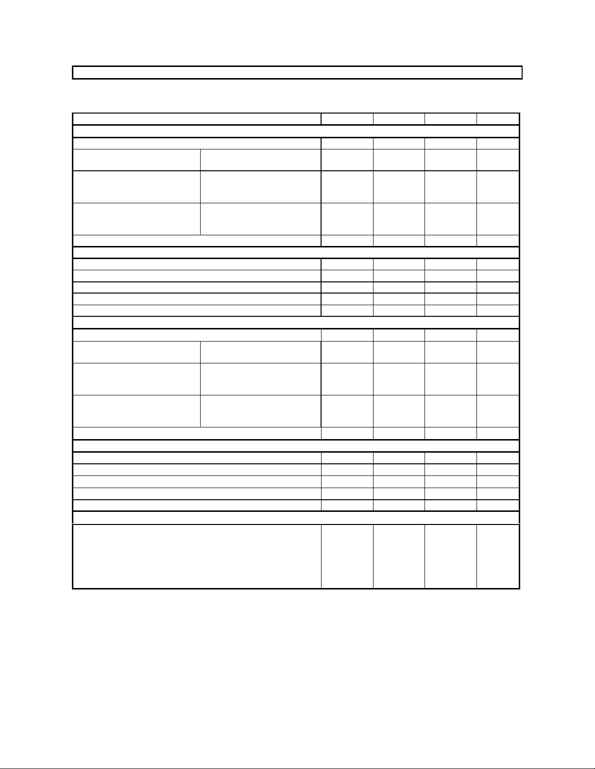
ANALOG CHARACTERISTICS
(Ta=25°C; AVDD, DVDD, TVDD=5V; AVSS, DVSS=0V; VREFH=AVDD; fs=44.1kHz; BICK=64fs;
Signal Frequency=1kHz; 24bit Data; Measurement Frequency=20Hz∼20kHz at fs=44.1kHz, 20Hz~40kHz at fs=96kHz;
unless otherwise specified)
Parameter min typ max Units
ADC Analog Input Characteristics: Differential Inputs; Analog Source Impedance=470Ω
Resolution 24 Bits
S/(N+D) (-0.5dBFS)
(Note 8)
DR (-60dBFS) fs=44.1kHz, A-weighted
S/N (Note 9) fs=44.1kHz, A-weighted
Interchannel Isolation 90 110 dB
DC Accuracy
Interchannel Gain Mismatch 0.2 0. 3 dB
Gain Drift 20 Input Voltage AIN=0.6xVREFH (Note 10) 2.85 3.0 3.15 Vpp
Input Resistance (Note 11) 18 28
Power Supply Rejection (Note 12) 50 dB
DAC Analog Output Characteristics:
Resolution 24 Bits
S/(N+D) fs=44.1kHz
DR (-60dBFS) fs=44.1kHz, A-weighted
S/N (Note 13) fs=44.1kHz, A-weighted
Interchannel Isolation 90 110 dB
DC Accuracy
Interchannel Gain Mismatch 0.2 0.5 dB
Gain Drift 20 Output Voltage AOUT=0.6xVREFH 2.75 3.0 3.25 Vpp
Load Resistance 5
Power Supply Rejection (Note 12) 50 dB
Power Supplies
Power Supply Current
Normal Operation (PDN = “H”)
AVDD
DVDD+TVDD fs=44.1kHz (Note 14)
fs=96kHz
Power-down mode (PDN = “L”) (Note 15)
Notes: 8. In case of single ended input, S/(N+D)=80dB(typ, @AVDD=5V, fs=44.1kHz).
9. S/N measured by CCIR-ARM is 98dB(@fs=44.1kHz).
10. Full scale input for each AIN+/- pin is 1.5Vpp in differential mode.
11. Input resistance is 14kΩ typically at fs=96kHz.
12. PSR is applied to AVDD, DVDD and TVDD with 1kHz, 50mVpp. VREFH pin is held a constant voltage.
13. S/N measured by CCIR-ARM is 102dB(@fs=44.1kHz).
14. DVDD=TBDmA, TVDD=TBDmA(typ).
15. In the power-down mode. All digital input pins including clock pins (MCLK, BICK, LRCK) are held DVSS.
fs=44.1kHz
fs=96kHz
fs=96kHz
fs=96kHz, A-weighted
fs=96kHz
fs=96kHz, A-weighted
fs=96kHz
fs=96kHz
fs=96kHz, A-weighted
fs=96kHz
fs=96kHz, A-weighted
84
94
88
93
94
88
93
80
78
95
88
94
95
88
94
92
-
83
102
96
102
102
96
102
90
88
106
100
106
106
100
106
35
25
35
80
56
40
56
200
dB
dB
dB
dB
dB
dB
dB
dB
ppm/°C
kΩ
dB
dB
dB
dB
dB
dB
dB
dB
ppm/°C
kΩ
mA
mA
mA
µA
MS0056-E-00 2000/10
- 8 -
Page 9

ASAHI KASEI [AK4527B]
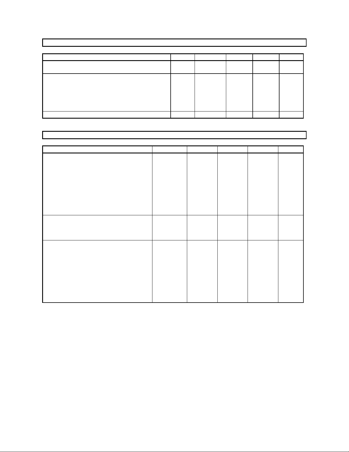
FILTER CHARACTERISTICS
(Ta=25°C; AVDD, DVDD=4.5∼5.5V; TVDD=2.7∼5.5V; fs=44.1kHz; DEM=OFF)
Parameter Symbol min typ max Units
ADC Digital Filter (Decimation LPF):
Passband (Note 16) -0.005dB
-0.02dB
-0.06dB
-6.0dB
Stopband SB 24.34 kHz
Passband Ripple PR
Stopband Attenuation SA 80 dB
Group Delay (Note 17) GD 27.6 1/fs
Group Delay Distortion
ADC Digital Filter (HPF):
Frequency Response (Note 16) -3dB
-0.5dB
-0.1dB
DAC Digital Filter:
Passband (Note 16) -0.1dB
-6.0dB
Stopband SB 24.2 kHz
Passband Ripple PR
Stopband Attenuation SA 56 dB
Group Delay (Note 17) GD 21.9 1/fs
DAC Digital Filter + Analog Filter:
Frequency Response: 0 ∼ 20.0kHz
40.0kHz (Note 18)
PB 0
-
-
-
∆GD
FR 0.9
PB 0
- 22.05
FR
FR
20.02
20.20
22.05
19.76
-
-
-
±0.005
0µs
2.7
6.0
20.0
-
±0.02
±0.2
±0.3
kHz
kHz
kHz
kHz
dB
Hz
Hz
Hz
kHz
kHz
dB
dB
dB
Notes: 16. The passband and stopband frequencies scale with fs.
For example, 20.02kHz at –0.02dB is 0.454 x fs. The reference frequency of these responses is 1kHz.
17. The calculating delay time which occurred by digital filtering. This time is from setting the input of analog
signal to setting the 24bit data of both channels to the output register for ADC.
For DAC, this time is from setting the 20/24bit data of both channels on input register to the output of analog
signal.
18. fs=96kHz.
MS0056-E-00 2000/10
- 9 -
Page 10
ASAHI KASEI [AK4527B]
DC CHARACTERISTICS
(Ta=25°C; AVDD, DVDD=4.5∼5.5V; TVDD=2.7∼5.5V)
Parameter Symbol min typ max Units
High-Level Input Voltage
Low-Level Input Voltage
High-Level Output Voltage
(SDTO pin: Iout=-100µA)
(DZF1, DZF2/OZF pins: Iout=-100µA)
Low-Level Output Voltage
(SDTO, DZF1, DZF2/OZF pins: Iout= 100µA)
(SDA pin: Iout= 3mA)
Input Leakage Current Iin - - ±10 µA
VIH
VIL
VOH
VOH
VOL
VOL
2.2
-
TVDD-0.5
AVDD-0.5
-
-
-
-
-
-
-
-
0.8
0.5
0.4
-
-
-
V
V
V
V
V
V
SWITCHING CHARACTERISTICS
(Ta=25°C; AVDD, DVDD=4.5∼5.5V; TVDD=2.7∼5.5V; CL=20pF)
Parameter Symbol min typ max Units
Master Clock Input
256fsn, 128fsd:
Pulse Width Low
Pulse Width High
384fsn, 192fsd:
Pulse Width Low
Pulse Width High
512fsn, 256fsd:
Pulse Width Low
Pulse Width High
LRCK frequency
Normal Speed Mode
Double Speed Mode
Duty Cycle
Audio Interface Timing
BICK Period
BICK Pulse Width Low
Pulse Width High
LRCK Edge to BICK “↑” (Note 19)
BICK “↑” to LRCK Edge (Note 19)
LRCK to SDTO(MSB)
BICK “↓” to SDTO
SDTI1-3, DAUX Hold Time
SDTI1-3, DAUX Setup Time
fCLK
tCLKL
tCLKH
fCLK
tCLKL
tCLKH
fCLK
tCLKL
tCLKH
fsn
fsd
Duty
tBCK
tBCKL
tBCKH
tLRB
tBLR
tLRS
tBSD
tSDH
tSDS
8.192
27
27
12.288
20
20
16.384
15
15
32
64
45
160
65
65
45
45
40
25
12.288
18.432
24.576
48
96
55
40
40
MHz
ns
ns
MHz
ns
ns
MHz
ns
ns
kHz
kHz
%
ns
ns
ns
ns
ns
ns
ns
ns
ns
Notes: 19. BICK rising edge must not occur at the same time as LRCK edge.
MS0056-E-00 2000/10
- 10 -
Page 11

ASAHI KASEI [AK4527B]
0.025*1/fs
Parameter Symbol min typ max Units
Control Interface Timing (3-wire Serial mode):
CCLK Period
CCLK Pulse Width Low
Pulse Width High
CDTI Setup Time
CDTI Hold Time
CSN “H” Time
CSN “↓” to CCLK “↑”
CCLK “↑” to CSN “↑”
Rise Time of CSN
Fall Time of CSN
Rise Time of CCLK
Fall Time of CCLK
tCCK
tCCKL
tCCKH
tCDS
tCDH
tCSW
tCSS
tCSH
tR1
tF1
tR2
tF2
200
80
80
40
40
50
50
20
20
20
20
ns
ns
ns
ns
ns
ns
ns
ns
ns
ns
ns
ns
Control Interface Timing (I2C Bus mode):
SCL Clock Frequency
Bus Free Time Between Transmissions
Start Condition Hold Time (prior to first clock pulse)
Clock Low Time
Clock High Time
Setup Time for Repeated Start Condition
SDA Hold Time from SCL Falling (Note 20)
SDA Setup Time from SCL Rising
Rise Time of Both SDA and SCL Lines
Fall Time of Both SDA and SCL Lines
Setup Time for Stop Condition
Pulse Width of Spike Noise Suppressed by Input Filter
fSCL
tBUF
tHD:STA
tLOW
tHIGH
tSU:STA
tHD:DAT
tSU:DAT
tR
tF
tSU:STO
tSP
-
4.7
4.0
4.7
4.0
4.7
0
0.25
-
-
4.0
0
100
-
-
-
-
-
-
-
1.0
0.3
-
50
kHz
µs
µs
µs
µs
µs
µs
µs
µs
µs
µs
ns
Power-down & Reset Timing
PDN Pulse Width (Note 21)
PDN “↑” to SDTO valid (Note 22)
tPD
tPDV
150
522
ns
1/fs
Notes: 20. Data must be held for sufficient time to bridge the 300 ns transition time of SCL.
21. The AK4527B can be reset by bringing PDN “L” to “H” upon power-up.
22. These cycles are the number of LRCK rising from PDN rising.
2
23. I
C is a registered trademark of Philips Semiconductors.
Purchase of Asahi Kasei Microsystems Co., Ltd I
2
I
C patent to use the components in the I2C system, provided the system conform to the I2C
2
C components conveys a license under the Philips
specifications defined by Philips.
MS0056-E-00 2000/10
- 11 -
Page 12

ASAHI KASEI [AK4527B]
n Timing Diagram
1/fCLK
MCLK
LRCK
BICK
LRCK
BICK
tBLR
tCLKH
tBCKH
VIH
VIL
tCLKL
1/fs
VIH
VIL
tBCK
VIH
VIL
tBCKL
Clock Timing
VIH
VIL
tLRB
VIH
VIL
SDTO
SDTI
tLRS
tSDS
tSDH
Audio Interface Timing
tBSD
50%TVDD
VIH
VIL
MS0056-E-00 2000/10
- 12 -
Page 13

ASAHI KASEI [AK4527B]
CSN
CCLK
CDTI
CSN
CCLK
CDTI
tCSS
C1 C0 R /W A4
tCCKL tCCKH
tCDS tCDH
WRITE Command Input Timing (3-wire Serial mode)
tCSW
D3 D2 D1 D0
VIH
VIL
VIH
VIL
VIH
VIL
VIH
VIL
tCSH
VIH
VIL
VIH
VIL
WRITE Data Input Timing (3-wire Serial mode)
SDA
tLOW
tBUF
SCL
tHD:STA
Stop Start Start Stop
tR
tHD:DAT tSU:DAT tSU:STA
tHIGH
tF
I2C Bus mode Timing
tPD
PDN
tPDV
SDTO
Power-down & Reset Timing
VIH
VIL
tSP
VIH
VIL
tSU:STO
VIH
VIL
50%TVDD
MS0056-E-00 2000/10
- 13 -
Page 14

ASAHI KASEI [AK4527B]
OPERATION OVERVIEW
n System Clock
The external clocks, which are required to operate the AK4527B, are MCLK, LRCK and BICK. There are two methods to
set MCLK frequency. In Manual Setting Mode (ACKS = “0”: Default), the sampling speed is set by DFS (Table 1). The
frequency of MCLK at each sampling speed is set automatically. (Table 2, 3). In Auto Setting Mode (ACKS = “1”), as
MCLK frequency is detected automatically (Table 4), and the internal master clock becomes the appropriate frequency
(Table 5), it is not necessary to set DFS.
MCLK should be synchronized with LRCK but the phase is not critical. External clocks (MCLK, BICK) should always be
present whenever the AK4527B is in normal operation mode (PDN = “H”). If these clocks are not provided, the
AK4527B may draw excess current because the device utilizes dynamic refreshed logic internally. If the external clocks
are not present, the AK4527B should be in the power-down mode (PDN = “L”) or in the reset mode (RSTN = “0”). After
exiting reset at power-up etc., the AK4527B is in the power-down mode until MCLK and LRCK are input.
DFS Sampling Speed (fs)
0 Normal Speed Mode 32kHz~48kHz
1 Double Speed Mode 64kHz~96kHz
Table 1. Sampling Speed (Manual Setting Mode)
Default
LRCK MCLK (MHz) BICK (MHz)
fs 256fs 384fs 512fs 64fs
32.0kHz 8.1920 12.2880 16.3840 2.0480
44.1kHz 11.2896 16.9344 22.5792 2.8224
48.0kHz 12.2880 18.4320 24.5760 3.0720
Table 2. System Clock Example (Normal Speed Mode @Manual Setting Mode)
LRCK MCLK (MHz) BICK (MHz)
fs 128fs 192fs 256fs 64fs
88.2kHz 11.2896 16.9344 22.5792 5.6448
96.0kHz 12.2880 18.4320 24.5760 6.1440
Table 3. System Clock Example (Double Speed Mode @Manual Setting Mode)
(Note: At double speed mode(DFS = “1”), 128fs and 192fs are not available for ADC.)
MCLK Sampling Speed
512fs Normal
256fs Double
Table 4. Sampling Speed (Auto Setting Mode)
MS0056-E-00 2000/10
- 14 -
Page 15

ASAHI KASEI [AK4527B]
LRCK MCLK (MHz)
fs 256fs 512fs
32.0kHz - 16.3840
44.1kHz - 22.5792
48.0kHz - 24.5760
88.2kHz 22.5792 -
96.0kHz 24.5760 -
Table 5. System Clock Example (Auto Setting Mode)
Sampling
Speed
Normal
Double
n De-emphasis Filter
The AK4527B includes the digital de-emphasis filter (tc=50/15µs) by IIR filter. This filter corresponds to three sampling
frequencies (32kHz, 44.1kHz, 48kHz). De-emphasis of each DAC can be set individually by register data of DEMA1-C0
(DAC1: DEMA1-0, DAC2: DEMB1-0, DAC3: DEMC1-0, see “Register Definitions”).
Mode Sampling Speed DEM1 DEM0 DEM
0 Normal Speed 0 0 44.1kHz
1 Normal Speed 0 1 OFF
2 Normal Speed 1 0 48kHz
3 Normal Speed 1 1 32kHz
4 Double Speed 0 0 OFF
5 Double Speed 0 1 OFF
6 Double Speed 1 0 OFF
7 Double Speed 1 1 OFF
Default
Table 6. De-emphasis control
n Digital High Pass Filter
The ADC has a digital high pass filter for DC offset cancel. The cut-off frequency of the HPF is 0.9Hz at fs=44.1kHz and
also scales with sampling rate (fs).
n Audio Serial Interface Format
Four serial data modes can be selected by the DIF0 and DIF1 pins (P/S = “H”) or bits (P/S = “L”) as shown in Table 7. In
all modes the serial data is MSB-first, 2’s compliment format. The SDTO is clocked out on the falling edge of BICK and
the SDTI/DAUX are latched on the rising edge of BICK.
Figures 1∼4 shows the timing at SDOS = “L”. In this case, the SDTO outputs the ADC output data. When SDOS = “H”,
the data input to DAUX is converted to SDTO’s format and output from SDTO. Mode 2 and mode 3 in SDTI/DAUX
input formats can be used for 16-20bit data by zeroing the unused LSBs.
Mode DIF1 DIF0 SDTO SDTI1-3, DAUX LRCK
0 0 0 24bit, MSB justified 20bit, LSB justified H/L
1 0 1 24bit, MSB justified 24bit, LSB justified H/L
2 1 0 24bit, MSB justified 24bit, MSB justified H/L
3 1 1 24bit, IIS (I2S) 24bit, IIS (I2S) L/H
Table 7. Audio data formats
Default
MS0056-E-00 2000/10
- 15 -
Page 16

ASAHI KASEI [AK4527B]
(
)
)
)
(
)
)
)
(
)
SDTO(o)
)
(
)
)
)
LRCK
0 1 2 12 13 14 24 25 31 0 1 2 12 13 14 24 25 31 0231
64fs
BICK
SDTO(o
SDTI(i
LRCK
BICK
SDTO(o
SDTI(i
LRCK
BICK
64fs
64fs
22 0 23 22 12 11 10 0 23
Don’t Care Don’t Care
SDTO-23:MSB, 0:LSB; SDTI-19:MSB, 0:LSB
12 11 10
118 019 8 7 118 019 8 7
Lch Data Rch Data
Figure 1. Mode 0 Timing
0 1 2 8 9 10 24 25 31 0 1 2 8 9 10 24 25 31 0231
22 0 23 22 16 15 14 0 23
Don’t Care Don’t Care
23:MSB, 0:LSB
16 15 14
122 023 8 7 122 023 8 7
Lch Data Rch Data
Figure 2. Mode 1 Timing
0 1 2 18192021 31 0 1 2 0231
28 29 30
19 20 21 31
28 29 30
SDTI(i
LRCK
BICK
SDTO(o
SDTI(i
64fs
22 1 23 22 23
2223 0 2223
23:MSB, 0:LSB
2
21
0
Don’t Care
2
21
Lch Data Rch Data
1
0
0
Don’t Care
23
Figure 3. Mode 2 Timing
0 1 2 3 23 24 25 26 0 0 1
23 22 1
2223 0
23:MSB, 0:LSB
2
21
0
Don’t Care
Lch Data Rch Data
3129 30
2 3 23 24 25 26 03129 30
1
23 22 1
2223 0 Don’t Care
2
21
0
Figure 4. Mode 3 Timing
MS0056-E-00 2000/10
- 16 -
Page 17

ASAHI KASEI [AK4527B]
n
Overflow Detection
The AK4527B has overflow detect function for analog input. Overflow detection is enabled when OVFE bit is set to “1”
at serial control mode. OVF pin goes to “H” if analog input of Lch or Rch overflows. OVF output for overflowed analog
input has the same group delay as ADC (GD=27.6/fs=626µ s@fs=44.1kHz).
OVF is “L” for 522/fs(=11.8ms@fs=44.1kHz) after PDN = “↑”, and then overflow detection is enabled.
n Zero detection
The AK4527B has two pins for zero detect flag outputs. Channel grouping can be selected by DZFM2-0 bits if P/S = “L”
and DZFE = “L” (table 8). DZF1 pin corresponds to the group 1 channels and DZF2 pin corresponds to the group 2
channels. However DZF2 pin becomes OVF pin if OVFE bit is set to “1”. Zero detection mode is set to mode 0 if DZFE=
“H” regardless of P/S pin. DZF1 is AND of all six channels and DZF2 is disabled (“L”) at mode 0. Table 9 shows the
relation of P/S, DZFE, OVFE and DZF.
When the input data of all channels in the group 1(group 2) are continuously zeros for 8192 LRCK cycles, DZF1(DZF2)
pin goes to “H”. DZF1(DZF2) pin immediately goes to “L” if input data of any channels in t he group 1(group 2) is not
zero after going DZF1(DZF2) “H”.
Mode
0 0 0 0 DZF1 DZF1 DZF1 DZF1 DZF1 DZF1
1 0 0 1 DZF1 DZF1 DZF1 DZF1 DZF1 DZF2
2 0 1 0 DZF1 DZF1 DZF1 DZF1 DZF2 DZF2
3 0 1 1 DZF1 DZF1 DZF1 DZF2 DZF2 DZF2
4 1 0 0 DZF1 DZF1 DZF2 DZF2 DZF2 DZF2
5 1 0 1 DZF1 DZF2 DZF2 DZF2 DZF2 DZF2
6 1 1 0 DZF2 DZF2 DZF2 DZF2 DZF2 DZF2
7 1 1 1 disable (DZF1=DZF2 = “L”)
P/S pin DZFE pin OVFE bit DZF mode DZF1 pin DZF2/OVF pin
“L” (serial mode)
DZFM AOUT
2 1 0 L1 R1 L2 R2 L3 R3
Table 8. Zero detect control
“L” disable Mode 7 “L” “L”“H” (parallel mode)
“H” disable Mode 0 AND of 6ch “L”
“0” Selectable Selectable Selectable“L”
“1” Selectable Selectable OVF output
“H”
“0” Mode 0 AND of 6ch “L”
“1” Mode 0 AND of 6ch OVF output
Table 9. DZF1-2 pins outputs
Default
MS0056-E-00 2000/10
- 17 -
Page 18

ASAHI KASEI [AK4527B]
n
Digital Attenuator
AK4527B has channel-independent digital attenuator (256 levels, 0.5dB step). Attenuation level of each channel can be
set by each ATT7-0 bits (table 10).
ATT7-0 Attenuation Level
00H 0dB
01H -0.5dB
02H -1.0dB
::
FDH -126.5dB
FEH -127.0dB
FFH
Table 10. Attenuation level of digital attenuator
The transition between set values is soft transition of 7425 levels. It takes 7424/fs (168ms@fs=44.1kHz) from 00H(0dB)
to FFH(MUTE). If PDN pin goes to “L”, the ATTs are initialized to 00H. The ATTs are 00H when RSTN = “0” . When
RSTN return to “1”, the ATTs fade to their current value. Digital attenuator is independent of soft mute function.
MUTE (-∞)
Default
MS0056-E-00 2000/10
- 18 -
Page 19

ASAHI KASEI [AK4527B]
n Soft mute operation
Soft mute operation is performed at digital domain. When the SMUTE pin goes to “H”, the output signal is attenuated by
-∞ during 1024 LRCK cycles. When the SMUTE pin is returned to “L”, the mute is cancelled and the output attenuation
gradually changes to 0dB during 1024 LRCK cycles. If the soft mute is cancelled within 1024 LRCK cycles after starting
the operation, the attenuation is discontinued and returned to 0dB. The soft mute is effective for changing the signal
source without stopping the signal transmission.
SMUTE
Attenuation
AOUT
0dB
-
1024/fs
(1)
∞
GD
(2)
1024/fs
(3)
GD
(4)
DZF1,2
Notes:
(1) The output signal is attenuated by -∞ during 1024 LRCK cycles (1024/fs).
(2) Analog output corresponding to digital input have the group delay (GD).
(3) If the soft mute is cancelled within 1024 LRCK cycles, the attenuation is discontinued and returned to 0dB.
(4) When the input data of all channels in the group are continuously zeros for 8192 LRCK cycles, DZF pin
corresponding to the group goes to “H”. DZF pin immediately goes to “L” if input data of any channel in the group
is not zero after going DZF “H”.
Figure 5. Soft mute and zero detection
8192/fs
n System Reset
The AK4527B should be reset once by bringing PDN = “L” upon power-up. The AK4527B is powered up and the
internal timing starts clocking by LRCK “↑” after exiting reset and power down state by MCLK. The AK4527B is in the
power-down mode until MCLK and LRCK are input.
MS0056-E-00 2000/10
- 19 -
Page 20

ASAHI KASEI [AK4527B]
n Power-Down
The ADC and DACs of AK4527B are placed in the power-down mode by bringing PDN “L” and both digital filters are
reset at the same time. PDN “L” also reset the control registers to their default values. In the power-down mode, the
analog outputs go to VCOM voltage and DZF1-2 pins go to “L”. This reset should always be done after power-up. In case
of the ADC, an analog initialization cycle starts after exiting the power-down mode. Therefore, the output data, SDTO
becomes available after 522 cycles of LRCK clock. In case of the DAC, an analog initialization cycle starts after exiting
the power-down mode. The analog outputs are VCOM voltage during the initialization. Figure 6 shows the power-up
sequence.
The ADC and DACs can be powered-down individually by PWADN and PWDAN bits. In this case, the internal register
values are not initialized. When PWADN = “0”, SDTO goes to “L”. When PWDAN = “0”, the analog outputs go to
VCOM voltage and DZF1-2 pins go to “H”. Because some click noise occurs, the analog output should muted externally
if the click noise influences system application.
PDN
ADC Internal
State
DAC Internal
State
ADC In
(Analog)
ADC Out
(Digital)
DAC In
(Digital)
DAC Out
(Analog)
Clock In
MCLK,LRCK,SCLK
DZF1/DZF2
External
Mute
Normal Operation Power-down Init Cycle Normal Operation
Normal Operation
GD
GD
(9)
Power-down Normal Operation
(3)
(4)
“0”data
“0”data
(3)
(6) (6)
(7)
Don’t care
10∼11/fs (10)
(8)
Mute ON
522/fs
516/fs
Init Cycle
(1)
(2)
GD
(5)
GD
Notes:
(1) The analog part of ADC is initialized after exiting the power-down state.
(2) The analog part of DAC is initialized after exiting the power-down state.
(3) Digital output corresponding to analog input and analog output corresponding to digital input have the group delay
(GD).
(4) ADC output is “0” data at the power-down state.
(5) Click noise occurs at the end of initialization of the analog part. Please mute the digital output externally if the click
noise influences system application. Required muting time depends on the configuration of the input buffer circuits.
Figure 12,13: 1s
Figure 14,15: 200ms
(6) Click noise occurs at the falling edge of PDN and at 512/fs after the rising edge of PDN.
(7) When the external clocks (MCLK, BICK and LRCK) are stopped, the AK4527B should be in the power-down
mode.
(8) DZF pins are “L” in the power-down mode (PDN = “L”).
(9) Please mute the analog output externally if the click noise (6) influences system application.
(10) DZF= “L” for 10∼11/fs after PDN= “↑”.
Figure 6. Power-down/up sequence example
MS0056-E-00 2000/10
- 20 -
Page 21

ASAHI KASEI [AK4527B]
n Reset Function
When RSTN = “0”, ADC and DACs are powered-down but the internal register are not initialized. The analog outputs go
to VCOM voltage, DZF1-2 pins go to “H” and SDTO pin goes to “L”. Because some click noise occurs, the analog output
should muted externally if the click noise influences system application. Figure 7 shows the power-up sequence.
RSTN bit
Internal
RSTN bit
ADC Internal
State
Normal Operation
Digital Block Power-down
1~2/fs (9)4~5/fs (9)
(1)
516/fs
Init Cycle
Normal Operation
DAC Internal
State
ADC In
(Analog)
ADC Out
(Digital)
DAC In
(Digital)
DAC Out
(Analog)
Clock In
MCLK,LRCK,SCLK
DZF1/DZF2
Normal Operation
Digital Block Power-down
(2)
GD GD
(3)
“0”data
“0”data
(2)
GD GD
(6) (6)
(5)
(7)
Don’t care
4∼5/fs (8)
Normal Operation
(4)
Notes:
(1) The analog part of ADC is initialized after exiting the reset state.
(2) Digital output corresponding to analog input and analog output corresponding to digital input have the group delay
(GD).
(3) ADC output is “0” data at the power-down state.
(4) Click noise occurs when the internal RSTN bit becomes “1”. Please mute the digital output externally if the click
noise influences system application. Required muting time depends on the configuration of the input buffer circuits.
Figure 12,13: 1s
Figure 14,15: 200ms
(5) The analog outputs go to VCOM voltage.
(6) Click noise occurs a t 4∼5/fs after RSTN bit becomes “0”, and occurs at 1∼2/fs after RSTN bit becomes “1”. This
noise is output even if “0” data is input.
(7) The external clocks (MCLK, BICK and LRCK) can be stopped in the reset mode. When exiting the reset mode, “1”
should be written to RSTN bit after the external clocks (MCLK, BICK and LRCK) are fed.
(8) DZF pins go to “H” when the RSTN bit becomes “0”, and go to “L” at 6~7/fs a f t e r RSTN bit becomes “1”.
(9) There is a delay, 4~5/fs from RSTN bit “0” to the internal RSTN bit “0 ”.
Figure 7. Reset sequence example
MS0056-E-00 2000/10
- 21 -
Page 22

ASAHI KASEI [AK4527B]
D0
n Serial Control Interface
The AK4527B can control its functions via registers. Internal registers may be written by 2 types of control mode. The
chip address is determined by the state of the CAD0 and CAD1 inputs. PDN = “L” initializes the registers to their default
values. Writing “0” to the RSTN bit can initialize the internal timing circuit. But in this case, the register data is not be
initialized. When the state of P/S pin is changed, the AK4527B should be reset by PDN pin.
* Writing to control register is invalid when PDN = “L” or the MCLK is not fed.
* AK4527B does not support the read command.
(1) 3-wire Serial Control Mode (I2C = “L”)
Internal registers may be written to the 3 wire µP interface pins (CSN,CCLK and CDTI). The data on this interface
consists of Chip address (2bits, CAD0/1), Read/Write (1bit, Fixed to “1”; Write only), Register address (MSB first,
5bits) and Control data (MSB first, 8bits). Address and data is clocked in on the rising edge of CCLK and data is
clocked out on the falling edge. For write operations, data is latched after a low-to-high transition of CSN. The clock
speed of CCLK is 5MHz(max). The CSN pins should be held to “H” except for access.
CSN
0 1234567
8 9 10 11 12 13 14 15
CCLK
CDTI
C1
D4D5D6D7A1A2A3A4R/WC0 A0
D1D2D3
C1-C0: Chip Address (C1=CAD1, C0=CAD0)
R/W: Read/Write (Fixed to “1” : Write only)
A4-A0: Register Address
D7-D0: Control Data
Figure 8. 3-wire Serial Control I/F Timing
2
(2) I
C Bus Control Mode (I2C = “H”)
Internal registers may be written to I
2
C Bus interface pins: SCL & SDA. The data on this interface consists of Chip
address (2bits, CAD0/1), Read/Write (1bit, Fixed to “0”; Write only), Register address (MSB first, 5bits) and
Control data (MSB first, 8bits). Address and data is clocked in on the rising edge of SCL and data is clocked out on
the falling edge. Data can be written after a high-to-low transition of SDA when SCL is “H”(start condition), and is
latched after a low-to-high transition of SDA when SCL is “H”(stop condition). The clock speed of SCL is
100kHz(max). The CSN pin should be connected to DVDD at I
2
C Bus control mode. The AK4527B does not have a
register address auto increment capability.
SDA
0 0100
R/W
ACK
C1 C0 0 0 0 A4 A3 A2 A1 A0 D7 D6 D5 D4 D3 D2 D1 D0
ACK
ACK
SCL
Start
Stop
C1-C0: Chip Address (C1=CAD1, C0=CAD0)
R/W: Read/Write (Fixed to “0” : Write only)
A4-A0: Register Address
D7-D0: Control Data
ACK: Acknowledge
Figure 9. I
2
C-bus Control I/F Timing
MS0056-E-00 2000/10
- 22 -
Page 23

ASAHI KASEI [AK4527B]
n Mapping of Program Registers
Addr Register Name D7 D6 D5 D4 D3 D2 D1 D0
00H Control 1 0 0 0 0 DIF1 DIF0 0
SMUTE
01H Control 2 0 0 LOOP1 LOOP0 SDOS DFS ACKS 0
02H LOUT1 Volume Control ATT7 ATT6 ATT5 ATT4 ATT3 ATT2 ATT1 ATT0
03H ROUT1 Volume Control ATT7 ATT6 ATT5 ATT4 ATT3 ATT2 ATT1 ATT0
04H LOUT2 Volume Control ATT7 ATT6 ATT5 ATT4 ATT3 ATT2 ATT1 ATT0
05H ROUT2 Volume Control ATT7 ATT6 ATT5 ATT4 ATT3 ATT2 ATT1 ATT0
06H LOUT3 Volume Control ATT7 ATT6 ATT5 ATT4 ATT3 ATT2 ATT1 ATT0
07H ROUT3 Volume Control ATT7 ATT6 ATT5 ATT4 ATT3 ATT2 ATT1 ATT0
08H De-emphasis
0 0 DEMA1 DEMA0 DEMB1 DEMB0 DEMC1 DEMC0
09H Reset 0 0 0 0 0 0 0 RSTN
0AH Zero detect
OVFE 0
DZFM2 DZFM1 DZFM 0 PWVRN PWADN PWDAN
Note: For addresses from 0BH to 1FH, data is not written.
When PDN goes to “L”, the registers are initialized to their default values.
When RSTN bit goes to “0”, the internal timing is reset and DZF1-2 pins go to “H”, but registers are not initialized
to their default values.
SMUTE, DFS, SDOS and LOOP1 are ORed with pins.
MS0056-E-00 2000/10
- 23 -
Page 24

ASAHI KASEI [AK4527B]
n
Register Definitions
Addr Register Name D7 D6 D5 D4 D3 D2 D1 D0
00H Control 1 0 0 0 0 DIF1 DIF0 0
default 0 0 0 0 1 0 0 0
SMUTE: Soft Mute Enable
0: Normal operation
1: All DAC outputs soft-muted
Register bit of SMUTE is ORed with the SMUTE pin if P/S = “L” .
DIF1-0: Audio Data Interface Modes (see table 7.)
Initial: “10”, mode 2
Addr Register Name D7 D6 D5 D4 D3 D2 D1 D0
01H Control 2 0 0 LOOP1 LOOP0 SDOS DFS ACKS 0
default 0 0 0 0 0 0 0 0
ACKS: Master Clock Frequency Auto Setting Mode Enable
0: Disable, Manual Setting Mode
1: Enable, Auto Setting Mode
Master clock frequency is detected automatically at ACKS bit “1”. In this case, the setting of DFS are
ignored. When this bit is “0”, DFS sets the sampling speed mode.
SMUTE
DFS: Sampling speed mode (see table 1.)
0: Normal speed
1: Double speed
Register bit of DFS is ORed with DFS pin if P/S = “L”. The setting of DFS are ignored at ACKS bit “1”.
SDOS: SDTO source select
0: ADC
1: DAUX
Register bit of SDOS is ORed with SDOS pin if P/S = “L”.
LOOP1-0: Loopback mode enable
00: Normal (No loop back)
01: LIN → LOUT1, LOUT2, LOUT3
RIN → ROUT1, ROUT2, ROUT3
The digital ADC output (DAUX input if SDOS = “1”) is connected to the digital DAC input. In this
mode, the input DAC data to SDTI1-3 is ignored. The audio format of SDTO at loopback mode
becomes mode 2 at mode 0, and mode 3 at mode 1, respectively.
10: SDTI1(L) → SDTI2(L), SDTI3(L)
SDTI1(R) → SDTI2(R), SDTI3(R)
In this mode the input DAC data to SDTI2-3 is ignored.
11: N/A
Register bit of LOOP1 is ORed with LOOP1 pin if P/S = “L”.
MS0056-E-00 2000/10
- 24 -
Page 25

ASAHI KASEI [AK4527B]
Addr Register Name D7 D6 D5 D4 D3 D2 D1 D0
02H LOUT1 Volume Control ATT7 ATT6 ATT5 ATT4 ATT3 ATT2 ATT1 ATT0
03H ROUT1 Volume Control ATT7 ATT6 ATT5 ATT4 ATT3 ATT2 ATT1 ATT0
04H LOUT2 Volume Control ATT7 ATT6 ATT5 ATT4 ATT3 ATT2 ATT1 ATT0
05H ROUT2 Volume Control ATT7 ATT6 ATT5 ATT4 ATT3 ATT2 ATT1 ATT0
06H LOUT3 Volume Control ATT7 ATT6 ATT5 ATT4 ATT3 ATT2 ATT1 ATT0
07H ROUT3 Volume Control ATT7 ATT6 ATT5 ATT4 ATT3 ATT2 ATT1 ATT0
Default 0 0 0 0 0 0 0 0
ATT7-0: Attenuation Level (see table 9.)
Addr Register Name D7 D6 D5 D4 D3 D2 D1 D0
08H De-emphasis
0 0 DEMA1 DEMA0 DEMB1 DEMB0 DEMC1 DEMC0
Default 0 0 0 1 0 1 0 1
DEMA1-0: De-emphasis response control for DAC1 data on SDTI1 (see table 6.)
Initial: “01”, OFF
DEMB1-0: De-emphasis response control for DAC2 data on SDTI2 (see table 6.)
Initial: “01”, OFF
DEMC1-0: De-emphasis response control for DAC3 data on SDTI3 (see table 6.)
Initial: “01”, OFF
MS0056-E-00 2000/10
- 25 -
Page 26

ASAHI KASEI [AK4527B]
Addr Register Name D7 D6 D5 D4 D3 D2 D1 D0
09H Clock mode 0 0 0 0 0 0 0 RSTN
Default 0 0 0 0 0 0 0 1
RSTN: Internal timing reset
0: Reset. DZF1-2 pins go to “H”, but registers are not initialized.
1: Normal operation
Addr Register Name D7 D6 D5 D4 D3 D2 D1 D0
0AH Zero detect
OVFE 0 DZFM2 DZFM1 DZFM0 PWVRN PWADN PWDAN
Default 0 01111 1 1
PWDAN: Power-down control of DAC1-3
0: Power-down
1: Normal operation
PWADN: Power-down control of ADC
0: Power-down
1: Normal operation
PWVRN: Power-down control of reference voltage
0: Power-down
1: Normal operation
DZFM2-0: Zero detect mode select (see table 8.)
Initial: “111”, disable
OVFE: Overflow detection enable
0: Disable, pin#33 becomes DZF2 pin.
1: Enable, pin#33 becomes OVF pin.
MS0056-E-00 2000/10
- 26 -
Page 27

ASAHI KASEI [AK4527B]
K
S
H
D
N
SYSTEM DESIGN
Figure 10 shows the system connection diagram. An evaluation board is available which demonstrates application
circuits, the optimum layout, power supply arrangements and measurement results.
Condition: TVDD=5V, 3-wire serial control mode, CAD1-0 = “00”, Full-differential input
Analog 5V
+
10u
uP
Digital
Audio
Source
(DIR)
Audio
DSP
(MPEG/
AC3)
Power-down
control
2
3
4
5
6
7
8
9
10
11
SDOS1
I2C
SMUTE
BICK
LRCK
SDTI1
SDTI2
SDTI3
SDTO
DAUX
DFS
44
43
CDTI
LOOP1
NC
DZFE
12
13
42
CCL
TVDD
14
+
41
CS
DVDD
15
40
39
P/S
MCLK
AK4527B
PDN
DVSS
16
17
0.1u
10u
+
0.1u
38
37
36
DZF1
AVS
AVD
TSTNCADIF
18
19
20
2.2u
0.1u
35
VREF
CAD1
21
5
34
VCOM
DZF2 33
RIN+
RINLIN+
LINROUT1
LOUT1
ROUT2
LOUT2
ROUT3
LOUT3
CAD0
22
32
31
30
29
28
27
26
25
24
23
1n
1n
470
470
470
470
MUTE
MUTE
MUTE
MUTE
MUTE
MUTE
Analog GroundDigital Ground
Figure 10. Typical Connection Diagram
MS0056-E-00 2000/10
- 27 -
Page 28

ASAHI KASEI [AK4527B]
LOOP0/SDA/CDTI
K
DZFE
Analog GroundDigital Ground
4443424140393837363534
P/S
DZF1
AVSS
MCL
AVDD
VCOM
VREFH
DZF2/OVF
RINLIN+
LINROUT1
LOUT1
ROUT2
LOUT2
ROUT3
LOUT3
CAD1
CAD0
33
31
30
29
28
27
26
25
24
23
System
Controller
LOOP1
3
4
5
6
7
8
9
10
11
SDOS1
I2C
SMUTE
BICK
LRCK
SDTI1
SDTI2
SDTI3
SDTO
DAUX
DFS
DIF0/CSN
DIF1/SCL/CCLK
AK4527B
NC
TVDD
DVSS
DVDD
1213141516171819202122
TSTNCADIF
PDN
Figure 11. Ground Layout
Note: AVSS and DVSS must be connected to the same analog ground plane.
1. Grounding and Power Supply Decoupling
The AK4527B requires careful attention to power supply and grounding arrangements. AVDD and DVDD are usually
supplied from analog supply in system. Alternatively if AVDD and DVDD are supplied separately, the power up
sequence is not critical. AVSS and DVSS of the AK4527B must be connected to analog ground plane. System analog
ground and digital ground should be connected together near to where the supplies are brought onto the printed circuit
board. Decoupling capacitors should be as near to the AK4527B as possible, with the small value ceramic capacitor being
the nearest.
2. Voltage Reference Inputs
The voltage of VREFH sets the analog input/output range. VREFH pin is normally connected to AVDD with a 0.1µF
ceramic capacitor. VCOM is a signal ground of this chip. An electrolytic capacitor 2.2µF parallel with a 0.1µF ceramic
capacitor attached to VCOM pin eliminates the effects of high frequency noise. No load current may be drawn from
VCOM pin. All signals, especially clocks, should be kept away from the VREFH and VCOM pins in order to avoid
unwanted coupling into the AK4527B.
3. Analog Inputs
The ADC inputs are differential. Figures 12 and 13 are circuit examples which analog signal is input by single end
(ADIF= “L”). The signal can be input from either positive or negative input and the input signal range scales with the
supply voltage and nominally 0.6 x VREFH Vpp. In case of single ended input, the distortion around full scale degrades
compared with differential input (ADIF= “H”). Figures 14 and 15 are circuit examples which analog signal is input to
both positive and negative input and the input signal range scales with the supply voltage and nominally 0.3 x VREFH
Vpp. The AK4527B can accept input voltages from AVSS to AVDD. The ADC output data format is 2’s complement.
The output code is 7FFFFFH(@24bit) for input above a positive full scale and 800000H(@24bit) for input below a
negative fill scale. The ideal code is 000000H(@24bit) with no input signal. The DC offset is removed by the internal
HPF.
The AK4527B samples the analog inputs at 64fs. The digital filter rejects noise above the stop band except for multiples
of 64fs. A simple RC filter (fc=150kHz) may be used to attenuate any noise around 64fs and most audio signals do not
have significant energy at 64fs.
MS0056-E-00 2000/10
- 28 -
Page 29

ASAHI KASEI [AK4527B]
4.7k
BIAS
4.7k
BIAS
AK4527B
RIN+
RIN-
LIN+
LIN-
2.2nF 470
32
31
30
29
470
Same circuit
4.7k
4.7k
AVDD
22µ
0.1µ
Signal
BIAS
+
10µ
Figure 12. Single End Input Example (ADIF= “L”; Not using op-amp)
AK4527B
RIN+
RIN-
LIN+
LIN-
2.2nF 470
32
31
30
29
NJM2100
Vop=AVDD=5V
470
3.0Vpp
Same circuit
Vop
-
+
Figure 13. Single End Input Example (ADIF= “L”; Using op-amp)
4.7k
4.7k
10k
AVDD
0.1µ
3.0Vpp
22µ
+
Signal
6.4Vpp
10µ
AK4527B
RIN+
RIN-
LIN+
LIN-
1.5Vpp
1nF 470
32
31
30
29
470
1.5Vpp
NJM2100
Same circuit
10k
-
+
10k
Vop=AVDD=5V
Vop
22µ
4.7k
4.7k
10k
AVDD
0.1µ
Signal
3.2Vpp
+
10µ
-
+
Figure 14. Differential Input Buffer Example (ADIF= “H”; Using op-amp with single power supply)
AK4527B
RIN+
RIN-
LIN+
LIN-
1.5Vpp
1nF 470
32
31
30
29
1.5Vpp
Same circuit
470
AVDD
10k
-
+
NJM5532
10k
Vop=12V
+Vop
-Vop
-
+
4.7k
4.7k
4.7k
10k
AVDD
0.1µ
22µ
BIAS
+
10µ
Signal
3.2Vpp
Figure 15. Differential Input Buffer Example (ADIF= “H”; Using op-amp with dual power supply)
MS0056-E-00 2000/10
- 29 -
Page 30

ASAHI KASEI [AK4527B]
DSP
4. Analog Outputs
The analog outputs are also single-ended and centered around the VCOM voltage. The input signal range scales with the
supply voltage and nominally 0.6 x VREFH Vpp. The DAC input data format is 2’s complement. The output voltage is a
positive full scale for 7FFFFFH(@24bit) and a negative full scale for 800000H(@24bit). The ideal output is VCOM
voltage for 000000H(@24bit). The internal analog filters remove most of the noise generated by the delta-sigma
modulator of DAC beyond the audio passband.
DC offsets on analog outputs are eliminated by AC coupling since DAC outputs have DC offsets of a few mV.
n Peripheral I/F Example
The AK4527B can accept the signal of device with a nominal 3.3V supply because of TTL input. The power supply for
output buffer (TVDD) of the AK4527B should be 3.3V when the peripheral devices operate at a nominal 3.3V supply.
Figure 16 shows an example with the mixed system of 3.3V and 5V.
3.3V Analog
5V Analog
5V for input
Audio signal
PLL I/F
AK4112A
3.3V for output
uP &
Analog Digital
Control signal
AK4527B
Others
Figure 16. Power supply connection example
3.3V Digital
5V Digital
MS0056-E-00 2000/10
- 30 -
Page 31

ASAHI KASEI [AK4527B]
n Applications
1) Zoran AC3 decoder, ZR38650
Analog Input
Analog Output
Digital Input
2) Yamaha AC3 decoder, YSS912
Analog Input
Analog Output
Digital Input
SDA
SDB
SDC
SDD
WSB
SCKB
ZR38650
WSA
SCKA
SCKIN
GPIO2
SPFRX
AK4527B
DFS
SDTO
SDTI1
SDTI2
SDTI3
LRCK
BICK
MCLK
Figure 17. Application circuit example (ZR38650)
256fs
AK4527B
MCLK
256fs
MCKO1
YM3436
or AK4112A
RX
SDTO
SDTI1
SDTI2
SDTI3
LRCK
BICK
LRCK
BICK
SDTO
SDIA1
SDOB0
SDOB1
SDOB2
SDWCK0
SDBCK0
YSS912
SDIA0
Figure 18. Application circuit example (YSS912)
3) Motorola AC3 decoder, DSP56362
Analog Input
Analog Output
256fs
Digital Input
AK4527B
MCLK
MCKO1
AK4112A
RX
SDTO
SDTI1
SDTI2
SDTI3
LRCK
BICK
256fs
LRCK
BICK
SDTO
SDI1
SDO0
SDO1
SDO2
FSR
SCKR
FST
SCKT
DSP56362
SDI0
Figure 19. Application circuit example (DSP56362)
MS0056-E-00 2000/10
- 31 -
Page 32

ASAHI KASEI [AK4527B]
1
)
PACKAGE
44pin LQFP (Unit: mm
0.80
34
44
12.80±0.30
33
0.37±0.10
10.00
23
11
22
12
0°∼10
10.00
°
0.30
±
12.80
1.70max
0∼0.2
0.17±0.05
0.60±0.20
0.15
n
Package & Lead frame material
Package molding compound: Epoxy
Lead frame material: Cu
Lead frame surface treatment: Solder plate
MS0056-E-00 2000/10
- 32 -
Page 33

ASAHI KASEI [AK4527B]
MARKING
AKM
AK4527BVQ
XXXXXXX
JAPAN
1
1) Pin #1 indication
2) Date Code: XXXXXXX(7 digits)
3) Marking Code: AK4527BVQ
4) Country of Origin
5) Asahi Kasei Logo
IMPORTANT NOTICE
• These products and their specifications are subject to change without notice. Before considering any
use or application, consult the Asahi Kasei Microsystems Co., Ltd. (AKM) sales office or authorized
distributor concerning their current status.
• AKM assumes no liability for infringement of any patent, intellectual property, or other right in the
application or use of any information contained herein.
• Any export of these products, or devices or systems containing them, may require an export license
or other official approval under the law and regulations of the country of export pertaining to customs
and tariffs, currency exchange, or strategic materials.
• AKM products are neither intended nor authorized for use as critical components in any safety, life
support, or other hazard related device or system, and AKM assumes no responsibility relating to
any such use, except with the express written consent of the Representative Director of AKM. As
used here:
(a) A hazard related device or system is one designed or intended for life support or maintenance of
safety or for applications in medicine, aerospace, nuclear energy, or other fields, in which its
failure to function or perform may reasonably be expected to result in loss of life or in significant
injury or damage to person or property.
(b) A critical component is one whose failure to function or perform may reasonably be expected to
result, whether directly or indirectly, in the loss of the safety or effectiveness of the device or
system containing it, and which must therefore meet very high standards of performance and
reliability.
• It is the responsibility of the buyer or distributor of an AKM product who distributes, disposes of, or
otherwise places the product with a third party to notify that party in advance of the above content
and conditions, and the buyer or distributor agrees to assume any and all responsibility and liability
for and hold AKM harmless from any and all claims arising from the use of said product in the
absence of such notification.
MS0056-E-00 2000/10
- 33 -
 Loading...