

Page 1
ASAHI KASE I [AK4524]
AK4524
24Bit 96kHz Audio CODEC
GENERAL DESCRIPTIO N
The AK4524 is a high performance 24bit CODEC for the 96kHz recording system. The ADC has an
Enhanced Dual Bit architecture with wide dynamic range. The DAC uses the new developed Advanced
Multi Bit architecture and achieves low outband noise and high jitter tolerance by use of SCF (switched
capacitor filter) techniques. The AK4524 has an input PGA and is well suited MD, DVTR system and
musical instruments.
FEATURES
· 24bit 2ch ADC
- 64x Oversampling
- Single-End Inputs
- S/(N+D): 90dB
- Dynamic Range, S/N: 100dB
- Digital HPF for offset cancellation
- Input PGA with +18dB gain & 0.5dB step
- Input DATT with -72dB att
- I/F format: MSB justified or I
· 24bit 2ch DAC
- 128x Oversampling
- 24bit 8 times Digital Filter
Ripple: ±0.005dB, Attenuation: 75dB
- SCF
- Differential Outputs
- S/(N+D): 94dB
- Dynamic Range, S/N: 110dB
- De-emphasis for 32kHz, 44.1kHz, 48kHz sampling
- Output DATT with -72dB at t
- Soft Mute
- I/F format: MSB justified, LSB justified or I
· High Jitter Tolerance
· 3-wire Serial Interface for Volume Control
· Master Clock
- X’tal Oscillating Circuit
- 256fs/384fs/512fs/768fs/1024fs
· Master Mode/Slave Mode
· 5V operation
· 3V Power Supply Pin for 3V I/F
· Small 28pin VSOP package
2
S
2
S
M0050-E-01 1999/5
- 1 -
Page 2
ASAHI KASE I [AK4524]
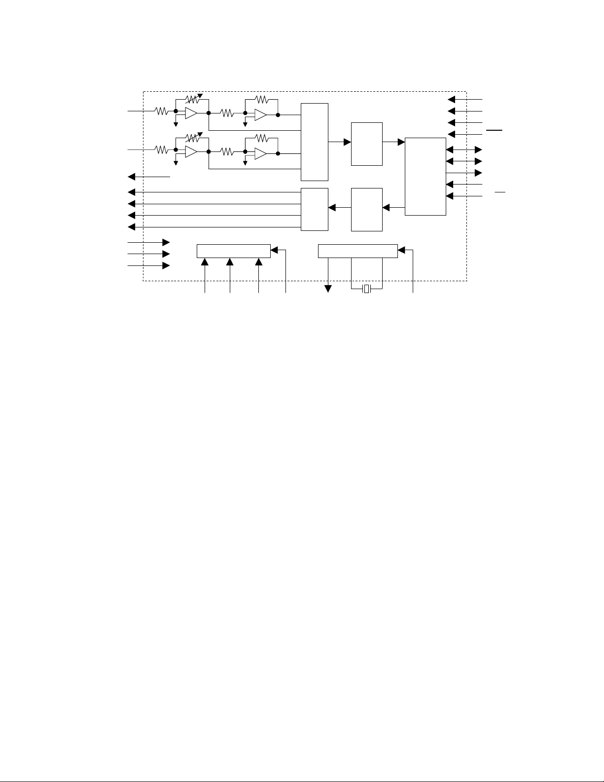
n Block Diagram
VD
AINL
AINR
VCOM
AOUTL+
AOUTLAOUTR+
AOUTR-
VREF
VA
AGND
ADC
DAC
Control Register I/F Clock Gen. & Divider
CS CCLK CDTI CIF CLKO XTO XTI XTALE
HPF
DATT
Audio I/F
Controller
DATT
SMUTE
VT
DGND
PD
LRCK
BICK
SDTO
SDTI
M/ S
Block Diagram
M0050-E-01 1999/5
- 2 -
Page 3

ASAHI KASE I [AK4524]
n Ordering Guide
AK4524VF -10~+70°C 28pin VSOP (0.65mm pitch)
AKD4524 Evaluation Board
n Pin Layout
VCOM
AINR
AINL
VREF
AGND
VA
(Internal pull down) TEST
XTO
XTI
XTALE
LRCK
BICK
SDTO
1
2
3
4
5
6
7
8
9
10
11
12
13
AK4524
Top
View
28
27
26
25
24
23
22
21
20
19
18
17
16
AOUTR+
AOUTR-
AOUTL+
AOUTL-
DGND
VD
VT
CLKO
M/ S
PD
CIF
CS
CCLK
SDTI CDTI
14 15
M0050-E-01 1999/5
- 3 -
Page 4
ASAHI KASE I [AK4524]
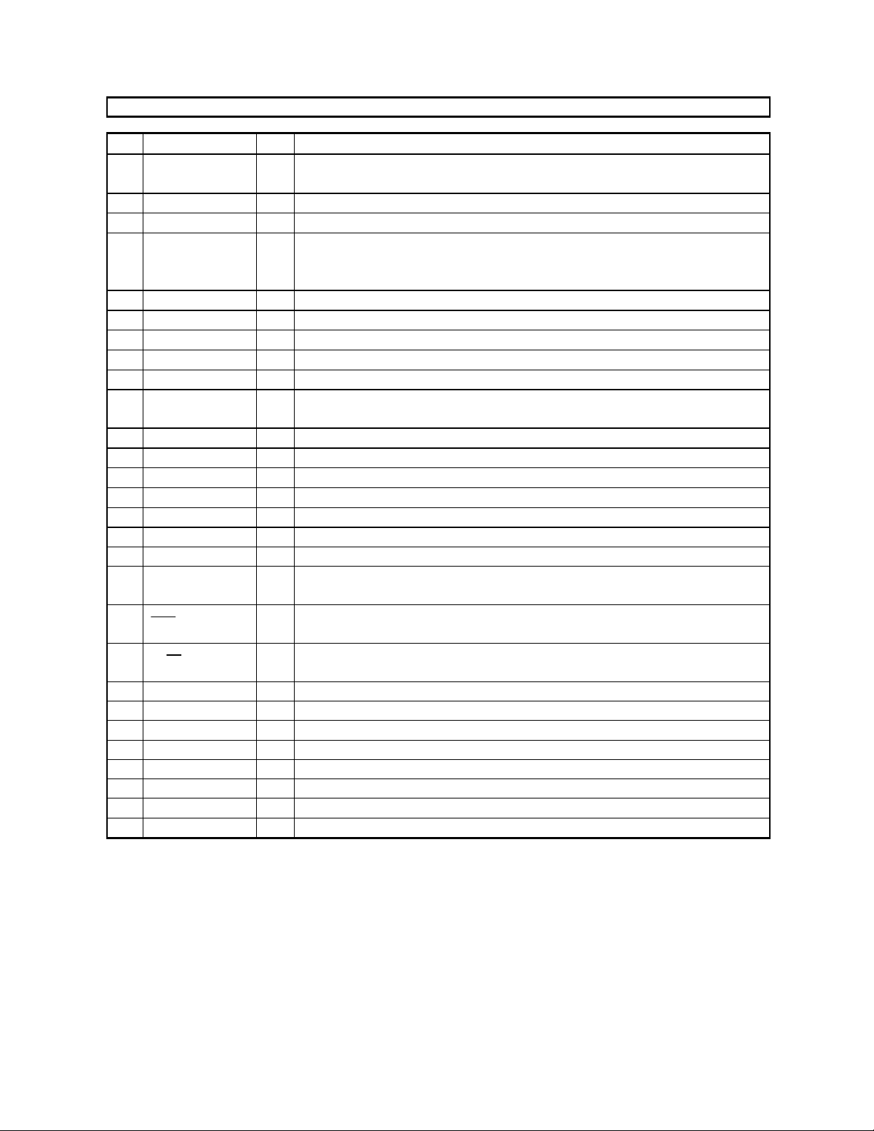
PIN/FUNCTION
No. Pin Name I/O Function
1VCOM O
2 AINR I Rch Analog Input Pin
3 AINL I Lch Analog Input Pin
4VREF I
5 AGND - Analog Ground P i n
6 VA - Analog Power Supply Pin, 4.75 ~ 5.25V
7 TEST I T est Pin (Internal pull-down pin)
8XTO OX’tal Output Pin
9 XTI I X’tal/Master Clock Input Pin
10 XTALE I
11 LRCK I/O Input/Output Channel Clock Pi n
12 BICK I/O Audio Serial Data Clock Pin
13 SDTO O Audio Serial Data Output Pin
14 SDTI I Audio Serial Data Input Pin
15 CDTI I Control Data Input Pin
16 CCLK I Control Data Clock Pin
17 CS I Chip Select Pin
18 CIF I
19 PD I
20 M/ S I
21 CLKO O Master Clock Output Pin
22 VT - Output Buffer Power Supply Pin, 2.7 ~ 5.25V
23 VD - Digital Power Supply Pin, 4.75 ~ 5.25V
24 DGND - Digital Ground Pin
25 AOUTL- O Lch Negative Analog Output Pin
26 AOUTL+ O Lch Positive Analog Output Pin
27 AOUTR- O Rch Negative Analog Output Pin
28 AOUTR+ O Rch Positive Analog Output Pin
Common Voltage Output Pin, VA/2
Bias voltage of ADC inputs and DAC outputs.
Voltage Reference Input Pin, VA
Used as a voltage reference by ADC & DAC. VREF is connected externally to
filtered VA.
X’tal Osc Enable Pin
“H”: Enable, “L”: Disable
Control Data I/F Format Pin
“H”: CS falling trigger, “L”: CS rising trigger
Power-Down M ode Pin
“H”: Power up, “L”: Power down, reset and initialize the control register.
Master/Slave Mode Pin
“H”: Master mode, “L”: Slave mode
Note: All input pins except pull-down pins should not be left floating.
M0050-E-01 1999/5
- 4 -
Page 5
ASAHI KASE I [AK4524]
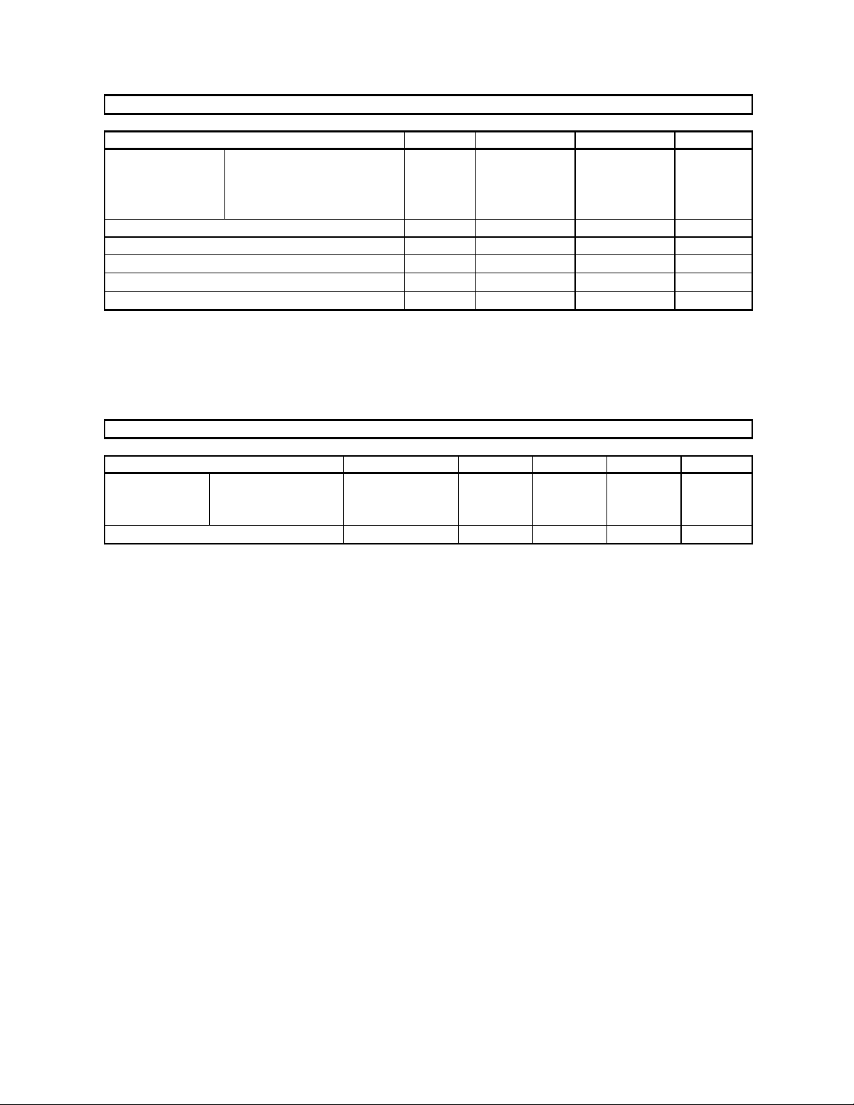
ABSOLUTE MAXI MUM RATINGS
(AGND, DGND=0V; Note 1)
Parameter Symbol min max Units
Power Supplies: Analog
Digital
Output Buffer
VD-VA
Input Current, Any Pin Except Supplies IIN Analog Input Voltage VINA -0.3 VA+0.3 V
Digital Input Voltage VIND -0.3 VA+0.3 V
Ambient Temperature (powered applied) Ta -10 70
Storage Temperature Tstg -65 150
Note:1. All voltages with respect to ground.
WARNING: Operation at or beyond these limits may result in permanent damage to the device.
Normal operation is not guaranteed at these extremes.
VA
VD
VT
VDA
-0.3
-0.3
-0.3
-
6.0
6.0
6.0
0.3
10 mA
±
V
V
V
V
C
°
C
°
RECOMMENDED OPERATING CONDITIONS
(AGND, DGND=0V; Note 1)
Parameter Symbol min typ max Units
Power Supplies
(Note 2)
Voltage Reference VREF 3.0 - VA V
Analog
Digital
Output Buffer
VA
VD
VT
4.75
4.75
2.7
5.0
5.0
3.0
5.25
VA
VD
V
V
V
Note:1. All voltages with respect to ground.
2. VA and VD should be powered at the same time or VA should be powered earlier than VD.
The power up sequence between VA and VT, or VD and VT is not critical.
*AKM assumes no responsibility for the usage beyond the conditions in this datasheet.
M0050-E-01 1999/5
- 5 -
Page 6
ASAHI KASE I [AK4524]
ANALOG CHARA CTERISTICS
(Ta=25°C; VA, VD, VT=5.0V; AGND=DGND=0V; VREF=VA; fs=44.1kHz; Signal Frequency =1kHz; 24bit Data;
Measurement frequency = 10Hz ~ 20kHz at fs=44.1kHz, 10Hz ~ 40kHz at fs=96kHz; unless otherwise specified)
Parameter min typ max Units
Input PGA Characteristics:
Input Voltage (Note 3) 2.7 2.9 3.1 Vpp
Input Resistance 5 10 15 k
Step Size 0.2 0.5 0.8 dB
Gain Control Range 0 18 dB
ADC Analog Input Characteristics: IPGA=0dB
Resolution 24 Bits
S/(N+D) (-0.5dBFS) fs=44.1kHz
fs=96kHz
DR (-60dBFS) fs=44.1kHz, A-weighted
fs=96kHz
S/N fs=44.1kHz, A-weighted
fs=96kHz
Interchannel Isolation 90 105 dB
Interchannel Gain Mismatch 0.2 0.5 dB
Gain Drift 20 - ppm/°C
Power Supply Rejection (Note 4) 50 - dB
DAC Analog Output Characteristics:
Resolution 24 Bits
S/(N+D) (0dBFS) fs=44.1kHz
fs=96kHz
DR (-60dBFS) fs=44.1kHz, A-weighted
fs=96kHz
S/N fs=44.1kHz, A-weighted
fs=96kHz
Interchannel Isolation 100 110 dB
Interchannel Gain Mismatch 0.2 0.5 dB
Gain Drift 20 - ppm/°C
Output Voltage (Note 5) 5.0 5.4 5.8 Vpp
Load Resistance (In case of AC load) 1 k
Output Current (In case of AC load) 1.5 mA
Load Capacitance 25 pF
84
80
94
88
94
88
88
85
104
96
104
96
90
88
100
96
100
96
94
93
110
104
110
104
W
dB
dB
dB
dB
dB
dB
dB
dB
dB
dB
dB
dB
W
Note: 3. Full scale (0dB) of the input voltage at PGA=0dB.
This voltage is proportional to VREF. Vin=0.58 x VREF.
4. PSR is applied to VA, VD, VT with 1kHz, 50mVpp. VREF pin is held a constant voltage.
5. Full scale (0dB) of the output voltage when summing the differential outputs, AOUT+/- by unity gain.
This voltage is proportional to VREF. Vout=1.08 x VREF x Gain.
M0050-E-01 1999/5
- 6 -
Page 7
ASAHI KASE I [AK4524]
Parameter min typ max Units
Power Supplies
Power Supply Current
Normal Operation ( PD
VA
VD+VT (fs=44.1kHz)
(fs=96kHz)
Power-down mode ( PD
VA
VD+VT
Note: 6. XTALE=”L” and all digital input pins are held VD or DGND.
= “H”)
= “L”) (Note 6)
30
16
24
10
10
45
24
36
100
100
mA
mA
mA
uA
uA
FILTER CHARACTERISTICS
(Ta=25°C; VA, VD=4.75 ~ 5.25V; VT=2.7 ~ 5.25V; fs=44.1kHz; DEM=OFF)
Parameter Symbol min typ max Units
ADC Digital Filter (Decimation LPF):
Passband (Note 7) -0.005dB
-0.02dB
-0.06dB
-6.0dB
Stopband SB 24.34 kHz
Passband Ripple PR
Stopband Attenuation SA 80 dB
Group Delay (Note 8) GD 31 1/fs
Group Delay Distortion
ADC Digital Filter (HPF):
Frequency Respons e (Note 5) -3dB
-0.5dB
-0.1dB
DAC Digital Filter:
Passband (Note 7) -0.01dB
-6.0dB
Stopband SB 24.1 kHz
Passband Ripple PR
Stopband Attenuation SA 75 dB
Group Delay (Note 8) GD 30 1/fs
DAC Digital Filter + SCF:
Frequency Response:
0 ~ 20.0kHz
~ 40kHz (Note 9)
PB 0
-
-
-
GD 0 us
D
FR 0.9
PB 0
- 22.05
FR
20.02
22.20
22.05
2.7
6.0
0.2
±
0.3
±
19.76
-
-
-
0.005 dB
±
20.0
-
0.005 dB
±
kHz
kHz
kHz
kHz
Hz
Hz
Hz
kHz
kHz
dB
dB
Note: 7. The passband and stopband frequencies scale with fs. For example, 20.02kHz at -0.02dB is 0.454 x fs.
The reference frequency of these responses is 1kHz.
8. The calculating delay time which occurred by digital filtering. This time is from the input of analog signal to
setting the 24bit data of both channels to the output register for ADC.
For DAC, this time is from setting the 24bit data of both channels on input register to the output of analog
signal.
9. fs=96kHz.
M0050-E-01 1999/5
- 7 -
Page 8
ASAHI KASE I [AK4524]
DIGITAL CHARACTERISTICS
(Ta=25°C; VA, VD=4.75 ~ 5.25V; VT=2.7 ~ 5.25V)
Parameter Symbol min typ Max Units
High-Level Input Voltage
Low-Level Input Voltage
High-Level Output Voltage (Iout=-100uA) (Note 10)
Low-Level Output Voltage (Iout=100uA)
Input Leakage Current Iin - -
VIH
VIL
VOH
VOL
2.2
-
2.7 / VT-0.5
-
-
-
-
-
-
0.8
-
0.5
10 uA
±
V
V
V
V
Note: 10. Min value is lower voltage of 2.7V or VT-0.4V.
SWITCHING CHARACTERISTICS
(Ta=25°C; VA, VD=4.75 ~ 5.25V, VT=2.7 ~ 5.25V; CL=20pF)
Parameter Symbol min typ max Units
Master Clock Timing
Crystal Resonator Frequency 11.2896 24.576 MHz
External Clock Frequency
CLKO Output
(X’tal mode)
Pulse Width Low
Pulse Width High
Frequency
Duty Cycle
fCLK
tCLKL
tCLKH
fMCK
dMCK
8.192
0.4/fCLK
0.4/fCLK
11.2896
35
49.152 MHz
ns
ns
24.576
65
MHz
%
LRCK Frequency
Normal Speed Mode (DFS0=”0”, DFS1=”0”)
Double Speed Mode (DFS0=”1”, DFS1=”0”)
Quad Speed Mode (DFS0=”0”, DFS1=”1”)
Duty Cycle Slave mode
Master mode
fsn
fsd
fsq
32
64
128
45
48
96
192
55 %
50
kHz
kHz
kHz
%
Audio Interface Timing
Slave mode
BICK Period
BICK Pulse Width Low
Pulse Width High
LRCK Edge to BICK “” (Note 11)
BICK “” to LRCK Edge (Note 11)
2
LRCK to SDTO (MSB) (Except I
S mode)
BICK “¯” to SDTO
SDTI Hold Time
SDTI Setup Time
tBCK
tBCKL
tBCKH
tLRB
tBLR
tLRS
tBSD
tSDH
tSDS
81
33
33
20
20
40
40
20
20
ns
ns
ns
ns
ns
ns
ns
ns
ns
Master mode
BICK Frequency
BICK Duty
BICK “¯” to LRCK
BICK “¯” to SDTO
SDTI Hold Time
SDTI Setup Time
fBCK
dBCK
tMBLR
tBSD
tSDH
tSDS
-20
-20
20
20
64fs
50
20
20
Hz
%
ns
ns
ns
ns
Note 11. BICK rising edge must not occur at the same time as LRCK edge.
M0050-E-01 1999/5
- 8 -
Page 9
ASAHI KASE I [AK4524]
Parameter Symbol min typ max Units
Control Interface Timing
CIF=”0”
CCLK Period
CCLK Pulse Width Low
Pulse Width High
CDTI Setup Time
CDTI Hold Time
CS “H” Time
CS “L” Time
CS “” to CCLK “”
CCLK “” to CS “”
tCCK
tCCKL
tCCKH
tCDS
tCDH
tCSW
tCSW
tCSS
tCSH
200
80
80
40
40
150
150
150
50
ns
ns
ns
ns
ns
ns
ns
ns
ns
CIF=”1”
CCLK Period
CCLK Pulse Width Low
Pulse Width High
CDTI Setup Time
CDTI Hold Time
CS “H” Time
CS “L” Time
CS “¯” to CCLK “”
CCLK “” to CS “¯”
tCCK
tCCKL
tCCKH
tCDS
tCDH
tCSW
tCSW
tCSS
tCSH
200
80
80
40
40
150
150
150
50
ns
ns
ns
ns
ns
ns
ns
ns
ns
Reset Timing
PD
Pulse Width (Note 12)
RSTAD “” to SDTO valid (Note 13)
tPD
tPDV
150
516
ns
1/fs
Note:12. The AK4524 can be reset by bringing PD “L”.
13. These cycles are the number of LRCK rising from RSTAD bit.
M0050-E-01 1999/5
- 9 -
Page 10
ASAHI KASE I [AK4524]
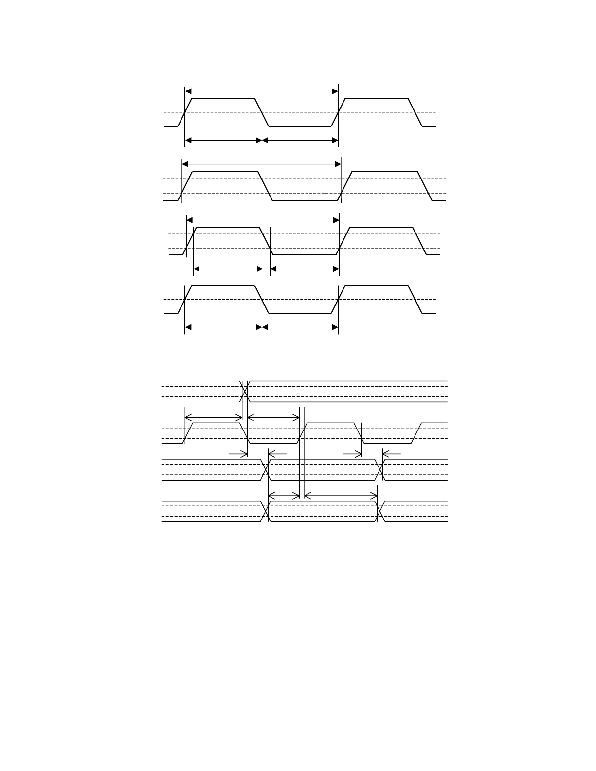
n Timing Diagram
1/fCLK
MCLK
LRCK
BICK
CLKO
LRCK
tCLKH
1/fs
tBCK
tBCKH
tH
dMCK=tH/(tH+tL) or tL/(tH+tL)
Clock Timing
tBLR tLRB
1.5V
tCLKL
VIH
VIL
VIH
VIL
tBCKL
1.5V
tL
VIH
VIL
BICK
SDTO
SDTI
tLRS tBSD
tSDS
Audio Interface Timing (Slave mode)
tSDH
VIH
VIL
VIH
VIL
VIH
VIL
M0050-E-01 1999/5
- 10 -
Page 11

ASAHI KASE I [AK4524]
LRCK
BICK
SDTO
SDTI
CS(CIF=H)
CS(CIF=L)
CCLK
CDTI
tMBLR
tSDS
Audio Interface Timing (Master mode)
tCSS
C1 C0 R/W A4
tCCKL tCCKH
tCDS tCDH
VIH
VIL
VIH
VIL
tBSD
VIH
VIL
tSDH
VIH
VIL
VIH
VIL
VIH
VIL
VIH
VIL
VIH
VIL
CS(CIF=H)
CS(CIF=L)
CCLK
CDTI
WRITE Command Input Timing
D3 D2 D1 D0
WRITE Data Input Timing
tPD
PD
Power Down & Reset Timi ng
tCSW
VIH
VIL
VIH
VIL
tCSH
VIH
VIL
VIH
VIL
VIL
M0050-E-01 1999/5
- 11 -
Page 12

ASAHI KASE I [AK4524]
OPERATION OVERVI EW
n System Clock Input
The master clock (MCLK) can be either a crystal res onator placed across the XTI and XTO pin, or external clock in put to
the XTI pin with the XTO pin left f loating. The mas ter clock frequen cy can be selected by CMODE an d CKS0-1 (Table 1).
The sampling speed (normal speed mode, double speed mode or four times speed monitor mode) is selected by DFS0-1
(Table 2). The ADC is powered down during four times speed monitor mode. The frequency of the master clock output
(CLKO) is the same as MCLK frequency and the output can be enabled or disabled by XTALE pin. When the CLKO
output is not used externally, it should be disabled.
When using a crystal oscillator, external loading capacitors (between XTI/XTO and DGND) are required.
In slave mode, the LRC K clock in put m u st be s y nchron ized w ith MCL K, how ev er th e phase is not critical. Intern al tim in g
is synchronized to LRCK upon power-up. All external clocks must be present unless PD
down by control register, otherwise excessive current may result from abnormal operation of internal dynamic logic. In
master mode, the clocks should be supplied by critical oscillation except for power down or the external clock (MCLK)
should not be stopped.
=”L” or all parts are powered
CMODE CKS1 CKS0 MCLK
0 0 0 256fsn
0 0 1 512fsn
0 1 0 1024fsn
1 0 0 384fsn
1 0 1 768fsn
Table 1. Master clock frequency select
* fsn is a sampling rate at normal speed mode.
DFS1 DFS0 Sampling Rate Monitor mode
0 0 fsn Normal speed 0 1 fsd=2 x fsn Double speed 1 0 fsq=4 x fsn 4 times speed (SDTO=”L”) Simple Decimation
1 1 fsq=4 x fsn 4 times speed (SDT O=”L”) 2 tap filter
Table 2. Sampling speed
MCLK
256fsn 11.2896MHz 12.288MHz 256fsn N/A N/A
512fsn 22.5792MHz 24.576MHz 512fsn 256fsd 128fsq
1024fsn 45.1584MHz 49.152MHz 1024fsn 512fsd 256fsq
384fsn 16.9344MHz 18.432MHz 384fsn N/A N/A
768fsn 33.8688MHz 36.864MHz 768fsn 384fsd 192fsq
fsn=44.1kHz fsn=48kHz
Normal Doub le 4 times
at reset
at reset
Table 3. Master clock frequency
* X’tal mode operates from 11.2896MHz to 24.576MHz.
* The frequency over 24.576MHz supports only external clock mode.
M0050-E-01 1999/5
- 12 -
Page 13

ASAHI KASE I [AK4524]
)
)
(o)
(o)
n Audio Serial Interface Format
Five serial modes selected by the DIF0 and DIF1 pins are supported as shown in Table 4. In all modes the serial data has
MSB first, 2’s compliment format. The SDTO is clocked out on the falling ed ge of BICK and the SDTI is latched on the
rising edge. The interface supports both master mode and slave mode. In master mode, BICK and LRCK are outputs and
the frequency of BICK is fixed to 64fs.
Mode DIF2 DIF1 DIF0 SDTO SDTI LRCK BICK
0 0 0 0 24bit, MSB justified 16bit, LSB justified H/L
1 0 0 1 24bit, MSB justified 20bit, LSB justified H/L
2 0 1 0 24bit, MSB justified 24bit, MSB justified H/L
3 0 1 1 24bit, IIS (I2S) 24bit, IIS (I2S) L/H
4 1 0 0 24bit, MSB justified 24bit, LSB justified H/L
32fs
³
40fs
³
48fs
³
48fs
³
48fs
³
at reset
Table 4. Audio data format
LRCK
0 1 2 9 10 12 13 15 0 1 2 9 10 12 13 15 0231
31114
1411
BICK(32fs)
SDTO
SDTI(i)
BICK(64fs
SDTO(o)
SDTI(i
LRCK
BICK(64fs)
SDTO
SDTI(i)
22 12 23 22 1215 14 23
15 14 13
012 1917 18 20 31 0 1 2 1917 18 20 31 0231
22 4 23 22 7 6 4 23
Don’t Care Don’t Care
SDTO-19:MSB, 0:LSB; SDTI-15:MSB, 0:LSB
15 14
33
21 5 3
13
57
76
1315
Lch Data Rch Data
9811 1021
16043 115 054
2
30
114 012 11 114 012 11
21
14 13 7 6 3 2 15
21
15 13 22
89101113
3
5
Figure 1. Mode 0 Timing
0 1 2 12 13 14 24 25 31 0 1 2 12 13 14 24 25 31 0231
22 0 23 22 12 11 10 0 23
Don’t Care Don’t Care
SDTO-23:MSB, 0:LSB; SDTI-19:MSB, 0:LSB
12 11 10
118 019 8 7 118 019 8 7
Lch Data Rch Data
Figure 2. Mode 1 Timing
M0050-E-01 1999/5
- 13 -
Page 14

ASAHI KASE I [AK4524]
(o)
(o)
(o)
LRCK
0 1 2 18 19 20 21 22 0 1 2 18 19 20 2221 0 1
23 24 25 23 24 25
BICK(64fs)
SDTO
SDTI(i)
LRCK
BICK(64fs)
SDTO
SDTI(i)
LRCK
BICK(64fs)
SDTO
23 22 4 23 22 5454
23:MSB, 0:LSB
5
54
122 023 3 2 122 023 3 2
Don’t Care Don’t Care
Lch Data Rch Data
10321032 23
Figure 3. Mode 2 Timing
0 1 2 3 19 20 21 22 0 1 2 3 19 20 2221 0 1
23 22 4 23 22 5454
23:MSB, 0:LSB
5
54
Lch Data Rch Data
23 24 25 23 24 25
10321032
122 023 3 2 122 023 3 2
Don’t Care Don’t Care
Figure 4. Mode 3 Timing
0 1 2 8 9 10 20 21 31 0 1 2 8 9 10 20 21 31 0231
22 0 23 22 16 15 14 0 23
16 15 14
SDTI(i)
Don’t Care Don’t Care
23:MSB, 0:LSB
Lch Data Rch Data
122 023 12 11 122 023 12 11
Figure 5. Mode 4 Timing
M0050-E-01 1999/5
- 14 -
Page 15

ASAHI KASE I [AK4524]
n Input Volume
The AK4524 includes two channel independent analog volumes (IPGA) with 37 levels, 0.5dB step in front of ADC and
digital volumes (IATT) with 128 levels (includin g MUTE) after ADC. The control data of both volum es are assigned in the
same register address. When MSB of the register is “1”, the IPGA changes and the IATT changes at MSB “0”.
The IPGA is analog volumes and im proves S/N com pared with digital volum e (Table 5). Level ch ang es only occu r du ring
zero-crossings to minimize switching noise. Zero-crossing detection is performed channel independently. If there is no
zero-crossings, then the level will change after a time-out. The time-out period (To) scales with fs. The periods of 256/fs,
512/fs, 1024/fs and 2048/fs are selectable by ZTM1-0 bits in normal speed mode. If new value is written to the IPGA
register before IPGA changes by zero-crossing or time-out, the previous value becomes invalid. And then the timer
(channel independent) for time-out is reset and the timer restarts for new IPGA value. Zero-crossing detection can be
enabled by ZCEI in the control register.
The IATT is a pseudo-log volume linear-interpolated internally. When changing the level, the transition between ATT
values has 8032 levels and is done by soft changes. Therefore, there is not any switching noise.
Input Gain Setting
0dB +6dB +18dB
fs=44.1kHz, A-weight 100dB 98dB 90dB
Table 5. IPGA+ADC S/N
ZTM1 ZTM0 fsn fsd
0 0 256 512
0 1 512 1024
1 0 1024 2048
1 1 2048 4096
Table 6. LRCK cycles for timeout period
at reset
n Digital High Pass Filter
The ADC has a digital high pass filter for DC offset cancel. The cut-off frequency of the HPF is 0.9Hz at fs=44.1kHz and
also scales with sampling rate (fs).
n Output Volume
The Ak4524 includes digital volumes (OATT) with 128 levels (including MUTE) which have the same architecture as
IATT’s in front of DAC. T he OATT is a pseudo-log volume linear-interpolated internally. When changing the level, the
transition between ATT values has 8032 levels and is done by soft changes. Therefore, there is not any switching noise.
M0050-E-01 1999/5
- 15 -
Page 16

ASAHI KASE I [AK4524]
n De-emphasis Filter
The DAC includes the digital de-emphasis filter (tc=50/15us) by IIR filter. This filter corresponds to three frequencies
(32kHz, 44.1kHz, 48kHz). This setting is done via contorl register. This filter is always OFF at double speed and four times
speed modes.
No DEM1 DEM0 Mode
0 0 0 44.1kHz
10 1 OFF
at reset
2 1 0 48kHz
3 1 1 32kHz
Table 7. De-emphasis control (DFS0=DFS1=”0”)
n Soft Mute Operation
Soft mute operation is performed at digital domain. When SMUTE goes “H”, the output signal is attenuated by -¥ during
1024 LRCK cycles. When SMUTE is returned to “L”, the m u te is can celled and th e ou tpu t attenuation g radu ally changes
to 0dB during 1024 LRCK cycles. If the soft mute is cancelled within 1024 LRCK cycles after starting the operation, the
attenuation is discontinu ed and retu rned to 0dB. The sof t m ute is eff ective for ch angin g the si gnal source without stopping
the signal transmission.
Soft mute function is independent to output volume and cascade connected between both functions.
SMUTE
Attenuation
0dB
-
¥
1024/fs
(1)
GD
(2)
1024/fs
GD
Figure 6. Soft Mute
Notes:
(1) The output signal is attenuated by -¥ during 1024 LRCK cycles (1024/fs).
(2) Analog output corresponding to digital input has the group delay (GD).
(3) If the soft mute is cancelled within 1024 LRCK cycles, the attenuation is discontinued and returned to 0dB.
(3)
M0050-E-01 1999/5
- 16 -
Page 17

ASAHI KASE I [AK4524]
n Power Down & Reset
The ADC and DAC of AK4524 are placed in the power-down mode by bringing a power down pin, PD “L” and each
digital filter is also reset at the same time. The internal register values are initialized by PD
“L”. This reset should always
be done after power-up. And then as both control reg is ters of ADC and DAC g o reset s t ate (RSTAD =RSTDA =”0”), each
register sholud be cancelled after doing the needed setting. In case of the ADC, an analog initialization cycle starts after
exiting the power-down or reset state. Therefore, the output data, SDTO becomes available after 516 cycles of LRCK
clock. This initialization cycle does not affect the DAC operation. Power down mode can be also controlled by the registers
(PWAD, PWDA).
Power Supply
PD pin
RSTAD(register)
RSTDA(register)
PWAD(register)
PWDA(register)
PWVR(register)
ADC Internal State
IATT
SDTO
DAC Internal State
OATT
AOUT
External Mute
Example
External clocks
in slave mode
INITA: Initializing period of ADC analog section (516/fs).
·
PD: Power down state. The contents of all registers are hold.
·
XXH: The current value in ATT register.
·
FI: Fade in. After exiting power down and reset state, ATT value fades in.
·
AOUT: Some pop noise may occur at “*”.
·
PD Reset INITA Normal PD INITA Normal
00H 00H ® XXH XXH 00H 00H ® XXH XXH
“0” “0”FI Output FI Output
PD Reset PDNormal Normal
00H 00H ® XXH XXH 00H 00H ® XXH XXH
“0” “0”FI Output FI
MCLK, LRCK, BICK
The clocks can be stopped.
Figure 7. Reset & Power down sequence
****
M0050-E-01 1999/5
- 17 -
Page 18

ASAHI KASE I [AK4524]
n Relationship between Clock Operation and Power-Down
XTALE pin controls the clock outputs. The operation in slave mode is shown Table 8. Table 9 shows the master mode
operation. When a crystal oscillator is used, XTALE pin is set to “H”. XTALE pin should be “L” at external clock mode.
Slave Mode
XTAL mode Inhibit Inhibit Normal operation
EXT Clock mode Normal operation
Master Mode
XTAL mode Inhibit Inhibit Normal operation
EXT Clock mode Normal operation
PD
XTI = MCLK in
XTO = L
CLKO = L
LRCK = Input
BICK = Input
Table 8. Clock operation at slave mode (M/ S = L)
PD
XTI = MCLK in
XTO = L
CLKO = L
LRCK = Output
BICK = Output
XTALE=L XTALE=H
=H PD =L PD =H PD =L
XTAL = Oscillation
CLKO = Output
LRCK = Input
BICK = Input
Shut off
XTI = MCLK in
XTO = L
CLKO = L
LRCK = Input
BICK = Input
XTALE=L XTALE=H
=H PD =L PD =H PD =L
Shut off
XTI = MCLK in
XTO = L
CLKO = L
LRCK = H
BICK = L
Inhibit Inhibit
XTAL = Oscillation
CLKO = Output
LRCK = Output
BICK = Output
Inhibit Inhibit
Power down
XTAL = Oscillation
CLKO = Output
LRCK = Input
BICK = Input
Power down
XTAL = Oscillation
CLKO = Output
LRCK = H
BICK = L
Table 9. Clock operation at master mode (M/ S = H)
M0050-E-01 1999/5
- 18 -
Page 19

ASAHI KASE I [AK4524]
n Serial Control Interface
The internal registers are written by the 3 wire uP interface pins: CS, CCLK, CDTI. The data on this interface consists of
Chip address (2bits, C0/1) Read/Write (1b it), Register address (MSB first, 5bits) and Control data (MSB first, 8bits).
Address and data is clocked in on the rising edge of CCLK. Data is latched after the 16th rising edge of CCLK, after a
high-to-low transition of CS. The operation of the control serial port may be completely asynchronous with the audio
sample rate. The maxim um clock speed of th e CCLK is 5MHz. The CS shou ld be “H” or “ L” if n o access. The chip address
is fixed to “10”. Writing is invalid for the access to th e chip address except for “10”. PD
= “L” resets the registers to their
default values.
CS (CIF=1)
CS (CIF=0)
67891011
12 13 14 15
CCLK
CDTI
012345
C1 C0 A 2A3 A1 A0A4 D7 D6 D5 D4 D3 D2 D1 D0R/W
C1-C0: Chip Address (Fixed to “10”)
R/W: READ/WRITE (Fixed to “1”:WRIT E)
A4-A0: Register Address
D7-D0: Control data
Figure 8. Control I/F Timing
* READ command is not supported.
n Register Map
Addr Register Name D7 D6 D5 D4 D3 D2 D1 D0
00HPower Down Control 00000PWVRPWADPEDA
01HReset Control 000000RSTADRSTDA
02H Clock and Format Control DIF2 DIF1 DIF0 CMODE CKS1 CKS0 DFS1 DFS0
03H Deem and Volume Control SMUTE 0 0 ZCEI ZTM1 ZTM0 DEM1 DEM0
04H Lch IPGA Control IPGL7 IPGL6 IPGL5 IPGL4 IPGL3 IPGL2 IPGL1 IP GL0
05H Rch IPGA Control IPGR7 IPGR6 IPGR5 IPGR4 IPGR3 IPGR2 IPGR1 IPGR0
06H Lc h ATT Control 0 ATTL6 ATTL5 ATTL4 ATTL3 ATTL2 ATTL1 ATTL0
07H R ch ATT Control 0 ATTR6 ATTR5 ATTR4 ATTR3 ATTR2 ATTR1 ATTR0
Note: For addresses from 08H to 1FH, data is not written.
PD
= “L” resets the registers to their default values.
M0050-E-01 1999/5
- 19 -
Page 20

ASAHI KASE I [AK4524]
n
n Control Register Setup Sequence
nn
When PD pin goes “L” to “H” upon power-up etc., the AK4524 should operate by the next sequence. In this case, all
control registers are set to initial values and the AK4524 is in the reset state.
(1) Set the clock mode and the audio data interface mode.
(2) Cancel the reset state by setting RSTAD or RSTDA to “1”. Refer to Reset Contorl Register (01H).
(3) ADC outputs and DAC outputs should be muted externally until cancelling each reset state. In master mode, there is
a possibility the frequency and duty of LRCK and BICK outputs become an abnormal state.
The clock mode should be chang ed after s etting RSTAD an d RSTDA to “ 0”. A t that tim e, A DC ou tputs and DA C outpu ts
should be muted externally. In master mode, there is a possibility the frequency and duty of LRCK and BICK outputs
become an abnormal state.
n
n Register Definitions
nn
Addr Register Name D7 D6 D5 D4 D3 D2 D1 D0
00HPower Down Control 00000PWVRPWADPWDA
RESET 00000111
PWDA: DAC power down
0: Power down
1: Power up
Only DAC section is pow ered dow n by “ 0” and th en the AOUTs go Hi- Z im m ediately . The OATTs also go
“00H”. But the contents of all register are not initialized and enabled to write to the registers. After exiting
the power down mode, the OA TTs fade in the setting value of th e control register (06H & 07H). The analog
outputs should be muted externally as some pop noise may occur when entering to and exiting from this
mode.
PWAD: ADC power down
0: Power down
1: Power up
Only ADC section is powered down by “0” and then the SDTO goes “L” immediately. The IPGAs also go
“00H”. But the contents of all register are not initialized and enabled to write to the registers. After exiting
the power down mode, the IPGAs fade in the setting value of the control register (04H & 05H). At that time,
ADCs output “0” during first 516 LRCK cycles.
PWVR: Vref power down
0: Power down
1: Power up
All sections are powered down by “0” and then both ADC and DAC do not operate. The contents of all
register are not initialized and enabled to write to the registers. When PWAD and PWDA go “0” and PWVR
goes “1”, only VREF section can be powered up.
M0050-E-01 1999/5
- 20 -
Page 21

ASAHI KASE I [AK4524]
Addr Register Name D7 D6 D5 D4 D3 D2 D1 D0
01HReset Control 000000RSTADRSTDA
RESET 00000000
RSTDA: DAC reset
0: Reset
1: Normal Operation
The internal timing is reset by “0” and then the AOUTs go VCOM voltage immediately. The OATTs also
go “00H”. But the contents of all register are not initialized and enabled to write to the registers. After
exiting the power down mode, the OATTs fade in the setting value of the control register (06H & 07H). The
analog outputs should be muted externally as some pop noise may occur when entering to and exiting from
this mode.
RSTDA: ADC reset
0: Reset
1: Normal Operation
The internal timing is reset by “0” and then SDTO goes “L” immediately. The IPGAs also go “00H”. But
the contents of all register are not initialized and enabled to write to the register. After exiting the power
down mode, the IPGAs fade in the setting value of the control register (04H & 05H). At that time, ADCs
output “0” during first 516 LRCK cycles.
Addr Register Name D7 D6 D5 D4 D3 D2 D1 D0
02H Clock and Format Control DIF2 DIF1 DIF0 CMODE CKS1 CKS0 DFS1 DFS0
RESET 01000000
DFS1-0: Sampling Speed Control (see Table 2)
Initial: Normal speed
CMODE, CKS1-0: Master Clock Frequency Select (see Table 1)
Initial: 256fs
DIF2-0: Audio data interface modes (see Table 4)
000: Mode 0
001: Mode 1
010: Mode 2
011: Mode 3
100: Mode 4
Initial: 24bit MSB justified for both ADC and DAC
M0050-E-01 1999/5
- 21 -
Page 22

ASAHI KASE I [AK4524]
Addr Register Name D7 D6 D5 D4 D3 D2 D1 D0
03H Deem and Volume Control SMUTE 0 0 ZCEI ZTM1 ZTM0 DEM1 DEM0
RESET 00011001
DEM1-0: De-emphasis response (see Table 7)
00: 44.1kHz
01: OFF
10: 48kHz
11: 32kHz
Initial: OFF
ZTM1-0: Zero crossing time out period select (see Table 6)
Initial: 1024fs
ZCEI: ADC IPGA Zero crossing enable
0: Input PGA gain changes occur immediately
1: Input PGA gain changes occur only on zero-crossing or after timeout.
Initial: 1 (Enable)
SMUTE: DAC Input Soft Mute control
0: Normal operation
1: DAC outputs soft-muted
The soft mute is independent of the output ATT and performed digitally.
Addr Register Name D7 D6 D5 D4 D3 D2 D1 D0
04H Lch IPGA Control IPGL7 IPGL6 IPGL5 IPGL4 IPGL3 IPGL2 IPGL1 IP GL0
05H Rch IPGA Control IPGR7 IPGR6 IPGR5 IPGR4 IPGR3 IPGR2 IPGR1 IPGR0
RESET 01111111
IPGL/R7-0: ADC Input Gain Level
Refer to Table 10
Initial: 7FH (0dB)
Digital ATT with 128 levels operates when writing data of less than 7FH. This ATT is a linear ATT with
8032 levels internally and these levels are assigned to pseudo-log data with 128 levels. The transition
between ATT values has 8032 levels and is done by soft changes. For example, when ATT changes from
127 to 126, the internal ATT value decreases from 8031 to 7775 one by one every fs cycles. It takes 8031
cycles (182ms@fs=44.1kHz) from 127 to 0 (Mute).
The IPGAs are set to “00H” when PD
pin goes “L”. After returning to “H”, the IPGAs fade in the initial
value, “7FH” by 8031 cycles.
The IPGAs are set to “00H” when PWAD goes “0”. After returning to “1”, the IPGAs fade in the current
value. But the ADCs output “0” during first 516 cycles.
The IPAGs are set to “00H” when RSTAD goes “0”. After returning to “1”, the IPGAs fade in the current
value. But the ADCs output “0” during first 516 cycles.
M0050-E-01 1999/5
- 22 -
Page 23

ASAHI KASE I [AK4524]
Data
Internal
(DATT)
Gain (dB) Step width (dB)
255 - 165 - +18 -
164 - +18 163 - +17.5 0.5
162 - +17 0.5
:- : 0.5
130 - +1.0 0.5
129 - +0.5 0.5
128 - 0 0.5
127 8031 0 126 7775 -0.28 0.28
125 7519 -0.57 0.29
:: : :
112 4191 -5.65 0.51
111 3999 -6.06 0.41
110 3871 -6.34 0.28
:: : :
96 2079 -11.74 0.52
95 1983 -12.15 0.41
94 1919 -12.43 0.28
:: : :
79 1023 -17.90 0.53
78 975 -18.32 0.42
77 943 -18.61 0.29
:: : :
64 495 -24.20 0.54
63 471 -24.64 0.43
62 455 -24.94 0.30
:: : :
48 231 -30.82 0.58
47 219 -31.29 0.46
46 211 -31.61 0.32
:: : :
32 99 -38.18 0.67
31 93 -38.73 0.54
30 89 -39.11 0.38
:: : :
16 33 -47.73 0.99
15 30 -48.55 0.83
14 28 -49.15 0.60
:: : :
5 10 -58.10 1.58
4 8 -60.03 1.94
3 6 -62.53 2.50
2 4 -66.05 3.52
1 2 -72.07 6.02
00MUTE
IPGA
Analog volume with 0.5dB step
IATT
External 128 levels are converted to internal
8032 linear levels of DATT. Internal DATT
soft-changes between DATAs.
DATT=2^m x (2 x l + 33) – 33
m: MSB 3-bits of data
l: LSB 4-bits of data
Table 10. IPGA code table
M0050-E-01 1999/5
- 23 -
Page 24

ASAHI KASE I [AK4524]
Addr Register Name D7 D6 D5 D4 D3 D2 D1 D0
06H Lc h OATT Cont rol 0 ATTL6 ATTL5 ATTL4 ATTL3 ATTL2 ATTL1 ATTL0
07H R ch OATT Control 0 ATTR6 ATTR5 ATTR4 ATTR3 ATTR2 ATTR1 ATTR0
RESET 01111111
ATTL/R6-0: DAC ATT Level
Refer to Table 11
Initial: 7FH (0dB)
The AK4524 includes digital ATT with 128 levels equivalent to ADC’s.
The OATTs are set to “00H” when PD
value, “7FH” by 8031 cycles.
The OATTs are set to “00H” when PWDA goes “0”. After returning to “1”, the OATTs fade in the current
value.
The OATTs are set to “00H” when RSTDA goes “0”. Afer returning to “1”, the OATTs fade in the current
Value.
0
-10
-20
-30
-40
-50
-60
ATT(dB)
-70
-80
-90
-100
pin goes “L”. After returning to “H”, the OATTs fade in the initial
2
1.8
ATT (dB)
1.6
1.4
1.2
1
0.8
Step (dB)
Step(dB)
0.6
0.4
0.2
0
127 111 95 79 63 47 31 15
Input Data(Level)
Figure 9. ATT characteristics
M0050-E-01 1999/5
- 24 -
Page 25

ASAHI KASE I [AK4524]
Data
Internal
(DATT)
Gain (dB) Step width (dB)
127 8031 0 126 7775 -0.28 0.28
125 7519 -0.57 0.29
:: : :
112 4191 -5.65 0.51
111 3999 -6.06 0.41
110 3871 -6.34 0.28
:: : :
96 2079 -11.74 0.52
95 1983 -12.15 0.41
94 1919 -12.43 0.28
:: : :
79 1023 -17.90 0.53
78 975 -18.32 0.42
77 943 -18.61 0.29
:: : :
64 495 -24.20 0.54
63 471 -24.64 0.43
62 455 -24.94 0.30
:: : :
48 231 -30.82 0.58
47 219 -31.29 0.46
46 211 -31.61 0.32
:: : :
32 99 -38.18 0.67
31 93 -38.73 0.54
30 89 -39.11 0.38
:: : :
16 33 -47.73 0.99
15 30 -48.55 0.83
14 28 -49.15 0.60
:: : :
5 10 -58.10 1.58
4 8 -60.03 1.94
3 6 -62.53 2.50
2 4 -66.05 3.52
1 2 -72.07 6.02
00MUTE
OATT
External 128 levels are converted to internal
8032 linear levels of DATT. Internal DATT
soft-changes between DATAs.
DATT=2^m x (2 x l + 33) – 33
m: MSB 3-bits of data
l: LSB 4-bits of data
Table 11. OATT code table
M0050-E-01 1999/5
- 25 -
Page 26

ASAHI KASE I [AK4524]
SYSTEM DESIGN
Figure 10 & Figu re 11 show the sy stem con nection diagram . This is an example w hich the AK4524 operates at X’tal m ode.
In case of external clock m ode, please refer to Fig ure 11. An ev aluation board (AKD4524) is available wh ich demon strates
application circuits, the optimum layout, power supply arrangements and measurement results.
4.75 ~ 5.25V
Analog Supply
+
10u
VD
Audio
Controller
0.1u
C
C
0.1u
10u
+
1
VCOM
2
AINR
3
AINL
4
VREF
5
AGND
6
VA
TEST
7
8
XTO
XTI
9
10
XTALE
11
LRCK
12
BICK
13
SDTO
14 15
SDTI CDTI
AK4524
AOUTR+
AOUTR-
AOUTL+
AOUTL-
DGND
VD
VT
CLKO
M/ S
PD
CIF
CS
CCLK
28
27
26
25
24
23
22
21
20
19
18
17
16
Rch
LPF
Lch
LPF
0.1u0.1u
Mode
Setting
Rch Out
Lch Out
5
2.7 ~ 5.25V
Digital Supply
Notes:
- X’tal Oscillation circuit is specified from 11.2896MHz to 24.576MHz.
- AGND and DGND of AK4524 should be distributed separately from the ground of external controller etc.
- When AOUT+/- drives some capcitive load, some resistor sholud be added in series between AOUT+/- and
capacitive load.
- All input pins except pull-down pin (TEST) should not be left floating.
Figure 10. Typical Connection Diagram (X’tal mode)
X’tal Frequency C
11.2896MHz, 12.288MHz 33pF
16.384MHz, 16.9344MHz, 18.432MHz 15pF
22.5792MHz, 24.576MHz 10pF
Table 12. External capacitance example for X’tal
(Please contact X’tal oscillator manufacturer)
M0050-E-01 1999/5
- 26 -
Page 27

ASAHI KASE I [AK4524]
4.75 ~ 5.25V
Analog Supply
+
10u
Audio
Controller
0.1u
0.1u
10u
+
1
VCOM
2
AINR
3
AINL
4
VREF
5
AGND
6
VA
TEST
7
8
XTO
XTI
9
10
XTALE
11
LRCK
12
BICK
13
SDTO
14 15
SDTI CDTI
AK4524
AOUTR+
AOUTR-
AOUTL+
AOUTL-
DGND
VD
VT
CLKO
M/ S
PD
CIF
CS
CCLK
28
27
26
25
24
23
22
21
20
19
18
17
16
Rch
LPF
Lch
LPF
0.1u0.1u
Mode
Setting
Rch Out
Lch Out
5
2.7 ~ 5.25V
Digital Supply
Figure 11. Typical Connection Diagram (EXT clock mode)
1. Grounding and Power Supply Decoupli ng
The AK4524 requires careful attention to power supply and grounding arrangements. VA and VD are usually supplied
from analog supply in system. Alternatively if VA and VD are supplied separately, the power up sequence is taken care.
VT is a power supply pin to interface with the external ICs and is supplied from digital supply in system. AGND and
DGND of the AK4524 should be connected to analog ground plane. System analog ground and digital ground should be
connected together near to where the supplies are brought onto the printed circuit board. Decoupling capacitors should be
as near to the AK4524 as possible, with the small value ceramic capacitor being the nearest.
2. Voltage Reference
The differential voltage between VREF an d AGND sets th e analog in put/output rang e. VREF pin is normally connected to
VA with a 0.1uF ceramic capacitor. VCOM is a signal ground of this chip. An electrolytic capacitor 10uF parallel with a
0.1uF ceramic capacitor attached to VCOM pin eliminates the effects of high frequency noise. No load current may be
drawn from VCOM pin. All signals, especially clocks, should be kept away from the VREF and VCOM pins in order to
avoid unwanted coupling into the AK4524.
M0050-E-01 1999/5
- 27 -
Page 28

ASAHI KASE I [AK4524]
3. Analog Inputs
The IPGA inputs are single-en ded and the inpu t resistance 5kW (min). The input signal range scales with the VREF voltage
and nominally 0.58 x VREF Vpp centerd in the internal common voltage (about VA/2). Usually the input signal is AC
coupled with capacitor. The cut- off f requency is fc=(1/2pRC). The AK4524 can accept input voltages from AGND to VA.
The ADC output data format is 2’s complem ent. The output code is 7FFFFFH(@24bit) for input above a positive full scale
and 800000H(@24bit) for input below a neg ative f ill scale. The ideal code is 000000H(@24bit) w ith no inpu t sig nal. The
DC offset including ADC own DC offset removed by the internal HPF.
The AK4524 samples the analog inputs at 64fs. The digital filter rejects noise above the stopband except for multiples of
64fs. The AK4524 includes an anti-aliasing filter (RC filter) to attenuate a noise around 64fs.
4. Analog Outputs
The analog outputs are full differential outputs and nominally 0.54 x VREF Vpp centered in the internal common voltage
(about VA/2). The differential outputs are summed externally, Vout=(AOUT+)-(AOUT-) between AOUT+ and AOUT-.
If the summing gain is 1, the output range is 5.4Vpp (typ@VREF=5V). The bias voltage of the external summing circuit is
supplied externally. The input data format is 2’s complement. The output voltage is a positive full scale for
7FFFFFH(@24bit) and a negative full scale for 800000H(@24bit). The ideal AOUT is 0V for 000000H(@24bit).
The internal switched-capacitor filter and the external LPF attenuate the noise generated by the delta-sigma modulator
beyond the audio passband.
Differential outputs can eliminate any DC offset on analog outputs without using capacitors. Figure 12 to Figure 14 show
the example of external op-amp circuit summing the differential outputs.
Vop
1k
1k
4.7k 4.7k
R1
3300p
4.7k
4.7k 470p
R1
When R1=200ohm
fc=93.2kHz, Q=0.712, g=-0.1dB at 40kHz
When R1=180ohm
fc=98.2kHz, Q=0.681, g=-0.2dB at 40kHz
470p
Vop
-
+
Analog
Out
AOUT-
AOUT+
BIAS
47u
0.1u
+
Figure 12. External 2nd order LPF Example (using single supply op-amp)
M0050-E-01 1999/5
- 28 -
Page 29

ASAHI KASE I [AK4524]
AOUT-
AOUT+
4.7k 4.7k
R1
3300p
4.7k
4.7k 470p
R1
When R1=200ohm
fc=93.2kHz, Q=0.712, g=-0.1dB at 40kHz
When R1=180ohm
fc=98.2kHz, Q=0.681, g=-0.2dB at 40kHz
470p
+Vop
-
+
-Vop
Analog
Out
Figure 13. External 2nd order LPF Example (using dual supply op-amp)
180p
AOUT-
AOUT+
4.7k 4.7k
4.7k
+Vop
-
+
Analog
Out
4.7k 180p
-Vop
fc=188kHz
Figure 14. External low cost 1st order LPF Example (using dual supply op-amp)
n Peripheral I/F Example
The digital inputs of the AK4524 are TTL inputs and can accept the s ignal of device w ith a n ominal 3V supply . The digital
output can interface with the peripheral device with a nominal 3V supply when the VT supply operates at a nominal 3V
supply.
5V Analog
DigitalAnalog I/F
AK4524
Audio signal
Control signal
DSP
uP &
Others
3V Digital
3 or 5V Digital
Figure 15. Power supply connection example
M0050-E-01 1999/5
- 29 -
Page 30

ASAHI KASE I [AK4524]
)
PACKAGE
28pin VSOP (Unit: mm
0.675
28
0.22±0.1
1
Seating Plane
*9.8±0.2 1.25±0.2
15
A
0.2
0.10
|
14
0.65
Deta il A
*5.6
±
+0.1
0.15-0.05
0.1±0.1
0.2
±
0.5
1.0
0.2
±
7.6
NOTE: Dimension "*" does not include mold flash.
n
n Package & Lead frame material
nn
Package molding compound: Epoxy
Lead frame material: Cu
Lead frame surface treatment: Solder plate
0-10
°
M0050-E-01 1999/5
- 30 -
Page 31

ASAHI KASE I [AK4524]
MARKING
AKM
AK4524VF
XXXBYYYYC
XXXBYYYYC: data code identifier
XXXB: Lot number (X: Digit number, B: Alpha character)
YYYYC: Assembly date (Y: Digit number, C: Alpha character)
IMPORTANT NOTICE
These products and their specifications are subject to change without notice. Before considering any
·
use or application, consult the Asahi Kasei Micros ystems Co., Ltd. (AKM) s ales off ice or authorized
distributor concerning their current s tatus.
AKM assumes no liability for infringem ent of any patent, intellectual property, or other right in the
·
application or use of any information contained herein.
Any export of these products, or devices or systems containing them, may require an export license or
·
other official approval under the law and regulations of the country of export pertaining to customs and
tariffs, currency exchange, or str ategic m aterials.
AKM products are neither intended nor authorized for use as c ritical com ponents in any safety, life
·
support, or other hazard related device or system, and AKM assumes no responsibility relating to any
such use, except with the express written consent of the Representative Direc tor of AKM. As us ed
here:
(a) A hazard related device or system is one designed or intended f or lif e suppor t or m aintenanc e of
safety or for applications in medicine, aer ospace, nuclear ener gy, or other fields, in which its
failure to function or perform m ay reasonably be expected to result in loss of lif e or in signific ant
injury or damage to person or property.
(b) A critical component is one whose failure to func tion or perfor m m ay reasonably be expected to
result, whether directly or indirectly, in the loss of the safety or effectiveness of the device or
system containing it, and which must theref ore meet ver y high standards of perform ance and
reliability.
It is the responsibility of the buyer or distributor of an AKM product who distributes, dispos es of, or
·
otherwise places the product with a third party to notify that party in advance of the above content and
conditions, and the buyer or distributor agrees to assume any and all responsibility and liability for and
hold AKM harmless from any and all claims arising from the use of said product in the absence of such
notification.
M0050-E-01 1999/5
- 31 -
 Loading...