


Audio
DIF1
8X
De-emphasis
Control
Clock
DFS1
DFS0
8X
DIF0
∆Σ
DAC
AK4386
查询AK4386供应商
ASAHI KASEI [AK4386]
The AK4386 is a 24bit low voltage & low power stereo DAC. The AK4386 uses the Advanced Multi-Bit ∆Σ
architecture, this architecture achieves DR=100dB at 3V operation. The AK4386 integrates a
combination of SCF and CTF filters increasing performance for systems with excessive clock jitter. The
AK4386 is suitable for the portable audio system like MP3 and the home audio systems like STB and TV,
etc as low power and small package. The AK4386 is offered in a space saving 16pin TSSOP package.
100dB 96kHz 24-Bit 2ch
GENERAL DESCRIPTION
FEATURES
o Sampling Rate: 8kHz ∼ 96kHz
o 24-Bit 8 times FIR Digital Filter
o SCF with high tolerance to clock jitter
o Single-ended output buffer
o Digital de-emphasis for 44.1kHz sampling
o I/F Format: 24-Bit MSB justified, 16/24-Bit LSB justified, I2S Compatible
o Master Clock:
512/768/1024/1536fs for Half Speed (8kHz
256/384/512/768fs for Normal Speed (8kHz ∼ 48kHz)
128/192/256/384fs for Double Speed (48kHz ∼ 96kHz)
o CMOS Input Level
o THD+N: −86dB
o DR, S/N: 100dB(@VDD=3.0V)
o Power Supply: 2.2 to 3.6V
o Ta = −40 ∼ 85°C
o 16pin TSSOP
PDN
DEM TEST
MCLK
Divider
∼ 24kHz)
VDD
VSS
VCOM
LRCK
BICK
SDTI
Data
Interface
Interpolator
Interpolator
∆Σ
Modulator
∆Σ
Modulator
SCF
CTF
SCF
CTF
LOUT
ROUT
MS0280-E-00 2003/12
- 1 -
ASAHI KASEI [AK4386]
n Ordering Guide
AK4386VT −40 ∼ +85°C 16pin TSSOP (0.65mm pitch)
AKD4386 Evaluation Board for AK4386
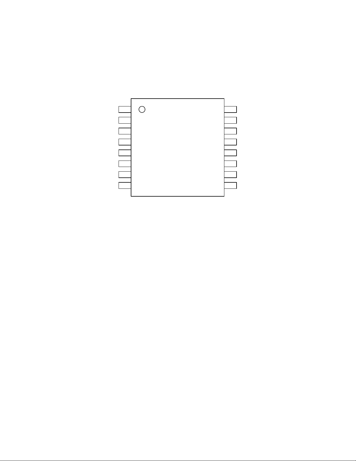
n Pin Layout
MCLK
BICK
SDTI
LRCK
PDN
DFS0
DFS1
DEM
1
2
3
4
Top View
5
6
7
8
16
15
14
13
12
11
10
9
TEST
DIF1
VDD
VSS
VCOM
LOUT
ROUT
DIF0
MS0280-E-00 2003/12
- 2 -
ASAHI KASEI [AK4386]
PIN/FUNCTION
No. Pin Name I/O Function
1 MCLK I Master Clock Input Pin
2 BICK I Audio Serial Data Clock Pin
3 SDTI I Audio Serial Data Input Pin
4 LRCK I Input Channel Clock Pin
5 PDN I
6 DFS0 I Sampling Speed Select 0 Pin
7 DFS1 I Sampling Speed Select 1 Pin
8 DEM I
9 DIF0 I Audio Interface Format 0 Pin
10 ROUT O Rch Analog Output Pin
11 LOUT O Lch Analog Output Pin
12 VCOM O
13 VSS - Ground Pin
14 VDD 15 DIF1 I Audio Interface Format 1 Pin
16 TEST I
Note: All digital input pins should not be left floating.
Full Power Down Mode Pin
“L” : Power down, “H” : Power up
De-emphasis Filter Enable Pin
“L” : OFF, “H” : ON (De-emphasis of fs=44.1kHz is enable.)
Common Voltage Output Pin, 0.55 × VDD
Normally connected to VSS with a 4.7µF (min. 1µF, max. 10µF) electrolytic
capacitor.
Power Supply Pin, 2.2 ∼ 3.6V
TEST Pin
This pin should be connected to VDD.
n Handling of Unused Pin
The unused output pins should be processed appropriately as below.
Classification Pin Name Setting
Analog LOUT, ROUT This pin should be open.
MS0280-E-00 2003/12
- 3 -
ASAHI KASEI [AK4386]
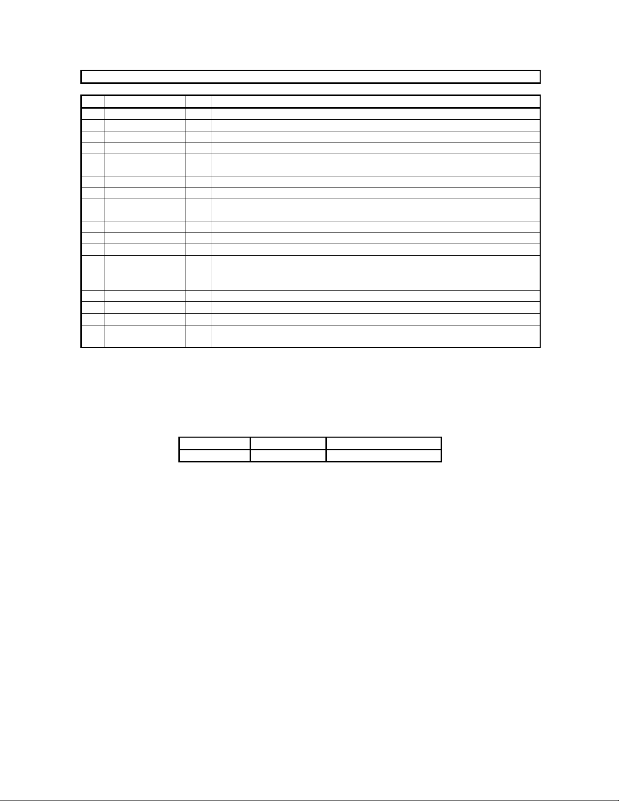
ABSOLUTE MAXIMUM RATINGS
(VSS=0V; Note 1)
Parameter Symbol min max Units
Power Supply VDD
Input Current, Any Pin Except Supplies IIN Digital Input Voltage VIND −0.3 VDD+0.3 V
Ambient Temperature (Powered applied) Ta −40 85 °C
Storage Temperature Tstg −65 150 °C
Note 1. All voltages with respect to ground.
WARNING: Operation at or beyond these limits may result in permanent damage to the device.
Normal operation is not guaranteed at these extremes.
−
0.3 4.6 V
±
10 mA
RECOMMENDED OPERATING CONDITIONS
(VSS=0V; Note 1)
Parameter Symbol min typ max Units
Power Supply VDD 2.2 3.0 3.6 V
Note 1. All voltages with respect to ground.
WARNING: AKM assumes no responsibility for the usage beyond the conditions in this datasheet.
MS0280-E-00 2003/12
- 4 -

ASAHI KASEI [AK4386]
ANALOG CHARACTERISTICS
(Ta=25°C; VDD=3.0V; VSS=0V; fs=44.1kHz, 96kHz; BICK=64fs; Signal Frequency=1kHz; 24bit Data;
Measurement frequency=20Hz ∼ 20kHz at fs=44.1kHz, 20Hz ∼ 40kHz at fs=96kHz; unless otherwise specified)
Parameter min typ max Units
Dynamic Characteristics:
Resolution 24 Bits
THD+N
DR (−60dBFS with A-weighted) 92 100 dB
S/N (A-weighted) 92 100 dB
Interchannel Isolation 80 100 dB
DC Accuracy:
Interchannel Gain Mismatch 0.2 0.5 dB
Gain Drift 100 - ppm/°C
Output Voltage (Note 2) 1.85 2.0 2.15 Vpp
Load Resistance (Note 3) 10 kΩ
Load Capacitance 25 pF
Power Supplies
Power Supply Current
Normal Operation (PDN pin = “H”, fs=44.1kHz)
Normal Operation (PDN pin = “H”, fs=96kHz)
Power Save mode (PDN pin = “H”, MCLK Stop)
Full Power-down mode (PDN pin = “L”) (Note 4)
Note 2. Full-scale voltage (0dB). Output voltage scales with the voltage of VDD, Vout = 0.67 × VDD (typ).
Note 3. For AC-load.
Note 4. All digital input pins are fixed to VDD or VSS.
fs=44.1kHz
BW=20kHz
fs=96kHz
BW=40kHz
0dBFS
−
60dBFS
0dBFS
−60dBFS
−86
−37
−84
−34
6
6.5
1.5
10
−76
-
-
-
9
10
2.5
50
dB
dB
dB
dB
mA
mA
mA
µ
A
MS0280-E-00 2003/12
- 5 -

ASAHI KASEI [AK4386]
FILTER CHARACTERISTICS
(Ta=25°C; VDD=2.2 ∼ 3.6V; fs=44.1kHz; DEM=OFF)
Parameter Symbol min typ max Units
DAC Digital Filter:
Passband (Note 5)
Stopband (Note 5) SB 24.1 kHz
Passband Ripple PR ±0.01 dB
Stopband Attenuation SA 64 dB
Group Delay (Note 6) GD - 24.0 - 1/fs
Digital Filter + SCF + CTF:
Frequency Response 0 ∼ 20kHz
∼ 40kHz (Note 7)
Note 5. The passband and stopband frequencies scale with fs (system sampling rate).
Note 6. The calculating delay time which occurred by digital filtering. This time is from setting the 16/24bit data
of both channels to input register to the output of analog signal.
Note 7. At fs=96kHz.
±
0.05dB
−
6.0dB
PB
FR
0
-
-
-
22.05
±0.5
±1.0
20.0
-
-
-
kHz
kHz
dB
dB
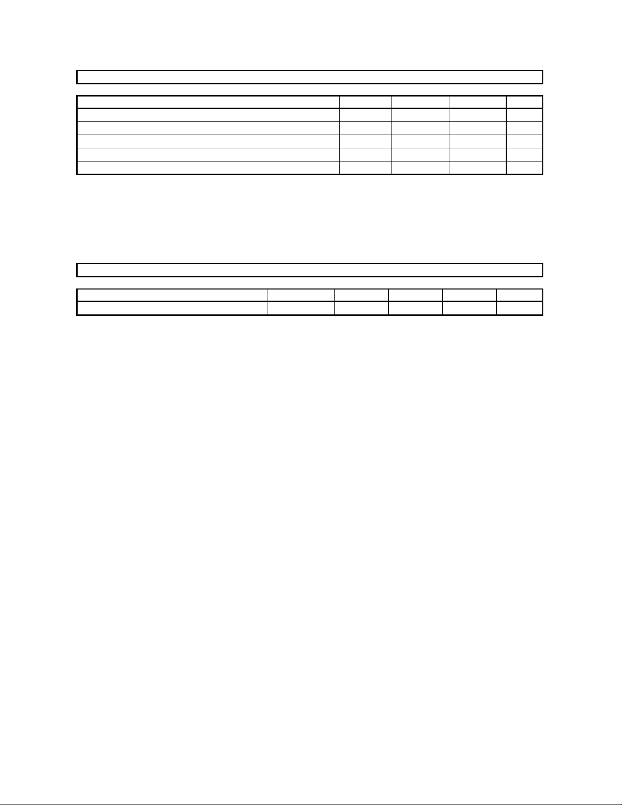
DC CHARACTERISTICS
(Ta=25°C; VDD=2.2 ∼ 3.6V)
Parameter Symbol min typ max Units
High-Level Input Voltage
Low-Level Input Voltage
Input Leakage Current Iin - -
VIH
VIL
70%VDD
-
-
-
-
30%VDD
±
10
V
V
µ
A
MS0280-E-00 2003/12
- 6 -

ASAHI KASEI [AK4386]
SWITCHING CHARACTERISTICS
(Ta=25°C; VDD=2.2 ∼ 3.6V)
Parameter Symbol min typ max Units
Master Clock Frequency
Half Speed Mode (512/768/1024/1536fs)
Normal Speed Mode (256/384/512/768fs)
Double Speed Mode (128/192/256/384fs)
Duty Cycle
LRCK Frequency
Half Speed Mode (DFS1-0 = “10”)
Normal Speed Mode (DFS1-0 = “00”)
Double Speed Mode (DFS1-0 = “01”)
Duty Cycle
Audio Interface Timing
BICK Period
Half Speed Mode
Normal Speed Mode
Double Speed Mode
BICK Pulse Width Low
Pulse Width High
BICK “↑” to LRCK Edge (Note 8)
LRCK Edge to BICK “↑” (Note 8)
SDTI Hold Time
SDTI Setup Time
Power-Down & Reset Timing
PDN Pulse Width (Note 9)
Note 8. BICK rising edge must not occur at the same time as LRCK edge.
Note 9. The AK4386 can be reset by bringing PDN pin = “L”.
The PDN pulse width is proportional to the value of the capacitor (C) connected to VCOM pin. tPD = 4 × C.
When C = 4.7µF, tPD is 19ms(min).
The value of the capacitor (C) connected with VCOM pin should be 1µF ≤ C ≤ 10 µF.
When the states of DIF1-0 pins change, the AK4386 should be reset by PDN pin.
fCLK
fCLK
fCLK
dCLK
fsh
fsn
fsd
dCLK
tBCK
tBCK
tBCK
tBCKL
tBCKH
tBLR
tLRB
tSDH
tSDS
tPD
4.096
2.048
6.144
40
8
8
48
45
1/128fs
1/128fs
1/64fs
70
70
40
40
40
40
4 × C
36.864
36.864
36.864
60
24
48
96
55
MHz
MHz
MHz
%
kHz
kHz
kHz
%
ns
ns
ns
ns
ns
ns
ns
ns
ns
ms
MS0280-E-00 2003/12
- 7 -

ASAHI KASEI [AK4386]
n Timing Diagram
1/fCLK
MCLK
tCLKH
tCLKL
VIH
VIL
1/fs
LRCK
VIH
VIL
tBCK
BICK
tBCKH
tBCKL
VIH
VIL
Clock Timing
LRCK
tBLR
tLRB
VIH
VIL
BICK
SDTI
tSDS
tSDH
VIH
VIL
VIH
VIL
Audio Interface Timing
tPD
PDN
VIL
Power Down & Reset Timing
MS0280-E-00 2003/12
- 8 -

ASAHI KASEI [AK4386]
OPERATION OVERVIEW
n
System Clock
The external clocks, which are required to operate the AK4386, are MCLK, BICK and LRCK. The master clock (MCLK)
should be synchronized with LRCK but the phase is not critical. The MCLK is used to operate the digital interpolation
filter and the delta-sigma modulator. The MCLK frequency is detected from the relation between MCLK and LRCK
automatically. The Half speed, the Normal speed and the Double speed mode are selected with the DFS1-0 pins (Table 1).
The sampling speed mode is set depending on the MCLK frequency automatically for Auto mode (DFS1 pin = DFS0 pin
= “H”) (Table 2).
The AK4386 is automatically placed in the power save mode when MCLK stops in the normal operation mode (PDN pin
= “H”), and the analog output becomes the VCOM voltage. After MCLK is input again, the AK4386 is powered up. After
exiting reset at power-up etc., the AK4386 is in the power-down mode until MCLK and LRCK are input.
When the states of DIF1-0 pins change in the normal operation mode, the AK4386 should be reset by PDN pin.
Mode DFS1 DFS0 fs MCLK Frequency
Normal Speed L L
Double Speed L H
Half Speed H L
Auto H H
Table 1. System Clock Example
MCLK Frequency Sampling Speed Mode fs
512/768fs Normal Speed
128/192/256/384fs Double Speed
1024/1536fs Half Speed
Table 2. Auto Mode
8 ∼ 48kHz
48 ∼ 96kHz
8 ∼ 24kHz
8 ∼ 96kHz
256/384/512/768fs
128/192/256/384fs
512/768/1024/1536fs
Table 2
8 ∼ 48kHz
48 ∼ 96kHz
8 ∼ 24kHz
n Audio Interface Format
Data is shifted in via the SDTI pin using BICK and LRCK inputs. The DIF1-0 pins as shown in Table 3 can select four
serial data modes. In all modes the serial data is MSB-first, 2’s compliment format and is latched on the rising edge of
BICK. Mode 3 can be used for 16bit I2S Compatible format by zeroing the unused LSBs at BICK ≥ 48fs or BICK = 32fs.
Mode DIF1 DIF0 SDTI Format BICK Figure
0 L L 16bit, LSB justified
1 L H 24bit, LSB justified
2 H L 24bit, MSB justified
3 H H 16/24bit, I2S Compatible
Table 3. Audio Interface Format
≥ 32fs
≥ 48fs
≥
48fs
≥ 48fs or 32fs
Figure 1
Figure 2
Figure 3
Figure 4
MS0280-E-00 2003/12
- 9 -

ASAHI KASEI [AK4386]
LRCK
0 1 102 3 9 11 12 13 14 15 0 1 2 3 10109 11 12 13 14 15
BICK(32fs)
SDTI(i)
15 14 13 7 6 5 4 3 2 1 0 15 14 13 157 6 5 4 3 2 1 0
0 1 182 3 19 20 31 0 1 2 3 1018 19 20 3117 17
BICK(64fs)
SDTI(i)
Don't Care 1 0 15 14 13 2 1 015 14 13 12 12Don't Care
SDTI-15:MSB, 0:LSB
Lch Data Rch Data
Figure 1. Mode 0 Timing
LRCK
0 1 2 24 31 0 1 2 1031248 9 8 9
BICK(64fs)
SDTI(i)
Don't Care 0 8 1 0
23:MSB, 0:LSB
23 8 Don't Care 231
Lch Data Rch Data
Figure 2. Mode 1 Timing
LRCK
0 1 2 20 21 24 31 0 1 2 102220 21 312422 23 23
BICK(64fs)
SDTI(i)
Don't Care0 0
23:MSB, 0:LSB
Lch Data Rch Data
Don't Care4 3 2 123 22 23 22 231234
Figure 3. Mode 2 Timing
LRCK
0 1 2 2521 24 0 1 2 1022 2521 2422 23 233
BICK(64fs)
SDTI(i)
Don't Care0 0
23:MSB, 0:LSB
Lch Data Rch Data
Don't Care4 3 2 123 22 23 22 1234
Figure 4. Mode 3 Timing
MS0280-E-00 2003/12
- 10 -

ASAHI KASEI [AK4386]
n De-emphasis Filter
The AK4386 includes the digital de-emphasis filter (tc=50/15µs) by IIR filter. This filter corresponds to 44.1kHz
sampling. The de-emphasis filter is enabled by setting DEM pin “H”. In case of Half speed and Double speed mode, the
digital de-emphasis filter is always off.
Mode DFS1 pin DFS0 pin DEM pin De-emphasis Filter
Normal Speed
Double Speed L H * OFF
Half Speed H L * OFF
Auto
Note. The digital de-emphasis filter corresponds to 44.1kHz sampling.
In case of Half speed and Double speed mode, the digital de-emphasis filter is always off.
L L L OFF
L L H ON
H H L OFF
H H H ON (Note)
Table 4. De-emephasis Filter (*: Don’t care)
n Power-down
The AK4386 is placed in the power-down mode by bringing PDN pin = “L”. and the digital filter is reset at the same time.
This reset should always be done after power up.
When PDN pin = “L”, DAC outputs go to Hi-Z. Also, the internal power down is automatically done when MCLK stops
during operating (PDN pin =“H”), and the analog outputs go to the VCOM voltage. MCLK pin should be fixed to “H” or
“L” when MCLK stops.
Mode PDN pin MCLK DAC Output State
0 L Don’t care Hi-Z Full Power Down
1 Supplied Normal Output Normal
2
H
Not Supplied VCOM Voltage Power Save
Table 5. Power down mode
MS0280-E-00 2003/12
- 11 -

ASAHI KASEI [AK4386]
(1) Power down by PDN pin
PDN
(1)
Internal
State
Normal Operation
Power-down Normal Operation
D/A In
(Digital)
D/A Out
(Analog)
Clock In
MCLK, BICK, LRCK
External
MUTE
GD GD
(2)
(4)
(6)
“0” data
(5)
Don’t care
Mute ON
(3)
(4)
(2)
Notes:
(1) PDN pin should be “L” for 19ms or more when an electrolytic capacitor 4.7µF is attached between VCOM pin and
VSS.)
(2) The analog output corresponding to digital input has the group delay (GD).
(3) When PDN pin = “L”, the analog output is Hi-Z.
(4) Click noise occurs in 3 ∼ 4LRCK at both edges (↑ ↓) of PDN signal. This noise is output even if “0” data is input.
(5) The external clocks (MCLK, BICK and LRCK) can be stopped in the power down mode (PDN pin = “L”).
(6) Please mute the analog output externally if the click noise (4) influences system application. The timing example
is shown in this figure.
Figure 5. Power-down/up sequence example 1
MS0280-E-00 2003/12
- 12 -

ASAHI KASEI [AK4386]
(2) Power save by MCLK stop (PDN pin = “H”)
PDN pin
(1)
Internal
State
D/A In
(Digital)
D/A Out
(Analog)
Clock In
MCLK, BICK, LRCK
External
MUTE
Power-down
Power-down
Hi-Z
Normal Operation
(4)
(5)
Power-save Normal Operation
(3)
GD GD
(2)
(6)
(4)
(5)
VCOM
MCLK Stop
(4)
(6)
(2)
Notes:
(1) PDN pin should be “L” for 19ms or more when an electrolytic capacitor 4.7µF is attached between VCOM pin and
VSS.)
(2) The analog output corresponding to digital input has the group delay (GD).
(3) The digital data can be stopped. The click noise after MCLK is input again by inputting the “0” data to this section
can be reduced.
(4) Click noise occurs in 3 ∼ 4LRCK at both edges (↑ ↓) of PDN signal, MCLK inputs and MCLK stops. This noise is
output even if “0” data is input.
(5) The external clocks (BICK and LRCK) can be stopped in the power down mode (MCLK stop).
(6) Please mute the analog output externally if the click noise (4) influences system application. The timing example
is shown in this figure.
Figure 6. Power-down/up sequence example 2
MS0280-E-00 2003/12
- 13 -

ASAHI KASEI [AK4386]
VSS
+
Lch Out
+
SYSTEM DESIGN
Figure 7 shows the system connection diagram. An evaluation board is available which demonstrates application circuits,
the optimum layout, power supply arrangements and measurement results.
Master Clock
64fs
24bit Audio Data
fs
Reset & Power down
Mode
Setting
Analog Ground Digital Ground
MCLK
1
BICK
2
SDTI
3
LRCK
4
PDN 5
DFS0
6
DFS1
7
DEM 8
AK4386
TEST
DIF1
VDD 14
VCOM
LOUT 11
ROUT
DIF0
16
15
13
12
10
Analog Supply
10u
0.1u
4.7u
(C)
Rch Out
9
2.2 to 3.6V
Note:
- VSS of the AK4386 should be distributed separately from the ground of external digital devices (MPU, DSP etc.).
- When AOUT drive some capacitive load, some resistor should be added in series between AOUT and capacitive
load.
- The value of the capacitor connected to VCOM pin should be 1µF ≤ C ≤ 10µF.
- All digital input pins should not be left floating.
Figure 7. Typical Connection Diagram
1. Grounding and Power Supply Decoupling
The AK4386 requires careful attention to power supply and grounding arrangements. VDD is usually supplied from the
analog supply in the system. System analog ground and digital ground should be connected together near to where the
supplies are brought onto the printed circuit board. Decoupling capacitors should be as near to the AK4386 as possible,
with the small value ceramic capacitor being the closest.
2. Voltage Reference
The differential Voltage between VDD and VSS sets the analog output range. VCOM is used as a common voltage of the
analog signal. VCOM pin is a signal ground of this chip. An electrolytic capacitor about 4.7µF should be attached
between VCOM pin and VSS. No load current may be drawn from VCOM pin. Especially, the ceramic capacitor should
be connected to this pin as near as possible.
3. Analog Outputs
The analog outputs are single-ended and centered around the VCOM voltage (0.55 × VDD). The output signal range is
typically 2.0Vpp (typ@VDD=3.0V). The internal switched-capacitor filter and continuous-time filter attenuate the noise
generated by the delta-sigma modulator beyond the audio passband. The output voltage is a positive full scale for
7FFFFFH (@24bit) and a negative full scale for 800000H (@24bit). The ideal output is VCOM voltage (0.55 × VDD) for
000000H (@24bit).
DC offsets on analog outputs are eliminated by AC coupling since analog outputs have DC offsets of VCOM + a few mV.
MS0280-E-00 2003/12
- 14 -

ASAHI KASEI [AK4386]
0.1±0.1
0∼10
°
Seating Plane
0.10
0.17±0.05
0.22±0.1
0.65
5.0
1.10max
A18916
16pin TSSOP (Unit: mm)
4.4
6.4
±
0.2
0.5
±
0.2
PACKAGE
Detail A
n Material & Lead finish
Package molding compound: Epoxy
Lead frame material: Cu
Lead frame surface treatment: Solder (Pb free) plate
MS0280-E-00 2003/12
- 15 -

ASAHI KASEI [AK4386]
MARKING
AKM
4386VT
XXYYY
1) Pin #1 indication
2)
Date Code : XXYYY (5 digits)
XX: Lot#
YYY: Date Code
3) Marketing Code : 4386VT
IMPORTANT NOTICE
•
These products and their specifications are subject to change without notice. Before considering any
use or application, consult the Asahi Kasei Microsystems Co., Ltd. (AKM) sales office or authorized
distributor concerning their current status.
•
AKM assumes no liability for infringement of any patent, intellectual property, or other right in the
application or use of any information contained herein.
• Any export of these products, or devices or systems containing them, may require an export license
or other official approval under the law and regulations of the country of export pertaining to customs
and tariffs, currency exchange, or strategic materials.
• AKM products are neither intended nor authorized for use as critical components in any safety, life
support, or other hazard related device or system, and AKM assumes no responsibility relating to any
such use, except with the express written consent of the Representative Director of AKM. As used
here:
a. A hazard related device or system is one designed or intended for life support or maintenance of
safety or for applications in medicine, aerospace, nuclear energy, or other fields, in which its
failure to function or perform may reasonably be expected to result in loss of life or in significant
injury or damage to person or property.
b. A critical component is one whose failure to function or perform may reasonably be expected to
result, whether directly or indirectly, in the loss of the safety or effectiveness of the device or
system containing it, and which must therefore meet very high standards of performance and
reliability.
• It is the responsibility of the buyer or distributor of an AKM product who distributes, disposes of, or
otherwise places the product with a third party to notify that party in advance of the above content and
conditions, and the buyer or distributor agrees to assume any and all responsibility and liability for
and hold AKM harmless from any and all claims arising from the use of said product in the absence of
such notification.
MS0280-E-00 2003/12
- 16 -
 Loading...