

Page 1
ASAHI KASEI [AK4382]
AK4382
DS
112dB 192kHz 24-Bit 2ch
GENERAL DESCRIPTIO N
The AK4382 offers the perfect mix for cost and performance based audio systems. Using AKM's multi bit
architecture for its modulator the AK4382 delivers a wide dynamic range while preserving linearit y for
improved THD+N performance. The AK4382 has full differential SCF outputs, removing the need for AC
coupling capacitors and increasing performance for systems with excessive clock jitter. The 24 Bit word
length and 192kHz sampling rate make this part ideal for a wide range of applications including DVDAudio. The AK4382 is offered in a space saving 16pin TSSOP package.
FEATURES
o Sampling Rate Ranging from 8kHz to 192kHz
o 128 times Oversampling (Normal Speed Mode)
o 64 times Oversampling (Double Speed Mode)
o 32 times Oversampling (Quad Speed Mode)
o 24-Bit 8 times FIR Digital Filter
o On chip SCF
o Digital de-emphasis for 32k, 44.1k and 48kHz sampling
o Soft mute
o Digital Attenuator (256 steps)
o I/F format: 24-Bit MSB justified, 24/20/16-Bit LSB justified or I
o Master clock: 256fs, 384fs, 512fs or 768fs (Normal Speed Mode)
128fs, 192fs, 256fs or 384fs (Double Speed Mode)
128fs, 192fs (Quad Speed Mode)
o THD+N: -94dB
o Dynamic Range: 112dB
o High Tolerance to Clock Jitter
o Power supply: 4.75 to 5.25V
o Very Small Package: 16pin TSSOP (6.4mm x 5.0mm)
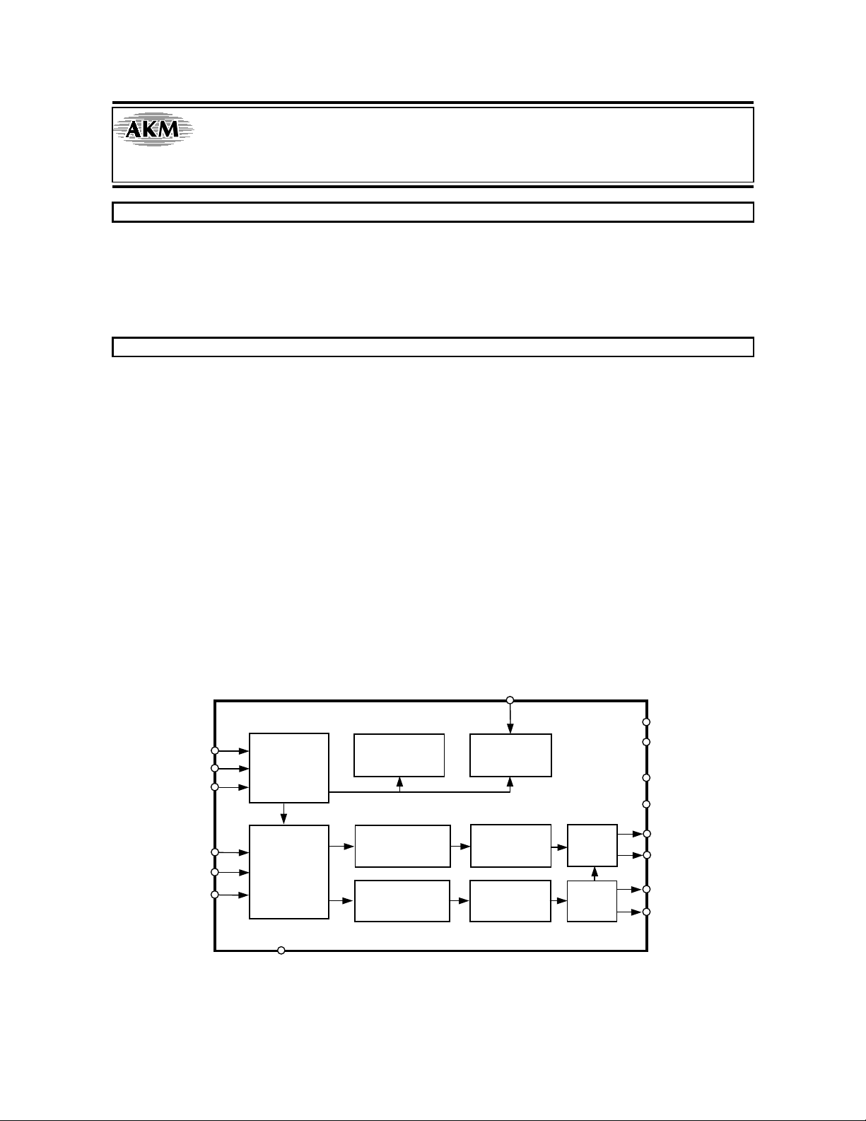
2
S
DAC
MCLK
VDD
CSN
CCLK
CDTI
LRCK
BICK
SDTI
MS0034-E-00 2000/7
µP
Interface
Audio
Data
Interface
PDN
De-emphasis
Control
8X
Interpolator
8X
Interpolator
- 1 -
Clock
Divider
DS
Modulator
DS
Modulator
SCF
SCF
VSS
DZFL
DZFR
AOUTL+
AOUTL-
AOUTR+
AOUTR-
Page 2
ASAHI KASEI [AK4382]
n Ordering Guide
AK4382VT -40 ~ +85°C 16pin TSSOP (0.65mm pitch)
AKD4382 Evaluation Board for AK4382
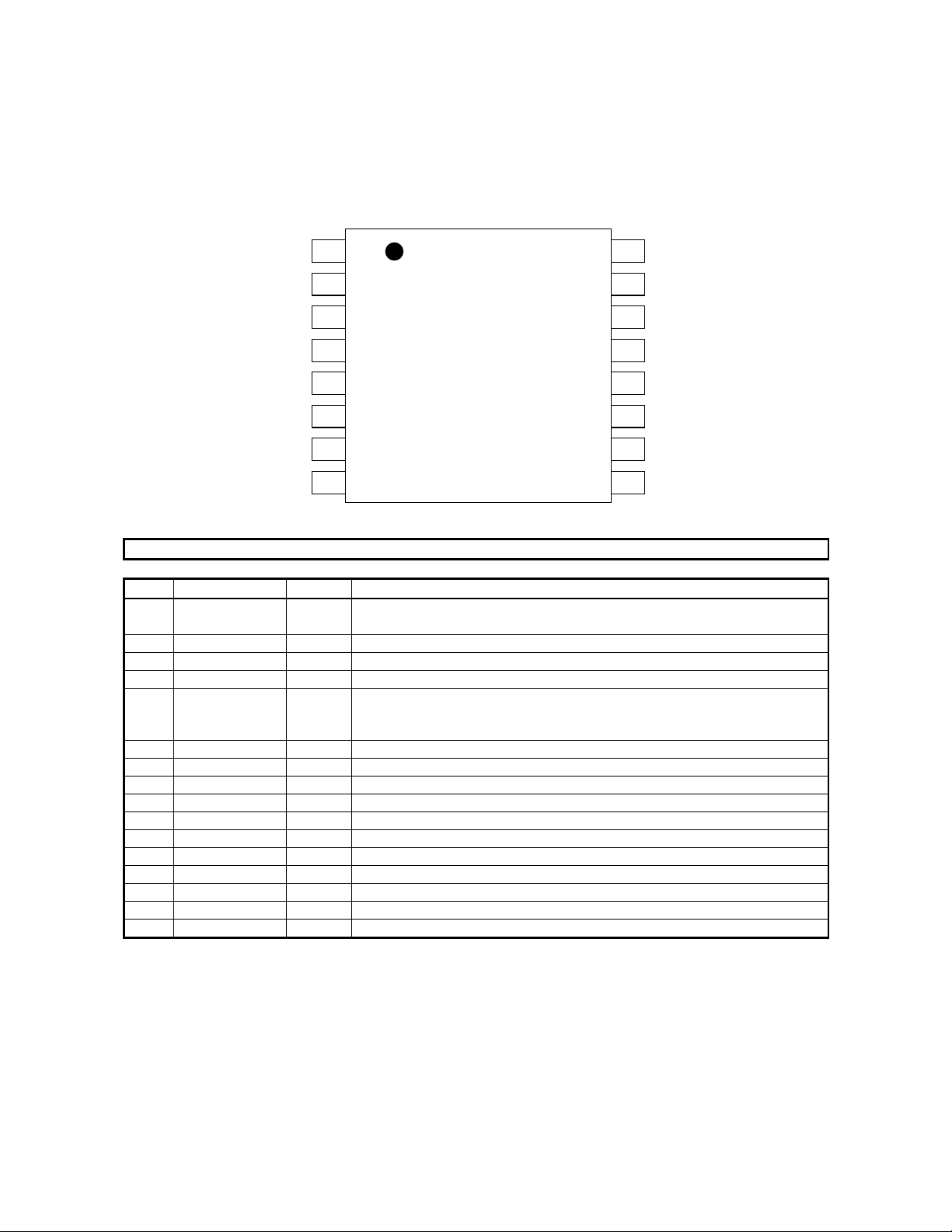
n Pin Layout
MCLK
BICK
SDTI
LRCK
PDN
CSN
CCLK
CDTI
1
2
3
4
5
6
7
8
Top
View
PIN/FUNCTION
No. Pin Name I/O Function
1 MCLK I Master Clock Input Pin
An external TTL clock should be input on this pin.
2 BICK I Audio Serial Data Clock Pin
3 SDTI I Audio Serial Data Input Pin
4 LRCK I L/R Clock Pin
5 PDN I Power-Down Mode Pin
When at “L”, the AK4382 is in the power-down mode and is held in reset.
The AK4382 should always be reset upon power-up.
6 CSN I Chip Select Pin
7 CCLK I Control Data Input Pin
8 CDTI I Control Data Input Pin in serial mode
9 AOUTR- O Rch Negative Analog Output Pin
10 AOUTR+ O Rch Positive Analog Output Pin
11 AOUTL- O Lch Negative Analog Output Pin
12 AOUTL+ O Lch Positive Analog Output P in
13 VSS - Ground Pin
14 VDD - Power Supply Pin
15 DZFR O Rch Data Zero Input Detect Pin
16 DZFL O Lch Data Zero Input Detect Pin
Note: All input pins should not be left floating.
16
15
14
13
12
11
10
DZFL
DZFR
VDD
VSS
AOUTL+
AOUTL-
AOUTR+
9
AOUTR-
MS0034-E-00 2000/7
- 2 -
Page 3
ASAHI KASEI [AK4382]
ABSOLUTE MAXI MUM RATINGS
(VSS=0V; Note 1)
Parameter Symbol min max Units
Power Supply VDD -0.3 6.0 V
Input Current (any pins except for supplies) IIN Input Voltage VIND -0.3 VDD+0.3 V
Ambient Operating Temperature Ta -40 85
Storage Temperature Tstg -65 150
Note: 1. All voltages with respect to ground.
WARNING: Operation at or beyond these limits may results in permanent damage to the device.
Normal operation is not guaranteed at these extremes.
±10
mA
°C
°C
RECOMMENDED OPERATING CONDITIONS
(VSS=0V; Note 1)
Parameter Symbol min typ max Units
Power Supply VDD 4.75 5.0 5.25 V
*AKM assumes no responsibility for the usage beyond the conditions in this datasheet.
MS0034-E-00 2000/7
- 3 -
Page 4
ASAHI KASEI [AK4382]
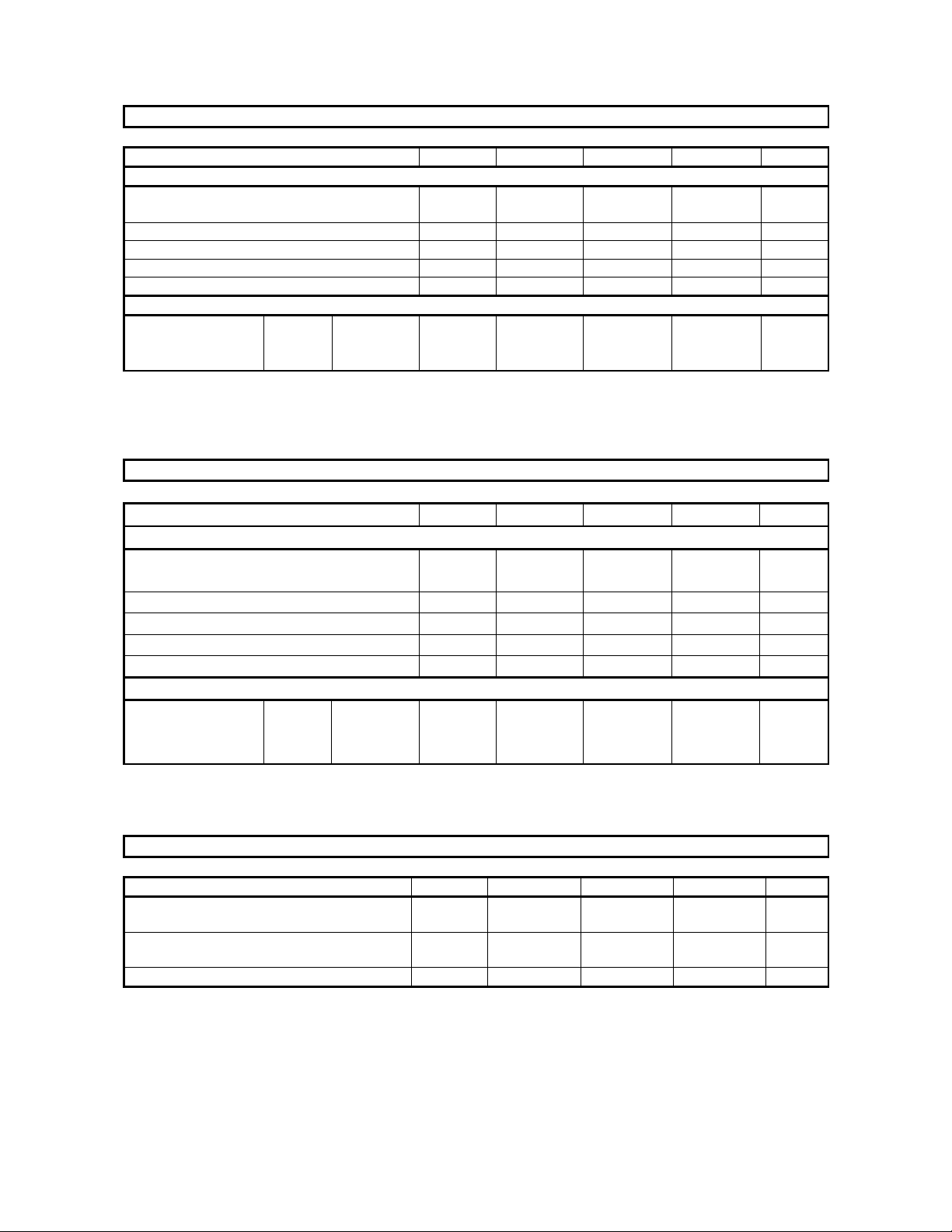
ANALOG CHARACTERISTICS
(Ta=25°C; VDD=5.0V; fs=44.1kHz; BICK=64fs; Signal Frequency=1kHz; 24bit Input Data;
Measurement frequency=20Hz ~ 20kHz; R
³2kW; unless otherwise specified)
L
Parameter min typ max Units
Resolution 24 Bits
Dynamic Characteristics (Note 3)
THD+N
fs=44.1kHz
BW=20kHz
fs=96kHz
BW=40kHz
fs=192kHz
BW=40kHz
0dBFS
-60dBFS
0dBFS
-60dBFS
0dBFS
-60dBFS
-94
-48
-92
-45
-92
-45
-86
-84
dB
-
dB
dB
-
-
-
dB
dB
dB
Dynamic Range (-60dBFS with A-weighted) (Note 4) 102 112 dB
S/N (A-weighted) (Note 5) 102 112 dB
Interchannel Isolation (1kHz) 90 110 dB
Interchannel Gain Mismatch 0.2 0.5 dB
DC Accuracy
Gain Drift 100 Output Voltage (Note 6)
±2.55 ±2.75 ±2.95
Load Resistance (Note 7) 2
ppm/°C
Vpp
kW
Power Supplies
Power Supply Current (VDD)
Normal Operation (PDN = “H”, fs£96kHz)
Normal Operation (PDN = “H”, fs=192kHz)
Power-Down Mode (PDN = “L”) (Note 8)
20
25
10
34
42
100
mA
mA
µA
Notes: 3. Measured by Audio Precision (System Two). Refer to the evaluation board manual.
4. 100dB at 16bit data.
5. S/N does not depend on input bit length.
6. Full-scale voltage (0dB). Output voltage scales with the voltage of VREF,
AOUT (typ.@0dB)=(AOUT+)-(AOUT-)=±2.75Vpp × VREF/5.
7. For AC-load. 4kW for DC-load.
8. All digital inputs including clock pins (MCLK, BICK and LRCK) are held VDD or VSS.
MS0034-E-00 2000/7
- 4 -
Page 5
ASAHI KASEI [AK4382]
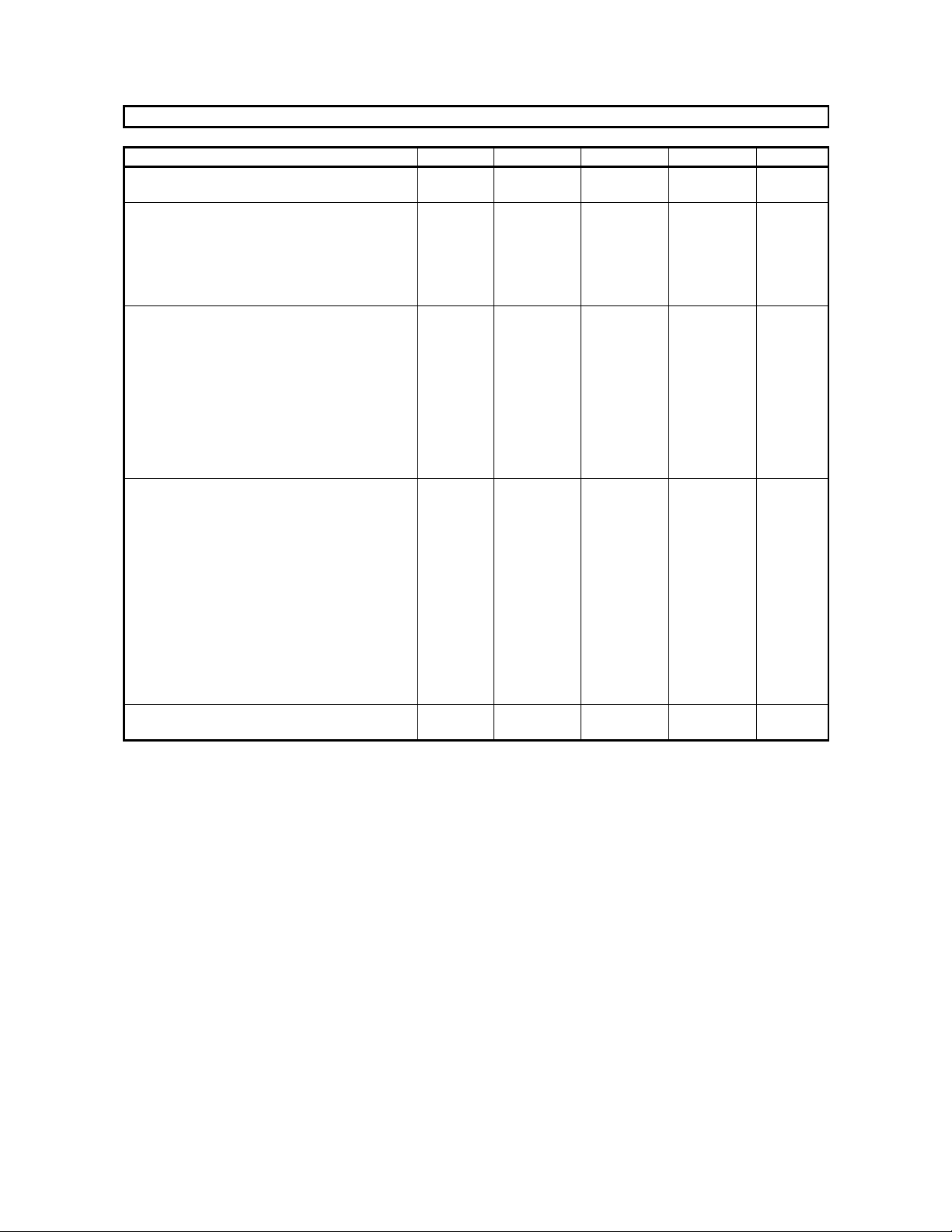
SHARP ROLL-OFF FILTER CHARACTERISTICS
(Ta = 25°C; VDD = 4.75 ~ 5.25V; fs = 44.1kHz; DEM = OFF; SLOW = “0”)
Parameter Symbol min typ max Units
Digital filter
Passband ±0.05dB (Note 9)
-6.0dB
Stopband (Note 9) SB 24.25 KHz
Passband Ripple PR
Stopband Attenuation SA 54 DB
Group Delay (Note 10) GD - 19.3 - 1/fs
Digital Filter + LPF
Frequency Response 20.0kHz
40.0kHz
80.0kHz
Notes: 9. The passband and stopband frequencies scale with fs(system sampling rate).
For example, PB=0.4535×fs (@±0.05dB), SB=0.546×fs.
10. The calculating delay time which occurred by digital filtering. This time is from setting the 16/24bit data
of both channels to input register to the output of analog signal.
fs=44.1kHz
fs=96kHz
fs=192kHz
PB 0
FR
FR
FR
- 22.05
-
-
-
± 0.2
± 0.3
+0/-0.6
20.0
-
± 0.02
-
-
-
KHz
KHz
DB
Db
dB
dB
SLOW ROLL-OFF FILTER CHA RACTERISTICS
(Ta = 25°C; AVDD, DVDD = 4.75~5.25V; fs = 44.1kHz; DEM = OFF; SLOW = “1”)
Parameter Symbol min typ max Units
Digital Filter
Passband ±0.04dB (Note 11)
-3.0dB
Stopband (Note 11) SB 39.2 kHz
Passband Ripple PR ± 0.005 dB
Stopband Attenuation SA 72 dB
Group Delay (Note 10) GD - 19.3 - 1/fs
Digital Filter + SCF
Frequency Response
Note: 11. The passband and stopband frequencies scale with fs.
For example, PB = 0.185×fs (@±0.04dB), SB = 0.888×fs.
20.0kHz
40.0kHz
80.0kHz
fs=44.kHz
fs=96kHz
fs=192kHz
PB 0
FR
FR
FR
- 18.2
-
-
-
+0/-5
+0/-4
+0/-5
8.1
kHz
-
-
-
-
kHz
dB
dB
dB
DC CHARACTERISTICS
(Ta=25°C; VDD=4.5 ~ 5.5V)
Parameter Symbol min typ max Units
High-Level Input Voltage
Low-Level Input Voltage
High-Level Output Voltage (Iout=-80µA)
Low-Level Output Voltage (Iout=80µA)
Input Leakage Current Iin - -
MS0034-E-00 2000/7
VIH
VIL
VOH
VOL
- 5 -
2.2
-
VDD-0.4
-
-
-
--
-
0.8
0.4
± 10
V
V
V
V
µA
Page 6
ASAHI KASEI [AK4382]
SWITCHING CHARACTERISTICS
(Ta=25°C; VDD=4.5 ~ 5.5V; CL=20pF)
Parameter Symbol min typ max Units
Master Clock Frequency
Duty Cycle
LRCK Frequency
Normal Speed Mode
Double Speed Mode
Quad Speed Mode
Duty Cycle
Audio Interface Timing
BICK Period
Normal Speed Mode
Double/Quad Speed Mode
BICK Pulse Width Low
Pulse Width High
BICK rising to LRCK Edge (Note 12)
LRCK Edge to BICK rising (Note 12)
SDTI Hold Time
SDTI Setup Time
Control Interface Timing
CCLK Period
CCLK Pulse Width Low
Pulse Width High
CDTI Setup Time
CDTI Hold Time
CSN “H” Time
CSN “¯” to CCLK “”
CCLK “” to CSN “”
Rise Time of CSN
Fall Time of CSN
Rise Time of CCLK
Fall Time of CCLK
Reset Timing
PDN Pulse Width (Note 13)
Notes: 12. BICK rising edge must not occur at the same time as LRCK edge.
13. The AK4382 can be reset by bringing PDN= “L”.
fCLK
dCLK
fsn
fsd
fsq
Duty
tBCK
tBCK
tBCKL
tBCKH
tBLR
tLRB
tSDH
tSDS
tCCK
tCCKL
tCCKH
tCDS
tCDH
tCSW
tCSS
tCSH
tR1
tF1
tR2
tF2
tPD 100 ns
2.048
40
8
60
120
45
1/128fs
1/64fs
30
30
20
20
20
20
200
80
80
40
40
150
50
50
11.2896 36.864
60
48
96
192
55
20
20
20
20
MHz
%
kHz
kHz
kHz
%
ns
ns
ns
ns
ns
ns
ns
ns
ns
ns
ns
ns
ns
ns
ns
ns
ns
ns
ns
ns
MS0034-E-00 2000/7
- 6 -
Page 7
ASAHI KASEI [AK4382]
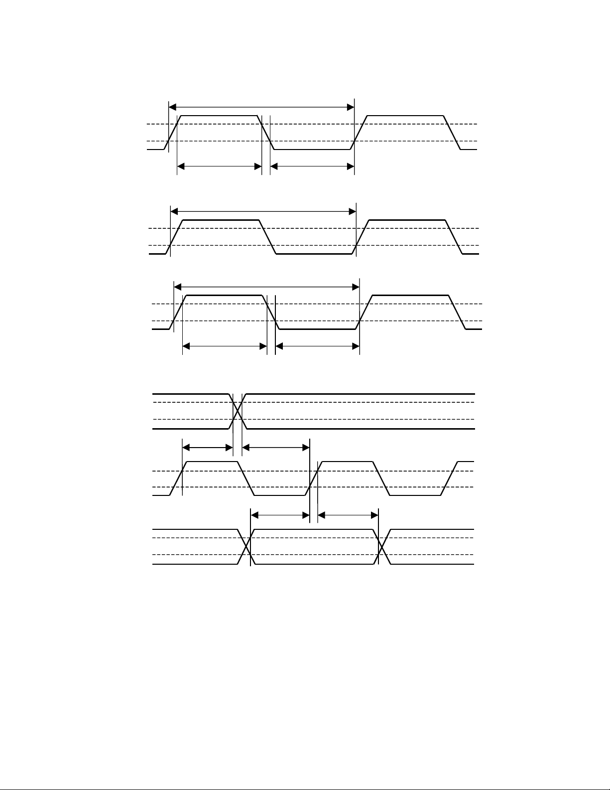
n Timing Diagram
1/fCLK
MCLK
LRCK
BICK
LRCK
tCLKH
tBCKH
1/fs
tBCK
Clock Timing
tCLKL
tBCKL
VIH
VIL
dCLK=tCLKH x fCLK, tCLKL x fCLK
VIH
VIL
VIH
VIL
VIH
VIL
BICK
SDTI
tBLR
tLRB
tSDS
tSDH
Serial Interface Timing
VIH
VIL
VIH
VIL
MS0034-E-00 2000/7
- 7 -
Page 8

ASAHI KASEI [AK4382]
VIH
CSN
VIL
CCLK
CDTI
CSN
CCLK
tCSS
C1 C0 R/W A4
tCCKL tCCKH
tCDS tCDH
WRITE Command Input Timing
VIH
VIL
VIH
VIL
tCSW
VIH
VIL
tCSH
VIH
VIL
CDTI
D3 D2 D1 D0
VIH
VIL
WRITE Data Input Timing
tPD
PDN
VIL
Power-down Timing
MS0034-E-00 2000/7
- 8 -
Page 9

ASAHI KASEI [AK4382]
OPERATION OVERVI EW
n System Clock
The external clocks, which are required to operate the A K4382, are MCL K, L RCK an d BICK. The m aster clock (MCL K)
should be synchronized with LRCK but the phase is not critical. The MCLK is used to operate the digital interpolation
filter and the delta-sigma modulator. There are two methods to set MCLK frequency. In Manual Setting Mode (ACKS =
“0”: Register 00H), the sampling speed is set by DFS0/1(Table 1). The frequency of MCLK at each sampling speed is set
automatically. (Table 2~4). In Auto Setting Mode (ACKS = “1”: Default), as MCLK frequency is detected automatically
(Table 5), and the internal master clock becomes the appropriate frequency (Table 6), it is no t necessary to set DFS0/1.
All external clocks (MCLK,BIC K an d LRCK) should always be present wh en ev er th e A K4382 is in the normal operation
mode (PDN= ”H”). If these clocks are not provided, the AK4382 may draw excess current because the device utilizes
dynamic refreshed logic internally. The AK4382 should be reset by PDN= “L” after threse clocks are provided. If the
external clocks are not present, the AK4382 should be in the power-down mode (PDN= “L”). After exiting reset at
power-up etc., the AK4382 is in the power-down mode until MCLK and LRCK are input.
DFS1 DFS0 Sampling Rate (fs)
0 0 Normal Speed Mode 8kHz~48kHz
0 1 Double Speed Mode 60kHz~96kHz
1 0 Quad Speed Mode 120kHz~192kHz
Default
Table 1. Sampling Speed (Manual Setting Mode)
LRCK MCLK BICK
fs 256fs 384fs 512fs 768fs 64fs
32.0kHz 8.1920MHz 12.2880MHz 16.3840MHz 24.5760MHz 2.0480MHz
44.1kHz 11.2896MHz 16.9344MHz 22.5792MHz 33.8688MHz 2.8224MHz
48.0kHz 12.2880MHz 18.4320MHz 24.5760MHz 36.8640MHz 3.0720MHz
Table 2. System Clock Example (Normal Speed Mode @Manual Setting Mode)
LRCK MCLK BICK
fs 128fs 192fs 256fs 384fs 64fs
88.2kHz 11.2896MHz 16.9344MHz 22.5792MHz 33.8688MHz 5.6448MHz
96.0kHz 12.2880MHz 18.4320MHz 24.5760MHz 36.8640MHz 6.1440MHz
Table 3. System Clock Example (Double Speed Mode @Manual Setting Mode)
LRCK MCLK BICK
fs 128fs 192fs 64fs
176.4kHz 22.5792MHz 33.8688MHz 11.2896MHz
192.0kHz 24.5760MHz 36.8640MHz 12.2880MHz
Table 4. System Clock Example (Quad Speed Mode @Manual Setting Mode)
MS0034-E-00 2000/7
- 9 -
Page 10

ASAHI KASEI [AK4382]
MCLK Sampling Speed
512fs 768fs Normal
256fs 384fs Double
128fs 192fs Quad
Table 5. Sampling Speed (Auto Setting Mode)
LRCK MCLK (MHz)
fs 128fs 192fs 256fs 384fs 512fs 768fs
32.0kHz - - - - 16.3840 24.5760
44.1kHz - - - - 22.5792 33.8688
48.0kHz - - - - 24.5760 36.8640
88.2kHz - - 22.5792 33.8688 - -
96.0kHz - - 24.5760 36.8640 - -
176.4kHz 22.5792 33.8688 - - - -
192.0kHz 24.5760 36.8640 - - - -
Table 6. System Clock Example (Auto Setting Mode)
Sampling Speed
Normal
Double
Quad
n Audio Serial Interface Format
Data is shifted in via the SDTI pin using BI CK and LRCK inp uts. T he DIF0-2 as shown in T able 7 can select five serial
data modes. In all modes the serial data is MSB-first, 2’s compliment format and is latched on the rising edge o f BICK.
Mode 2 can be used for 16/20 MSB justified formats by zeroing the unused LSBs.
Mode DIF2 DIF1 DIF0 SDTI Format BICK Figure
0 0 0 0 16bit LSB Justified
1 0 0 1 20bit LSB Justified
2 0 1 0 24bit MSB Justified
3 0 1 1 24bit I2S Compatible
4 1 0 0 24bit LSB Justified
³32fs
³40fs
³48fs
³48fs
³48fs
Figure 1
Figure 2
Figure 3
Figure 4
Figure 2
Default
Table 7. Audio Data Formats
MS0034-E-00 2000/7
- 10 -
Page 11

ASAHI KASEI [AK4382]
(
)
(
)
(
)
(
)
LRCK
0 1 10 11 12 13 14 15 0 1 10 11 12 13 14 15 0 1
BICK
32fs
SDTI
Mode 0
BICK
64fs
SDTI
Mode 0
LRCK
BICK
64fs
SDTI
Mode 1
SDTI
Mode 4
15 14 6 5 4
1
014
Don’t care
15:MSB, 0:LSB
3210 1514
15 16 17 31 0 1
15 14 0
15 14 6 5 4 3 2 1 0
14
15 16 17 31 0 1
Don’t care
15 14 0
Lch Data Rch Data
Figure 1. Mode 0 Timing
091 10 11 12 31 0 1 9 10 11 12 31 0 1
Don’t care Don’t care
19:MSB, 0:LSB
Don’t care
23:MSB, 0:LSB
8
19 0
23 23
22 21 22 21
20 19 0
Don’t care
8
19 0
20 19 0
Lch Data Rch Data
Figure 2. Mode 1,4 Timing
LRCK
0221 2 24 31 0 1 31 0 1
23 30 2222423 30
BICK
64fs
SDTI
22 1 0 Don’t care23
23:MSB, 0:LSB
22 1
23
0 Don’t car e
2223
Lch Data Rch Data
Figure 3. Mode 2 Timing
MS0034-E-00 2000/7
- 11 -
Page 12

ASAHI KASEI [AK4382]
(
)
LRCK
031 2 24 31 0 1 31 0 1
23 25 322423 25
BICK
64fs
SDTI
22
23
23:MSB, 0:LSB
0
1
Don’t care
22 1
0
Don’t care23
23
Lch Data Rch Data
Figure 4. Mode 3 Timing
n De-emphasis Filter
A digital de-emphasis filter is available for 32, 44.1 or 48kHz sampling rates (tc = 50/15µs) and is enabled or disabled with
DEM0 and DEM1. In case of double speed and quad speed mode, the digital de -emphasis filter is always off.
DEM1 DEM0 Mode
0 0 44.1kHz
01OFF
Default
1 0 48kHz
1 1 32kHz
Table 8. De-emphasis Filter Control (Normal Speed Mode)
n
n Output Volume
nn
The AK4382 includes channel independent dig ital ou tpu t v olumes (ATT) with 256 levels at linear step in clu ding MUTE.
These volumes are in front of the DAC and can attenuate the input data from 0dB to –48dB and mute. When changing
levels, transitions are executed via soft changes; thus no switching noise occurs during these transitions. The transition time
of 1 level and all 256 levels is shown in Table 9.
Sampling Speed
Transition Time
1 Level 255 to 0
Normal Speed Mode 4LRCK 1020LRCK
Double Speed Mode 8LRCK 2040LRCK
Quad Speed Mode 16LRCK 4080LRCK
Table 9. ATT Transition Time
MS0034-E-00 2000/7
- 12 -
Page 13

ASAHI KASEI [AK4382]
n Zero Detection
The AK4382 has channel-independent zeros detect function . When the input data at each channel is continuous ly zeros for
8192 LRCK cycles, DZF pin of each ch an n el g oes to “ H”. DZ F pin of each ch an n el immediately goes to “L” if input data
of each channel is n ot zero after goin g DZ F “H”. If RSTN bit is “ 0”, DZF pin s of both channels go to “ H”. DZF pin of both
channels go to “L” at 2~3/fs after RSTN bit returns to “1”. If DZFM bit is set to “1”, DZF pins of both channels go to “H”
only when the input data at both channels are continuously zeros for 8192 LRCK cycles. Zero detect function can be
disabled by DZFE bit. In this case, DZF pins of both chann els are alway s “L”. DZFB bit can invert the polarity of DZF pin.
n Soft Mute Operation
Soft mute operation is performed at digital domain. When the SMUTE bit goes to “1”, the output signal is attenuated by -¥
during ATT_DATA´ATT transition time (Table 9) from the current ATT level. When the SMUTE bit is returned to “0”,
the mute is cancelled and the output attenuation gradually changes to the ATT level during ATT_DATA´ATT transition
time. If the soft mute is cancelled before attenuating to -¥ after starting the operation, the attenuation is discontinued and
returned to ATT level by the same cycle. The soft mute is effective for changing the signal source without stopping the
signal transmission.
SMUTE bit
ATT Level
Attenuation
-
¥
AOUT
DZF pin
Notes:
(1) ATT_DATA´ATT transition time (Table 9). For example, in Normal Speed Mode, this time is 1020LRCK cycles
(1020/fs) at ATT_DATA=255.
(2) The analog output corresponding to the digital input has a group delay, GD.
(3) If the soft mute is cancelled before attenuating to -¥ after starting the operation, the attenuation is discontinued and
returned to ATT level by the same cycle.
(4) When the input data at each chann el is contin u ou sly zeros for 8192 LRCK cycles, DZF pin of each ch an n el g oes to
“H”. DZF pin immediately goes to “L” if input data are not zero after going DZF “H”.
(1)
GD
(2)
(4)
8192/fs
Figure 5. Soft Mute and Zero Detection
(1)
(3)
GD
MS0034-E-00 2000/7
- 13 -
Page 14

ASAHI KASEI [AK4382]
n System Reset
The AK4382 should be reset once by bringing PDN= ”L” upon power-up. The AK4382 is powered up and the internal
timing starts clocking by LRCK “” after exiting reset and power dow n state by MCL K. The AK4382 is in the pow er-down
mode until MCLK and LRCK are input.
n Power-down
The AK4382 is placed in the power-dow n m ode by bringi ng PDN pin “L ” and the anlog ou tputs are floatin g (Hi-Z). Figu re
6 shows an example of the system timing at the power-down and power-up.
PDN
Internal
State
D/A In
(Digital)
D/A Out
Normal Operation
GD
(1)
Power-down Normal Operation
“0” data
(3)
(2)
(3)
GD
(Analog)
(4)
Clock In
MCLK, LRCK, BICK
DZFL/DZFR
External
MUTE
(5)
Don’t care
(6)
Mute ON
Notes:
(1) The analog output corresponding to digital input has the group delay (GD).
(2) Analog outputs are floating (Hi -Z) at the power-down mode.
(3) Click noise occurs at the edge of PDN signal. This noise is output even if “0” data is input.
(4) The external clocks (MCLK, BICK and LRCK) can be stopped in the power-down mode (PDN = “L”).
(5) Please mute the analog output externally if the click noise (3) influences system application.
The timing example is shown in this figure.
(6) DZF pins are “L” in the power-down mode (PDN = “L”).
(1)
Figure 6. Power-down/up Sequence Example
MS0034-E-00 2000/7
- 14 -
Page 15

ASAHI KASEI [AK4382]
n
n Reset Function
nn
When RSTN=0, DAC is powered down but the internal register values are not initialized. The analog outputs go to VCOM
voltage and DZF pin goes to “H”. Figure 7 shows the example of reset by RSTN bit.
RSTN bit
Internal
2~3/fs (6)3~4/fs (6)
RSTN bit
Internal
State
D/A In
(Digital)
D/A Out
Normal Operation
(1)
GD GD
Digital Block Power-down
“0” data
(3)
(2)
Normal Operation
(1)
(3)
(Analog)
(4)
Clock In
MCLK,LRCK,BICK
Don’t care
2/fs(5)
DZF
Notes:
(1) The analog output corresponding to digital input has the group delay (GD).
(2) Analog outputs go to VCOM voltage (VDD/2).
(3) Click noise occurs at the edges(“ ¯”) of the internal timing of RSTN bit. This noise is output even if “0” data is
input.
(4) The external clocks (MCLK, BICK and LRCK) can be stopped in the reset mode (RSTN = “L”).
(5) DZF pins go to “H” when the RSTN bit becomes “0”, and go to “L” at 2/fs after RSTN bit becomes “1”.
(6) There is a delay, 3~4/fs from RSTN bit “0” to the internal RSTN bit “0”, and 2~3/fs from RSTN bit “1” to the
internal RSTN “1”.
Figure 7. Reset Sequence Example
MS0034-E-00 2000/7
- 15 -
Page 16

ASAHI KASEI [AK4382]
n
n Mode Control Interface
nn
Internal registers may be written by 3- wire µP interface pins, CSN, CCLK and CDTI. The data on this interface cons ists of
Chip Address (2bits, C1/0; fixed to “01”), Read/Write (1bit; fixed to “1”, Write only), Register Address (MSB first, 5bits)
and Control Data (MSB first, 8bits). AK4382 latches th e data on the rising edg e of CCLK, so data should clock ed in on the
falling edge. The writing of data becomes valid by CSN “”. The clock speed of CCLK is 5MHz (max). The CSN and
CCLK must be fixed to “H” when the register does not be accessed.
PDN = “L” resets the registers to their default values. The internal timing circuit is reset by RSTN bit, but the registers are
not initialized.
CSN
0 1234567
8 9 10 11 12 13 14 15
CCLK
CDTI
C1
D4D5D6D7A1A2A3A4R/WC0 A0 D0D1D2D3
C1-C0: Chip Address (Fixed to “01”)
R/W: READ/WRITE (Fixed to “1”, Write only)
A4-A0: Register Address
D7-D0: Control Data
Figure 8. Control I/F Timing
*AK4382 does not support the read command and chip address. C1/0 and R/W are fixed to “011”
*When the AK4382 is in the pow er down mode (PDN = “L”) or th e MCLK is not provided, writin g into the control register
is inhibited.
n Register Map
Addr Register Name D7 D6 D5 D4 D3 D2 D1 D0
00H Control 1 ACKS 0 0 DIF2 DIF1 DIF0 PW RSTN
01H Control 2 DZFE DZFM SLOW DFS1 DFS0 DEM1 DEM0 SMUTE
02H Control 3 0 0 0 0 0 DZFB 0 0
03H Lch ATT ATT7 ATT6 ATT5 ATT4 ATT3 ATT2 ATT1 ATT0
04H Rch ATT ATT7 ATT6 ATT5 ATT4 ATT3 ATT2 ATT1 ATT0
Notes:
For addresses from 05H to 1FH, data must not be written.
When PDN pin goes “L”, the registers are initialized to their default values.
When RSTN bit goes “0”, the only internal timing is reset and the registers are not initialized to their default values.
All data can be written to the register even if PW or RSTN bit is “0”.
MS0034-E-00 2000/7
- 16 -
Page 17

ASAHI KASEI [AK4382]
n
n Register Definitions
nn
Addr Register Name D7 D6 D5 D4 D3 D2 D1 D0
00H Control 1 ACKS 0 0 DIF2 DIF1 DIF0 PW RSTN
default 1 0 0 0 1 0 1 1
RSTN: Internal timing reset control
0: Reset. All registers are not initialized.
1: Normal Operation
When MCLK frequency or DFS changes, the AK4382 should be reset by PDN pin or RSTN bit.
PW: Power down control
0: Power down. All registers are not initialized.
1: Normal Operation
DIF2-0: Audio data interface formats (see Table 7)
Initial: “010”, Mode 2
ACKS: Master Clock Frequency Auto Setting Mode Enable
0: Disable, Manual Setting Mode
1: Enable, Auto Setting Mode
Master clock frequency is detected automatically at ACKS bit “1”. In this case, the setting of DFS1-0
are ignored. When this bit is “0”, DFS1-0 set the sampling speed mode.
Addr Register Name D7 D6 D5 D4 D3 D2 D1 D0
01H Control 2 DZFE DZFM SLOW DFS1 DFS0 DEM1 DEM0 SMUTE
default 0 0 0 0 0 0 1 0
SMUTE: Soft Mute Enable
0: Normal operation
1: DAC outputs soft-muted
DEM1-0: De-emphasis Response (see Table 8)
Initial: “01”, OFF
DFS1-0: Sampling speed control
00: Normal speed
01: Double speed
10: Quad speed
When changing betw een Normal/Double Speed Mode an d Quad Speed Mode, some click noise occurs.
SLOW: Slow Roll-off Filter Enable
0: Sharp Roll-off Filter
1: Slow Roll-off Filter
DZFE: Data Zero Detect Enable
0: Disable
1: Enable
Zero detect function can be disabled by DZFE bit “0”. In this case, the DZF pins of both channels are
always “L”.
MS0034-E-00 2000/7
- 17 -
Page 18

ASAHI KASEI [AK4382]
DZFM: Data Zero Detect Mode
0: Channel Separated Mode
1: Channel ANDed Mode
If the DZFM bit is set to “1”, the DZF pins of both channels go to “H” only when the input data at both
channels are continuously zeros for 8192 LRCK cycles.
Addr Register Name D7 D6 D5 D4 D3 D2 D1 D0
02H Control 3 0 0 0 0 0 DZFB 0 0
default 0 0 0 0 000 0
DZFB: Inverting Enable of DZF
0: DZF goes “H” at Zero Detection
1: DZF goes “L” at Zero Detection
Addr Register Name D7 D6 D5 D4 D3 D2 D1 D0
03H Lch ATT ATT7 ATT6 ATT5 ATT4 ATT3 ATT2 ATT1 ATT0
04H Rch ATT ATT7 ATT6 ATT5 ATT4 ATT3 ATT2 ATT1 ATT0
default 1 1 1 1 1 1 1 1
ATT = 20 log (ATT_DATA / 255) [dB]
00H: Mute
SYSTEM DESIGN
Figure 9 shows the system connection diagram. An evaluation board (AKD4382) is available in order to allow an easy
study on the layout of a surrounding circuit.
Master Clock
64fs
24bit Audio Data
Reset & Power down
Microcontroller
fs
Analog GroundDigital Ground
MCLK
1
BICK
2
SDTI
3
LRCK
4
PDN
5
CSN
6
CCLK
7
CDTI8
AK4382
DZFL
DZFR
VDD 14
VSS
AOUTL+ 12
AOUTL-
AOUTR+
AOUTR-
16
15
Lch
MUTE
Rch
MUTE
Analog
Supply 5V
Lch Out
Rch Out
+
10u
13
11
10
0.1u
Lch
LPF
Rch
9
LPF
Figure 9. Typical Connection Diagram
Notes:
- LRCK = fs, BICK = 64fs.
- When AOUT drives some capacitive load, some resistor should be added in series between AOUT and capacitive
load.
- All input pins except pull-down/pull-up pins should not be left floating.
MS0034-E-00 2000/7
- 18 -
Page 19

ASAHI KASEI [AK4382]
1. Grounding and Power Supply Decoupli ng
VDD and VSS are supplied from analog supply and should be separated from system digital supply . Decoupling capacitor,
especially 0.1mF ceramic capacitor for high frequency should be placed as near to VDD as possible. The differential
Voltage between VDD and VSS pins set the analog output range.
3. Analog Outputs
The analog outputs are full-differential outputs and 0.55 x VDD Vpp (typ) centered around the internal common voltage
(about AVDD/2). The differential outputs are summed externally, V
=(AOUT+)-(AOUT-) between AOUT+ and
AOUT
AOUT-. If the summing gain is 1, the output range is 5.5Vpp (typ @VREFH=5V). The bias voltage of the external
summing circuit is supplied externally. The input data format is 2’s complement. The output voltage (V
full scale for 7FFFFF (@24bit) and a negative full scale for 800000H (@24bit). The ideal V
is 0V for 000000H
AOUT
) is a positive
AOUT
(@24bit).
The internal switched-capacitor filter and external low pass filter attenuate the noise generated by the delta-sigma
modulator beyond the audio passband. DC of fset on A OUT+/- is eliminated w ithout A C coupling sin ce the analog ou tputs
are differential. Figure 10 and 11 show the example of external op-amp circuit summing the differential outputs.
AOUT-
AOUT+
BIAS
0.1u
Vop
1k
1k47u
4.7k 4.7k
R1
3300p
4.7k R1
4.7k 470p
When R1=200
fc=93.2kHz, Q=0.712, g=-0.1dB at 40kHz
When R1=180
fc=98.2kHz, Q=0.681, g=-0.2dB at 40kHz
W
W
470p
Vop
Analog
Out
Figure 10. External 2nd order LPF Circuit Example (using op-amp with single power supply)
AOUT-
AOUT+
4.7k 4.7k
R1
3300p
4.7k R1
4.7k 470p
470p
+Vop
Analog
Out
-Vop
When R1=200
fc=93.2kHz, Q=0.712, g=-0.1dB at 40kHz
When R1=180
fc=98.2kHz, Q=0.681, g=-0.2dB at 40kHz
W
W
Figure 11. External 2nd order LPF Circuit Example (using op-amp with dual power supplies)
MS0034-E-00 2000/7
- 19 -
Page 20

ASAHI KASEI [AK4382]
)
PACKAGE
16pin TSSOP (Unit: mm
*5.0 1.10max
916
A
0.2
*4.4
±
6.4
1
0.22±0.1 0.65
Seati ng Plane
NOTE: Dimension "*" does not include mold flash.
n
n Package & Lead frame material
nn
Package molding compound: Epoxy
Lead frame material: Cu
Lead frame surface treatment: Solder plate
8
0.10
Detail A
1.0
0.17±0.05
0.1±0.1
0-10
°
0.2
±
0.5
MS0034-E-00 2000/7
- 20 -
Page 21

ASAHI KASEI [AK4382]
MARKING
AKM
4382VT
XXYYY
1)
Pin #1 indication
2)
Date Code : XXYYY (5 digits)
XX: lot#
YYY: Date Code
3)
Marketing Code : 4382VT
4)
Asahi Kasei Logo
IMPORTANT NOTICE
·
These products and their specifications are subject to change without notice. Before considering any
use or application, consult the Asahi Kasei Micros ystems Co., Ltd. (AKM) s ales off ice or authorized
distributor concerning their current s tatus.
·
AKM assumes no liability for infringem ent of any patent, intellectual property, or other right in the
application or use of any information contained herein.
·
Any export of these products, or devices or systems containing them, may require an export license or
other official approval under the law and regulations of the country of export pertaining to customs and
tariffs, currency exchange, or str ategic m aterials.
·
AKM products are neither intended nor authorized for use as c ritical com ponents in any safety, life
support, or other hazard related device or system, and AKM assumes no responsibility relating to any
such use, except with the express written consent of the Representative Direc tor of AKM. As us ed
here:
(a) A hazard related device or system is one designed or intended f or lif e suppor t or m aintenanc e of
safety or for applications in medicine, aer ospace, nuclear ener gy, or other fields, in which its
failure to function or perform m ay reasonably be expected to result in loss of lif e or in signific ant
injury or damage to person or property.
(b) A critical component is one whose failure to func tion or perfor m m ay reasonably be expected to
result, whether directly or indirectly, in the loss of the safety or effectiveness of the device or
system containing it, and which must theref ore meet ver y high standards of perform ance and
reliability.
·
It is the responsibility of the buyer or distributor of an AKM product who distributes, dispos es of, or
otherwise places the product with a third party to notify that party in advance of the above content and
conditions, and the buyer or distributor agrees to assume any and all responsibility and liability for and
hold AKM harmless from any and all claims arising from the use of said product in the absence of such
notification.
MS0034-E-00 2000/7
- 21 -
 Loading...