


ASAHI KASEI [AK4317]
AK4317
18Bit SCF DAC with ATT & MIXER
General Description
The AK4317 is a 1bit stereo DAC with channel separated volume and channel mixer. This DAC also
includes 18bit dig it al f ilter and analog LPF. A 1bit DAC can achieve monoto n i c it y and low distortion with
no adjustment and is superior to traditional R-2R ladd er based DACs. In the AK4317, the loss of
accuracy from clock jitter is also improved by using SCF techniques for on-chip post filter. Therefore, the
AK4317 is suitab le for the system like STB including PLL circuit.
Features
Sampling Rate Ranging from 8kHz to 50kHz
On chip Perfect filtering
•
8 times FIR Interpolator
•
2nd order SCF
•
2nd order CTF
Digital de-emphasis for 32, 44.1, 48kHz sampling
L/R Separated Volume
L/R Mixing
Soft Mute
Audio I/F format : MSB justified, LSB justified, I2S
Master Clock: 256fs or 384fs
High Tolerance to Clock Jitter
THD+N: -86dB
DR: 92dB
Power Supply:4.5 to 5.5V
Small Package: 24pin VSOP
AK4311 Compatible
0172-E-01 1997/5
- 1 -
ASAHI KASEI [AK4317]
Ordering Guide
AK4317-VF -40∼+85°C 24pin VSOP(0.65mm pitch)
AKD4317 Evaluation B oard
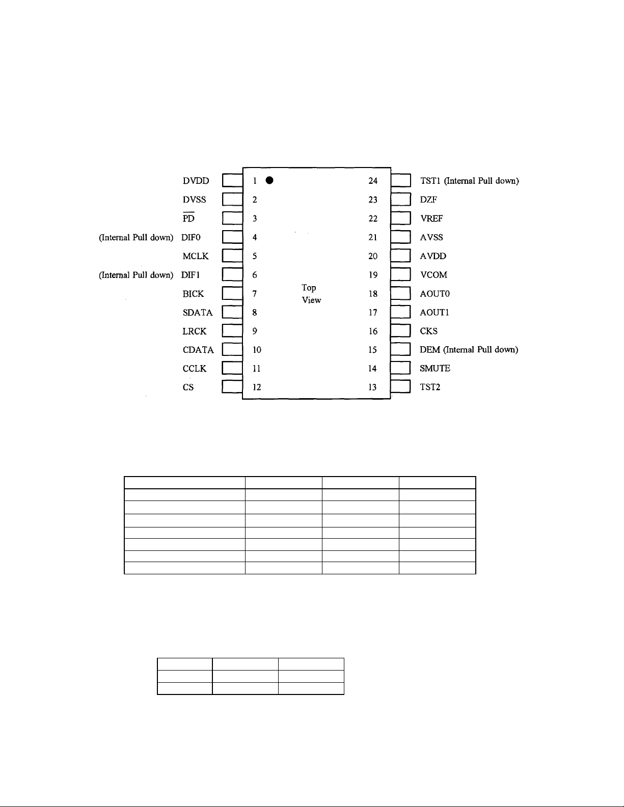
Pin Layout
Compatibility with AK4311/A
1. Changed Specs
Parameter AK4311 AK4311A AK4317
Resolution 16bit 16bit 16/18bit
Operating Temperature
Power Supply
Digital I/F level CMOS CMOS TTL
X'tal Oscillator Yes Yes No
DR 92dB 91dB 92dB
Package SSOP SSOP VSOP
-40∼85°C-10
3∼5.5V 3∼5.5V 4.5∼5.5V
C-40
∼70°
∼85°
C
2. Pin Compatibi lity
The following pin functions are changed fr om AK4311/A. But when X'tal oscillating circuit is not used, it
is possible to chan ge A K4311/A to AK4317 without changing the board layout.
Pin No. AK4311/A AK4317
4XTODIF0
6CLKODIF1
0172-E-01 1997/5
- 2 -
ASAHI KASEI [AK4317]
PIN/FUNCTION
No. Pin Name I/O Function
1 DVDD - Digital Power Supply
2 DVSS - Digital Ground Pin
3 PD I Power-Do wn Mode Pin
When at "L", the AK4317 is in p ower-down mode and is held in reset.
The AK4317 should always be reset upon po wer-up.
4 DIF0 I Digital Input Format Pin (Internal Pull-down pin)
5 MCLK I Master Clock Input Pin
6 DIF1 I Digital Input Format Pin (Internal Pull-down pin)
7 BICK I Audio S erial Data Clock Pin
8 SDATA I Audio Serial Data Input Pin
2's complement MSB-first data is input on t his pin.
9 LRCK I L/R Clock Pin
10 CDATA I Control Data Input Pi n
Must be tied to "H" or "L" if this pin is not used.
11 CCLK I Control Clock Pin
Must be tied to "H" or "L" if this pin is not used.
12 CS I Chip Select Pin
Must be tied to "H" if this pin is not used.
13 TST2 O Test Pin
Must be left floating.
14 SMUTE I Soft Mute Pin
When this pin goes "H", soft mute cycle is initiated.
When returning "L", the output mute releases.
15 DEM I De-emphasis Enable Pin (Internal Pull-dow n pin)
16 CKS I Master Clock Select Pin
MCLK=256fs,"H": MCLK=384fs
17 AOUT1 O Channel 1 analog output pin
18 AOUT0 O Channel 0 analog output pin
19 VCOM I Common Voltage Pin, AVDD/2
Normally connected to AVSS with a 0.1uF ceram ic capacitor in paralle l
with a 10uF electrolytic cap.
20 AVDD - Analog Power Supply Pin
21 AVSS - Analog Ground pin
22 VREF I Voltage Reference Input Pin
The differential Voltage between this pin and AVSS set the analog output
range. Normally connected t o AVSS with a 0.1uF cerami c capacitor .
23 DZF O Zero Input D etect Pin
24 TST1 I T est Pin
Must be left floating or tied to AVSS.
Note: All input pins except pull-down pins should not be lef t floating.
0172-E-01 1997/5
- 3 -
ASAHI KASEI [AK4317]
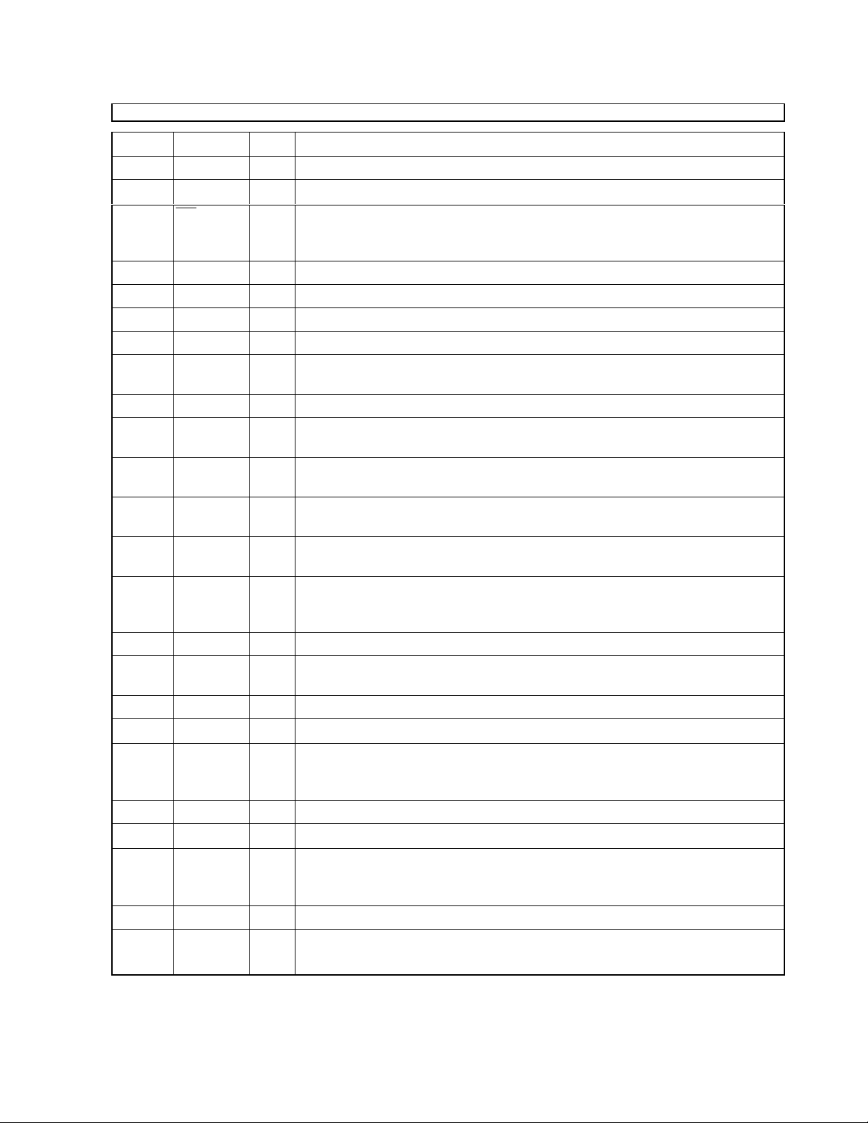
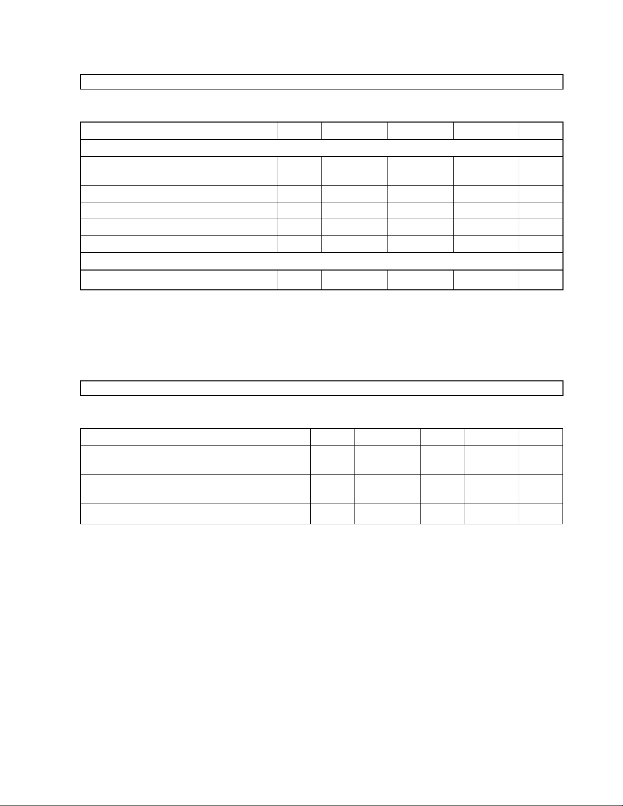
ABSOLUTE MAXIMUM RATINGS
(AVSS,DVSS=0V; Note 1 )
Parameter Symbol min max Units
Power Supplies: Analog
Digital
DADD-AVDD
AVDD
DVDD
VDA
-0.3
-0.3
Input Current, Any Pin Except Supplies IIN -
6.0
6.0
-
0.3
±
10
V
V
V
mA
Input Voltage VIND -0.3 A VDD+0.3 V
Ambient Operating Temperature Ta -40 85
Storage Temperature Tstg -65 150
C
°
C
°
Note: 1 . All voltages with respect to g r ound.
WA R NI NG: Operation at or be yond these limits may result in permanent damage to the devi ce.
Normal operation is not guaranteed at these extremes.
RECOMMENDED OPERATING CONDITIONS
(AVSS,DVSS=0V; Note 1 )
Parameter Symbol min typ max Units
Power Supplies: Analog (Note 2 )
Digital
AVDD
DVDD
4.5
4.5
5.0
5.0
5.5
AVDD
Voltage Reference (Note 3 ) VREF 2.5 - AVDD V
Notes: 2. AVDD and DVDD should be powered at the same t ime or AVDD should be powered earlier
than DVDD.
3. Analog output vo lt age scales with the voltage of VREF.
AOUT(typ.@0dB)=2.8Vpp*VREF/5.
* AKM assumes no responsibility for the usage beyond the conditions in t his data sheet.
V
V
0172-E-01 1997/5
- 4 -
ASAHI KASEI [AK4317]
ANALOG CHARACTERISTICS
(Ta=25°C; AVDD,DVDD=5.0V; VREF=AVDD; fs=44.1kHz; Signal Frequency=1kHz; 18bit Input Data;
Measurement Bandwidth=10Hz∼20kHz; R
10kΩ; unless otherwise specified)
L
≥
Par ameter min typ max Units
Resolution 18 Bits
Dynamic Characteristics (Note 4 )
THD+N (0dB Output) -80 -86 dB
Dynamic Range (-60dB Output, A weight) 88 92 dB
S/N (A weight) 88 92 dB
Interchannel Isolation(1kHz) 80 90 dB
DC Accuracy
Interchannel Gain Mismatch 0.15 0.3 dB
Gain Drift (Note 5 ) 20 -
ppm/°C
DC Accuracy
Output Voltage (Note 6 ) 2.66 2.8 2.94 Vpp
Load Resistance 10
k
Ω
Power Supplies
Power Sup ply Current
Normal Operation (PD="H")
AVDD
DVDD
12
4
18
6
mA
mA
Power- Down-Mode (PD="L")
AVDD+DVDD (Note 7 )
10
50
uA
Power Dissipation (AVDD+D VDD)
Normal Operation
Power-Down-Mode (Note 7 )
80
50
120 mW
uW
Power Supply Rejection (Note 8 ) 50 dB
Notes: 4. Measured by AD725 C(SHIBASOKU). Averaging mode. Refer to the eva board manual.
5. The voltage o n VREF pin is held +5V ext e rnally.
6. Full-scale vo lt age(0dB). Output voltage scales with the voltage of VREF pin.
AOUT(typ.@0dB)=2.8Vpp*VREF/5.
7. Power Dissipation in t he power-do wn mode is applied with no external clocks
(MCLK,BICK,LRCK held "H" or "L").
8. PSR is applied to AVDD,DVDD with 1kHz, 100mVpp . VREF pin is held +5V.
0172-E-01 1997/5
- 5 -
ASAHI KASEI [AK4317]
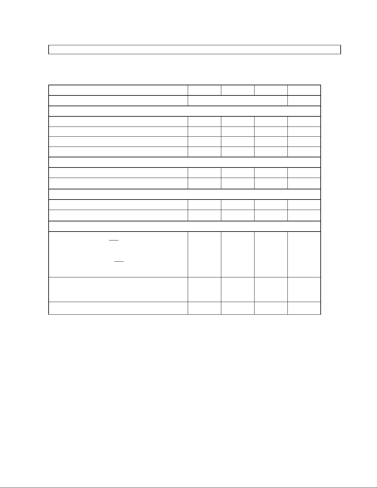
FILTER CHARA CTERISTICS
(Ta=25°C; AVDD,DVDD=4.5V∼5.5V; fs=44.1kHz; DE M="0")
Para meter Symbol min typ max Units
Digital Filter
Passband ±0.1dB (Note 9 )
-6.0dB
PB 0
- 22.05
20.0
-
kHz
kHz
Stopband (Note 9 ) SB 24.1 kHz
0.06
Passband Ripple PR
±
dB
Stopband Attenuation SA 43 dB
Group Delay (Note 10 ) G D - 14.7 - 1/fs
Digital Filter + SCF + CTF
0.5
Frequen cy Response 0∼20.0kHz
-
±
-dB
Note: 9. The passband and stopband frequencies scale with fs.
For examp le, P B=0.4535*fs(@±0.1dB), SB=0.546*fs.
10. The calc ulating delay t ime which occurred b y digital filtering. This time is from setting the
16/18bit data of both channels to input register to the output of anal og signal.
DIGITAL CHARACTERISTICS
(Ta=25°C; AVDD,DVDD=4.5∼5.5V)
Parameter Symbol min typ max Units
High-Level Input Voltage
Low-Le vel Input Voltage
High-Level Output Voltage (Iout=-100A)
Low-Le vel Output Voltage (Iout=100A)
VIH
VIL
VOH
VOL
2.2
-
DVDD-0.5
-
-
-
--
Input Leakage Current (Note 11 ) Iin - -
Notes: 11. DIF0,DIF1,DEM,TST1 pins have internal pull-do wn devices, nominally 160kΩ.
-
0.8
0.5
10 uA
±
V
V
V
V
0172-E-01 1997/5
- 6 -

ASAHI KASEI [AK4317]
SWITCHING CHARACTERISTICS
(Ta=25°C; AVDD,DVDD=4.5∼5.5V; CL=20pF)
Parameter Symbol min typ max Unit
Master Clock Timing 256fs:
Pulse Width Low
Pulse Width High
384fs:
Pulse Width Low
Pulse Width High
LRCK
Frequency
Duty Cycle
fCLK
tCLKL
tCLKH
fCLK
tCLKL
tCLKH
fs
Duty
2.048
28
28
3.072
23
23
8
45
12.8
19.2
44.1 50
55
MHz
ns
ns
MHz
ns
ns
kHz
kHz
%
Serial Interface Timing
BICK Period
BICK Pulse Width Low
Pulse Width High
BICK rising to LRCK edge (Note 12 )
LRCK Edge to BICK rising (Note 12 )
SDATA Hold Time
SDATA Setup Time
tBCK
tBCKL
tBCKH
tBLR
tLRB
tSDH
tSDS
312.5
100
100
50
50
50
50
ns
ns
ns
ns
ns
ns
ns
Control Interface Timing
CCLK Pulse Width Low
Pulse Width Hi gh
CDATA Latch Hold Time
CDATA Latch Setup Time
CS Pulse Wi dt h Low
CCLK to CS falling
CS rising to CCLK
tCCKL
tCCKH
tCDS
tCDH
tCSW
tCSS
tCSH
100
100
50
50
100
50
50
ns
ns
ns
ns
ns
ns
ns
Reset Timing
PD Pulse Wi dt h (Note 13 ) tPD 150 ns
Notes: 12. BICK rising edge must not occur at the same time as LRCK edge.
13. The AK4317 can be reset by bringi ng PD "L" to "H" only upon pow er up.
0172-E-01 1997/5
- 7 -

ASAHI KASEI [AK4317]
Timing Diagram
t
PD
PD
VIL
Reset Timing
0172-E-01 1997/5
- 8 -

ASAHI KASEI [AK4317]
OPERATION OVERVIEW
System Clock
The external clocks which are required to operate the AK4317 are MCLK, LRCK, BICK. The master
clock(MCLK)sho uld be synchronized w ith LRCK but the phase is not critical. The MCLK is used to
operate the digital int erpolation f i lter and the delta-sigma modul at or. The frequency of MCLK is
determined by the sampling rate (LRCK) and CKS pin. Table 1 illustrates corresponding clock
frequencies. When the 384fs is sele ct ed, the internal master clock beco mes 256fs(=384fs*2/3). Refer to
Figure 1 .
All external cloc ks(MCLK,BICK,LRCK) should always be present whenever the AK4317 is in normal
operation mode(PD=" H"). If these clocks are not provided, the AK4317 may draw excess current because
the device util izes dynamic refreshed lo gic internally. If the external clocks are not pr esent, the AK4317
should be in the power-do w n mo de(P D="L"). After exiting reset at po wer-up etc., the AK4317 is in powerdown mode until M CLK and LRCK are input.
Clock frequency
LRCK (fs)
8
k∼50kHz
BICK
64fs
∼
CKS="L" 256fs
MCLK
CKS="H" 384fs
Table 1 . System Cloc ks
Figure 1 . MCLK divider
Audio Serial Interface Format
Data is shifted in via the SDATA pin using BICK and LRCK inputs. Four serial dat a modes which are
compatible with A K4319 are supported and selected by t he DIF0 and DIF1 pins as shown in Table 2 . In
all modes the serial data is MS B-f irst, 2's compliment format and is latched on the rising edge of BICK.
Mode 2 can be used for 16 MSB justified formats by zeroing the u nused LSBs.
DIF1 DIF0 Mode BICK Figure
0 0 0: 16bit LSB Justified
32fs
≥
Figure 2
0 1 1: 18bit LSB Justified
1 0 2: 18bit MSB Justified
113: I2S Compatible
36fs
≥
36fs
≥
36fs
≥
Figure 2
Figure 3
Figure 4
or 32fs
Table 2 . Serial Data Modes
0172-E-01 1997/5
- 9 -

ASAHI KASEI [AK4317]
Figure 2 . Mode 0,1 Timing
Figure 3 . Mode 2 Timing
Figure 4 . Mode 3 Timing
De-emphasis filter
The AK4317 includes the digital de-emphasis filt er(t c=50/ 15us) by IIR filter. This filter correspo nds t o
three sampling frequencies(3 2kHz,44.1kHz,48kHz). De-emphasis is enabled by the following two ways.
1. DEM pin
Only one de-emphasis(fs=44.1kHz) set initially can be c ont rol led by DEM pin at resettin g. The deemphasis is enabled by setting DEM pin "H". When the frequency of de-emphasis is set by FS0,FS1 of
serial mode control bits, the corresponding de-emphasis can be enabled. In this case, DEM bit in the
serial mode control should be "0".
2. DEM bit in the serial mode control
DEM pin should be open or "L". In this case, The de-emphasis correspond ing to fs=32kHz,
44.1kHz,48kHz can be controlled by DEM, FS0 and FS1 in the serial mode control b its.
0172-E-01 1997/5
- 10 -

ASAHI KASEI [AK4317]
Zero detection
When the input data at both channels are continuousl y zeros for 81 92 LRCK cycles, DZF goes to "H".
DZF immediately go es "L" if input data are not zero after go ing DZF "H".
Soft mute operation
Soft mute operat ion is performed at digital domain. Whe n SMUTE pin goes "H" or the output mode is set
to "MUTE", the output signal is att enuated by -∞ during 1024 LRCK cycles. W hen SMUTE pin is returned
to "L" or exiting "MUTE", the mute is cancelle d and t he output attenuatio n gradually chan ges t o 0dB
during 1024 LRCK cycles. If the soft mute is cancelled within 1024 LRCK cycles after starting the
operation, the atten uation is discontinued and returned to 0dB. The soft mute is effective for changing the
signal source without stopp i ng the signal transmiss ion
Notes:
1
The output signal is att enuated by -∞ during 1024 LRCK cycles(1024/fs).
{
2
Analog output corresponding to digital input have the group delay(GD).
{
3
If the soft mute is cancelled within 1024 LRCK cycles, the attenuatio n is discontinued and
{
returned to 0dB.
4
As the input data at both channels are continuously z eros for 8192 LR C K cycles, DZF goes to
{
"H".
DZF immediately go to "L" if input data are not zero after DZ F "H".
Figure 5 . Soft mute and zero detection
0172-E-01 1997/5
- 11 -

ASAHI KASEI [AK4317]
Serial Mode Cont rol
The AK4317 can control out put at tenuation level, output mode, de-emphasis ty pe and attenuation mode
via the serial interface. The serial data consists of two 8 bits for setting the at t enuation level of each
channel and 8 bits for the mode control.
Figure 6 . Configur at ion of attenuator and mixer
L0-L7: Lch ATT data, L0=LSB, L7=MSB :FFH at RESET
R0-R7: Rch ATT data, R0=LSB, R7=MSB :FFH at RE SET
S0-S3: Output mode Control :1001 at RESET
DEM: De-Emphasis Control :0 at RESET
ATC: ATT mode Control :0 at RESET
FS0,FS1: fs Control for de-emphasis Filter :00 at RESET
Note 1: CCLK should be held "H" or "L" except writing to ATT & mode registers in order to avoid the
performance degradation.
Note 2: If the above serial mode control is not used, CS should be h el d "H".
Figure 7 . Serial mode control timing
1. Attenuator Operation
The AK4317 has individu ally controllable attenuator with linear scale and 256 levels f or each channel.
Equation of attenuation level: ATT=20×Log
(Binary level/ 255)
10
FFH: 0dB
:
01H: -48.1dB
00H: Mute(Infinity zero:-∞)
The transition between ATT values is same as soft mute operat i on. When current value is ATT1 and new
value is set as ATT2, ATT1 gradually becomes ATT2 with same operation as soft mute. If new value i s set
as ATT3 before reaching ATT2, ATT value gradually becomes ATT3 from the way of transition.
Cycle time of soft mute: Ts=1024/fs
When resetting, ATT value is set 00H(Infinity zero). ATT value gradually changes fr om 00H to FFH(0dB)
during Ts af t er exiting reset.
0172-E-01 1997/5
- 12 -

ASAHI KASEI [AK4317]
2. Output mode
The AK4317 supports the following output modes .
•
Normal stereo output
•
L/R Reverse output
•
Monaural output: L/L, R/R, (L+R)/2
•
Output muting with soft mute operation
When resetting, ATT values of both channels are FFH and t he attenuation levels are set 0dB. The output
mode is also set normal stereo output.
S0 S1 S2 S3 AOUT0 AOUT1 Mode
0000 MUTE MUTE MUTE
0001 MUTE R
0010 MUTE L
0011 MUTE (L+R)/2
0100 R MUTE
0101 R R
0110 R L Reverse
0111 R (L+R)/2
1000 L MUTE
1001 L R Stereo * at RESET
1010 L L
1011 L (L+R)/2
1100 (L+R)/2 MUTE
1101 (L+R)/2 R
1110 (L+R)/2 L
1111 (L+R)/2 (L+R)/2 MONO
Table 3 . Output mode
3. De-em phasis control
DEM bit and DEM pin are ORed internally. The de-emphasis(tc=50/15us) corresponding to fs(sampling
frequency)selected by FS0 and F S1 is ena bled by setting DEM b it "1" or DEM pin "H". When DEM bit is
"0" and DEM pin is "L", the de-emphasis is disabled and the sett ing of FS0 and FS1 is invalid. The deemphasis is also disabled at F S0="1" and FS1="0". When resetting, DEM bit is set "0". For example,
when the de-emphasis is cont rol led by only DEM pin at fs =44. 1kHz, DEM,FS0,FS1 bit s should be "0".
This condition is also set at resetting.
FS0 FS1 mode
0 0 44.1kHz
10 OFF
0 1 48kHz
1 1 32kHz
Table 4 .De-emphasis filt er set ting
(Valid at DEM bit="1" or DEM pin="H")
4. Attenuation control
ATT values of both channels are set Lch ATT data by setting ATC bit "1". In this case, Rch ATT data is
ignored. When resetting, ATC bit is set "0" (indivi dually control).
0172-E-01 1997/5
- 13 -

ASAHI KASEI [AK4317]
Power-Down
The AK4317 are placed in the p ower-down m ode by bringing PD pin "L" and the analog outputs are
floating(Hi-Z). Figure 8 shows an ex ample of the system timing at the power-down and power-up .
Figure 8 . P ower-down/ up sequence example
Notes:
1
Analog output corresponding to digital input have the group delay(GD).
{
2
Analog outputs are floating(Hi-Z) at the pow er-d own mode.
{
3
Click noise about -50dB occurs at the edges("↑↓") of PD signal.
{
This noise is output even if "0" data is i nput.
4
When the external clocks(MCLK,BICK,LRCK) are stopped, the AK4317 should be in the po wer-
{
down mode.
5
Please mute the analog output external ly if the click noise(
{
The timing example is shown in this fi gure.
System Reset
The AK4317 should be reset once by bringing PD "L" upon power-up. The AK4317 is powered up and
the internal timing starts clocking by LRCK "↑" after exiting reset and po wer down state by MCL K. The
AK4317 is in power-down mode until LRCK is in put.
Click Noise from analog output
Click noise occurs f r om analog output in the following case s.
1
When switch ing de-empahsis mode by DEM bit or DEM pin.
{
2
When switching serial data mode by DIF0,DIF1 pins,
{
3
When going and exiting power down mode by PD pin,
{
1
2
&
Howe ver in case of
from SMUTE="H"), no click noise occur.
{
, If the input data is "0" or the soft m ute is enabled (after 10 24 LRCK cycles
{
3
) influences system application.
{
0172-E-01 1997/5
- 14 -

ASAHI KASEI [AK4317]
SYSTEM DESIGN
Figure 9 shows the system connection diagr am. An evaluation board[AKD4317] is availa ble which
demonstrates the optimum layout, power su pply arrangements an d measurement results.
Figure 9 . Typical Connection Diagram
Notes:
- LRCK=fs, MCLK=256fs at CKS="L", MCLK=384fs at CKS="H".
- If the above serial mode control is not used, CS should be held "H".
- Power lines of AVDD and DVDD should be distributed separate ly fr om t he point with low
impedance of regulator etc.
- When AOUT drives some ca pacitive loa d, some resistor should be added in series bet ween
AOUT and capacitive lo ad.
- The capacitor value on VCOM depends on low frequency noise level of power supply.
- All input pins except pull-down pins(DIF0,DIF1,DEM,TST1) should not be left floating.
0172-E-01 1997/5
- 15 -

ASAHI KASEI [AK4317]
1. Groundin g and Power Supply D ecoupling
To minimize coupling by digital noise , decoupling capacitors should be connected to AVDD and DVDD,
respectively. AVDD is supplied from analog supply in system and DVDD is supplied from AVDD via 10
Ω
resistor as shown inFigure 9 . Alternatively if AVDD and DVDD are supplied separately, AVDD and DVDD
should be powered at the same time or AVDD should be powered earlier than DVDD. Analog ground and
digital ground sho uld be connected together near to where the supplies are brought onto the printed
circuit board. Decoupli ng capacitors for hi gh f r equency should be placed as near as possible.
2. Voltage reference
The differenti al Voltage between VREF and AVSS set the analog output range. VREF pin is normally
connected to AVDD with a 0.1uF ceramic capacitor. VCOM is a signal ground of this chip . An electrolytic
capacitor of around 10uF in parallel with a 0.1uF ceramic capacitor attached to these pins elimin at es t he
effects of high fr equency noise. No load current may be drawn from VCOM pin. All signals, especially
clocks, should be kept a way from the VREF and VCOM pins in order to avoid unwanted coupling into the
AK4317.
3. Analog Outputs
The analog outputs are also single-ended and centered arou nd t he VCOM voltage. The output s ign al
range is typically 2.8 Vpp. AC coupling capacitors of larg er than 1uF are recommended. The internal
switched-capacitor filter and contin uous-time filter attenuate the noise generated by the delta-sigma
modulator beyond the audio passband. Therefore, any external filters are not require d for typical
application. The output voltage is a posit ive full scale for 1FFFFH(@18bit ) and a negative fu ll scale for
20000H(@18bit). The ideal output is VCOM voltage for 00000H(@18bit).
DC offsets on analog outputs are eliminated by AC coupling since analog outputs have DC offsets of
VCOM + a few mV.
0172-E-01 1997/5
- 16 -

ASAHI KASEI [AK4317]
PACKAGE
zzzz
24pin VSOP (Unit: mm)
NOTE: Dimension “*” does not include mold flash.
Pac kage & Lead frame material
Package molding compound: Epoxy
Lead frame material: Cu
Lead frame surface treatme nt: Solder plate
0172-E-01 1997/5
- 17 -

ASAHI KASEI [AK4317]
MARKING
Contents of AAXXXX
AA: Lot#
XXXX: Date Code
0172-E-01 1997/5
- 18 -

IMPORTANT NOTICE
z These products and their specifications are subject to change without notice. Before
considering any use or application, consult the Asahi Kasei Microsystems Co., Ltd. (AKM)
sales office or authorized distributor concerning their current status.
z AKM assumes no liability for infringement of any patent, intellectual property, or other
right in the application or use of any information contained herein.
z Any export of these products, or devices or systems containing them, may require an
export license or other official approval under the l aw and regulations o f the country of
export pertaining to customs and tariffs, currency exchange, or strategic materials.
z AKM products are neither intended nor authoriz ed for use as c ritical components in any
safety, life support, or other hazard related device or system, and AKM assumes no
responsibility relating to any such use, except with the express written consent of the
Representative Director of AKM. As used here:
(a) A hazard related device or system is one designed or intended for life support or
maintenance of safety or for applications in medicine, aerospace, nuclear ener gy, or
other fields, in which its failure to function or perf orm may reasonably be expected to
result in loss of life or in significant injury or damage to person or property.
(b) A critical com ponent is one whose failure to fu nction or perform may reasonably be
expected to result, whether directly or indirectly, in the loss of the safety or
effectiveness of the device or system containing it, and which must therefore meet
very high standards of performance and reliability.
z It is the responsibility of the buyer or distributor of an AKM product who distributes,
disposes of, or otherwise places the product with a third party to notify that party in
advance of the above content and conditions, and the buyer or distributor agrees to
assume any and all r esponsibility and liability for and ho ld AKM harmless from any and
all claims arising from the use of said product in the absence of such notification.
 Loading...