

Page 1
[ASAHI KASEI]
[AK4170]
AK4170
Features
n Ultra smooth output waveform
n Support full speed(12Mbps) and low speed(1.5Mbps)
n Single Power Supply 3.3 volts ± 10%
n 16pin TSSOP package
n Functionally compatible to Philips PDIUSBP11
n Support suspend mode
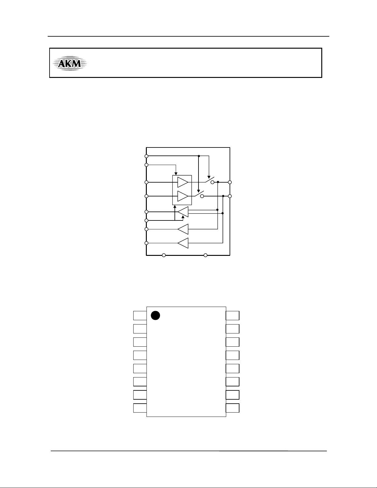
OEN
FAST
INP
INN
RDIFF
SUS
RSHP
RSHN
USB Transceiver
DP
DN
+
-
nPin Layout
OEN
RDIFF
RSHP
RSHN
SUS
VSS
NC
VSSVDD
AK4170 Block Diagram
1NC
2
3
4
5
6
7
8
16 VDD
15
INN
14
INP
13
DP
12
DN
11
FAST
10
NC
NC
9
<M0066-E-01> <1999/09>
- 1 -
Page 2
[ASAHI KASEI]
Pin/Function
No. Signal Name I/O Description
1 NC - Not Connected
2 OEN I Output Enable Pin (CMOS level digital input)
Low input enables transmit data, it is that both INP and INN output onto DP and
DN pins. High input enable receive mode, which disables the outputs of DP and
DN, and the buffer goes into high-z state.
3 RDIFF O Differential Receiver Output (CMOS level digital output)
When DP > DN, the output is H. When DP < DN, the output is L.
When both DP and DN are L, the output is not guaranteed.
this pin also outputs correctly regardless of the OEN input.
4 RSHP O Schmitt Hysteresis Receiver Output for DP (D+) input (CMOS level digital output)
When DP is high level, RSHP is high.
When DP is low level, RSHP is low
this pin also outputs correctly regardless of the OEN input.
5 RSHN O Schmitt Hysteresis Receiver Output for DN (D-) input (CMOS level digital output)
When DN is high level, RSHN is high.
When DN is low level, RSHN is low
this pin also outputs correctly regardless of the OEN input.
6 SUS I Suspend Mode Control Pin (CMOS level)
High input forces the RDIFF output to low level, and the AK4170 goes into low
power consumption mode regardless of OEN pin.
7 VSS P Ground Pin
8 NC - Not Connected
9 NC - Not Connected
10 NC - Not Connected
11 FAST I Full Speed/Low Speed Control Input (CMOS digital input)
Low input activates the AK4170 to Low Speed (1.5Mbps) mode.
High input activates the AK4170 to Full Speed (12Mbps) mode.
12 DN I/O Transmitter/Receiver Negative Data Output/Input Pin
DN outputs the data of INN logic level when OEN is low
DN disable the output, and goes to high-z state when OEN is high.
13 DP I/O Transmitter/Receiver Positive Data Output/Input Pin
DP outputs the data of INP logic level when OEN is low
DP disable the output, and goes to high-z state when OEN is high.
14 INP I Transmitter Positive Data Input Pin (CMOS digital input)
When OEN is low, DP outputs INP logic level.
When OEN is high, INP does not influence output pins.
15 INN I Transmitter Negative Data Input Pin (CMOS digital input)
When OEN is low, DN outputs INN logic level.
When OEN is high, INN does not influence output pins.
16 VDD - Power Supply Pin
Connected to VSS with a 0.1uF capacitor.
[AK4170]
<M0066-E-01> <1999/09>
- 2 -
Page 3
[ASAHI KASEI]
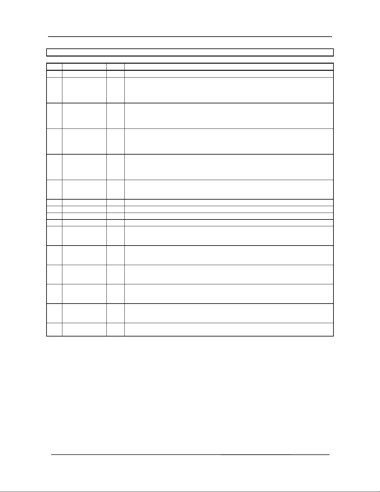
Absolute Maximum Rating
VSS=0V
Parameter Symbol min max Units
Power Supplies
VDD 4.5 V
Digital Input Voltage VIN VSS-0.3 VDD+0.3 V
Digital Output Voltage VO VSS-0.3 VDD+0.3 V
Ambient Temperature Ta -40 +125
Note 1. All voltages with respect to ground
Warning: Operation at or beyond these limits may results in permanent damage to the device. Normal operation is
not guaranteed at these extremes.
Recommended Operating Condition
VSS=0V
Parameter Symbol min typ max Units
Power Supplies
Operating Temperature
All voltages with respect to ground.
VDD 3.0 3.3 3.6 V
Ta 0 70
[AK4170]
°C
°C
<M0066-E-01> <1999/09>
- 3 -
Page 4

[ASAHI KASEI]
[AK4170]
Digital DC Characteristics
Ta=25°C; VDD=3.0 - 3.6V; VSS=0V Measurement under static state
Parameter Symbol min typ max Units
H level input voltage VIH 70%VDD V
L level input voltage VIL 30%VDD V
H level output voltage IOH=-1.5mA VOH 2.4 V
L level output voltage IOL= 3.0mA VOL - 0.6 V
H level Input Current VIH=VDD IIH 10
L level Input Current VIL=0V IIL 10 -
µA
µA
Transmitter Characteristics
Ta=25°C; VDD=3.0 - 3.6V; VSS=0V
Parameter Symbol Pins Conditions min typ max Units
Output Impedance(Hi) Roh DP, DN DP, DN=H 40
Ω
Output Impedance (Lo) Rol DP, DN DP, DN=L 40
H level Output Voltage Vohd DP, DN IOH=-200uA 2.8 V
L level Output Voltage Vold DP, DN IOH=2.2mA 0.3 V
Tri-state Leakage Current Iolk DP, DN OEN=H
-10 10
µA
0 < DP, DN< 3.3V
Low Speed Propagation Delay
(INP/INN to DP, DN)
Tpds DP, DN,
INP,
FAST=L 170 300 ns
INN
Full Speed Propagation Delay
(INP/INN to DP, DN)
Tpdf DP, DN,
INP,
FAST=H 15 20 ns
INN
Low Speed Rise/Fall Time
*)
Trs/Tfs DP, DN FAST=L 75 180 300 ns
Full Speed Rise/Fall Time**) Trf/Tff DP, DN FAST=H 4 12 20 ns
Rise/Fall Time Matching Trfm DP, DN FAST=L 100 %
Rise/Fall Time Matching Trfm DP, DN FAST=H 100 %
Crossover Point Vcrs DP, DN 1.6 V
OEN Mode Change Delay Tomcd DP, DN from OEN 10 ns
SUS Mode Change Delay Tsmcd DP, DN from SUS 10 ns
*) CL=50pF for min, CL=350pF max
=50pF
**) C
L
INP, INN
DP, DN
T
pdf
T
pds
T
pdf
T
pds
V
=0.5xVDD
M
VM=0.5xVDD
DP, DN
T
T
rs
rf
T
T
fs
ff
90%VDD
10%VDD
Ω
Figure Rise/Fall Time
Figure Propagation Delay
DP, DN
Vcrs
Figure Crossover Point
<M0066-E-01> <1999/09>
- 4 -
Page 5

[ASAHI KASEI]
[AK4170]
T
omcd
V
=0.5xVDD
M
VM=0.5xVDD
OEN
DP, DN
T
omcd
Figure OEN Mode Change Delay
Receiver Characteristics
Ta=25°C; VDD=3.0 3.6V; VSS=0V
Parameter Symbol Pins Conditions min typ max Units
Common Mode Range(CMR) CMR DP, DN 0.8 2.5 V
Differential Input Sensitivity DIS DP, DN within CMR 200 mV
Differential Receiver Delay Tdrd DP/DN to
RDIFF
Schmitt Buffer Delay Tsbd DP/DN to
RSHP,
CL@RDIFF
=50pF
CL@RSHP,
RSHN=50pF
14 25 ns
715ns
RSHN
Schmitt High Level Voltage Vihs DP, DN 2.0 V
Schmitt Low Level Voltage Vils DP,DN 0.8 V
<M0066-E-01> <1999/09>
- 5 -
Page 6

[ASAHI KASEI]
[AK4170]
|DP-DN|
Voltage Difference (V)
Figure Differential Input Sensitivity
DN
DP
RDIFF
Figure Differential Receiver Delay
1.0
0.2
0.0
0.0 3.32.52.31.00.8
T
drd
CMR
T
drd
V
=0.5xVDD
M
VM=0.5xVDD
DIS
DP,DN
RSHP
RSHN
DP, DN
T
sbd
T
sbd
Figure Schmitt Buffer Delay
Figure Schmitt Level Voltage
V
=0.5xVDD
M
VM=0.5xVDD
Vihs
Vils
<M0066-E-01> <1999/09>
- 6 -
Page 7

[ASAHI KASEI]
[AK4170]
Power Dissipation
Ta=25°C; VDD=3.0 - 3.6V ; VSS=0V
Parameter Symbol Conditions min typ max Units
Operational Current
(FAST=H,OEN=L)
Operational Current
(FAST=L,OEN=L)
Quiescent Current 1 Iddq1 Inputs idle state
Iddf 6MHz toggle input to
INP,INN
Idds 750KHz toggle input to
INP,INN
16 30 mA
915mA
5 10.0 mA
OEN=L, SUS=L
Quiescent Current 2 Iddq2 Input Idle State
450 900
µA
OEN=H, SUS=L
Suspend Current Iddsus Inputs idle state
4.0 80
µA
SUS=H
VDD
R2 on D+ only when FAST=H
R2=1.5k
R2 on D- only when FAST=L
DP, DN
R1=15k
DP, DN are the AK4170 side, while D+,D- are the USB bus
50pF (FAST=H)
50pF or 350pF (FAST=L)
D+,D-
<M0066-E-01> <1999/09>
- 7 -
Page 8

[ASAHI KASEI]
A
)
16pin TSSOP (Unit: mm
5.00TYP 1.10 MAX
[AK4170]
Package
916
0.22±0.08 0.65
| 0.13|M
Seating Plane
4.4TYP
18
1.10 MAX
Detail A
| 0.10
0.17±0.05
0.07±0.04
0-10
6.4
±
0.2
0.5
±
0.2
°
<M0066-E-01> <1999/09>
- 8 -
Page 9

[ASAHI KASEI]
[AK4170]
Marking
AKM
4170VT
XXYYY
Contents of XXYYY
XX: Lot #
YYY: Date Code
<M0066-E-01> <1999/09>
- 9 -
Page 10

[ASAHI KASEI]
[AK4170]
IMPORTANT NOTICE
These products and their specifications are subject to change without notice. Before considering any use or application,
consult the Asahi Kasei Microsystems Co., Ltd. (AKM) sales office or authorized distributor concerning their current status.
AKM assumes no liability for infringement of any patent, intellectual property, or other right in the application or use of any
information contained herein.
Any export of these products, or devices or systems containing them, may require an export license or other official approval
under the law and regulations of the country of export pertaining to customs and tariffs, currency exchange, or strategic
materials.
AKM products are neither intended nor authorized for use as critical components in any safety, life support, or other hazard
related device or system, and AKM assumes no responsibility relating to any such use, except with the express written
consent of the Representative Director of AKM. As used here:
A hazard related device or system is one designed or intended for life support or maintenance of safety or for applications
in medicine, aerospace, nuclear energy, or other fields, in which its failure to function or perform may reasonably be
expected to result in loss of life or in significant injury or damage to person or property.
A critical component is one whose failure to function or perform may reasonably be expected to result, whether directly or
indirectly, in the loss of the safety or effectiveness of the device or system containing it, and which must therefore meet very
high standards of performance and reliability.
It is the responsibility of the buyer or distributor of an AKM product who distributes, disposes of, or otherwise places the
product with a third party to notify that party in advance of the above content and conditions, and the buyer or distributor
agrees to assume any and all responsibility and liability for and hold AKM harmless from any and all claims arising from the
use of said product in the absence of such notification.
<M0066-E-01> <1999/09>
- 10 -
 Loading...