

Page 1
ASAHI KASEI [AK2546]
MCLK
AS(ALE)
RCLK1
RPOS
RNEG1
LOS1
DS(RD)
TEST1-5
TNEG1
TPOS
TCLK1
AD7-AD0
RESET
R /W (WR)
CS
BTS
INT
CLKSEL
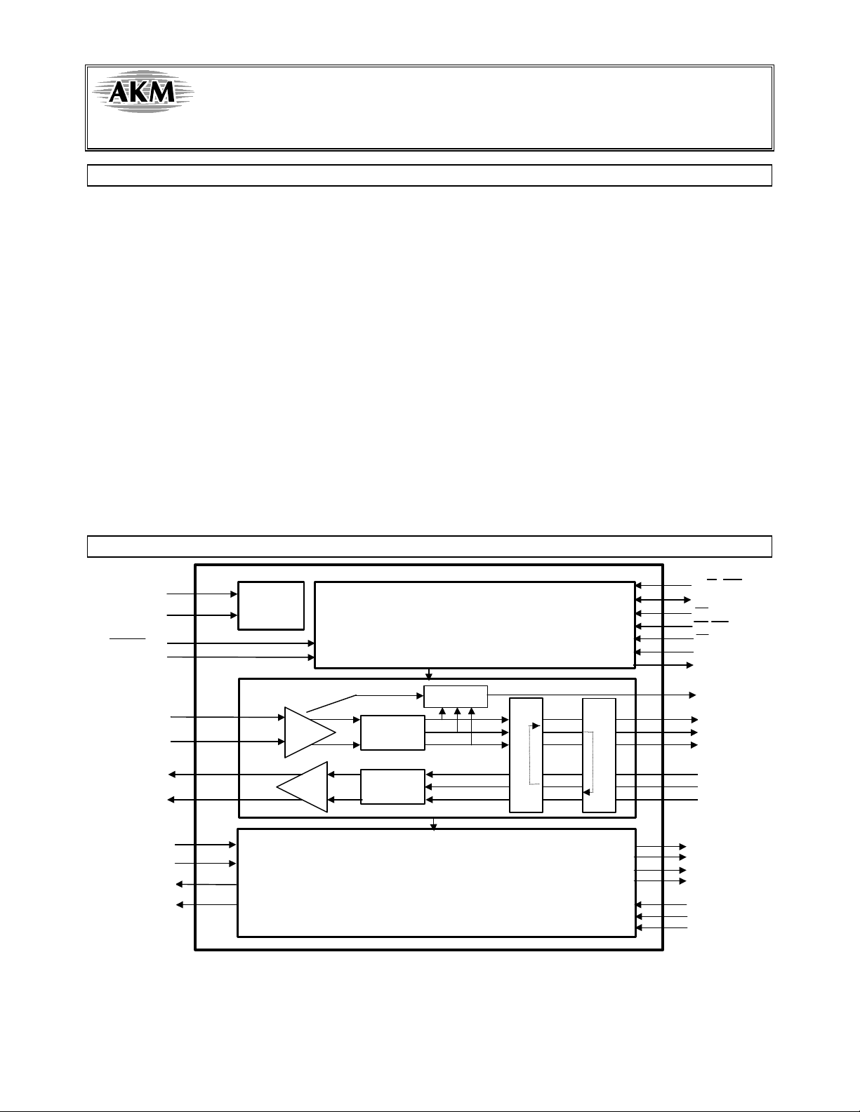
7 channel T1 Transceiver
FEATURE
• 7ch short haul T1 transceiver
• Jitter Tolerance: Compliant with GR-499 Category I, II
• Transmitter Pulse Shape: Compliant with GR-499
• Loss of Signal Detection
• Selectable Signal Polarity
• Local/Remote Loopback
• Parallel Microprocessor Interface
• Single 3.3V±5% Operation
• Low Power Consumption (105mW/ch: Typ)
• Pin-to-pin compatible with AK2548 (7 channel E1 transceiver)
• Small Plastic Package 144pin LQFP
AK2546
RTIP1
RRING1
TTIP1
TRING1
RTIP2-7
RRING2-7
TTIP2-7
TRING2-7
CLKGEN
TRANSCEIVER 1
TRANSCEIVER 2-7
BLOCK DIAGRAM
CONTROL
LOS
RECOVER
SHAPER
Local Loopback
Remote Loopback
LOS2-7
RCLK2-7
RPOS2-7
RNEG2-7
TCLK2-7
TPOS2-7
TNEG2-7
7 Channel T1 Transceiver Block Diagram
Page 2
ASAHI KASEI [AK2546]
73
144
143
142
141
140
139
138
137
136
135
134
133
132
131
130
129
128
127
126
125
124
123
122
121
120
119
118
117
116
115
114
113
112
111
110
109
36
72
AD7
RRING7
BTS
RRING6
TEST5
RRING5
TEST4
TEST3
RRING4
TEST2
RRING3
RRING2
TEST1
RRING1
GENERAL DESCRIPTION
The AK2546 is the 7 channel short haul T1 transceiver for a SONET MUX, M13 MUX, etc.
It includes seven independent transmitters, clock and data recovery, LOS detector, control circuit
in one LQFP-144 package which saves space, power consumption and the board design time.
Internally generated transmit pulse provides the appropriate pulse shape for line length ranging
from 0 to 655 feet from a DSX-1 cross connect.
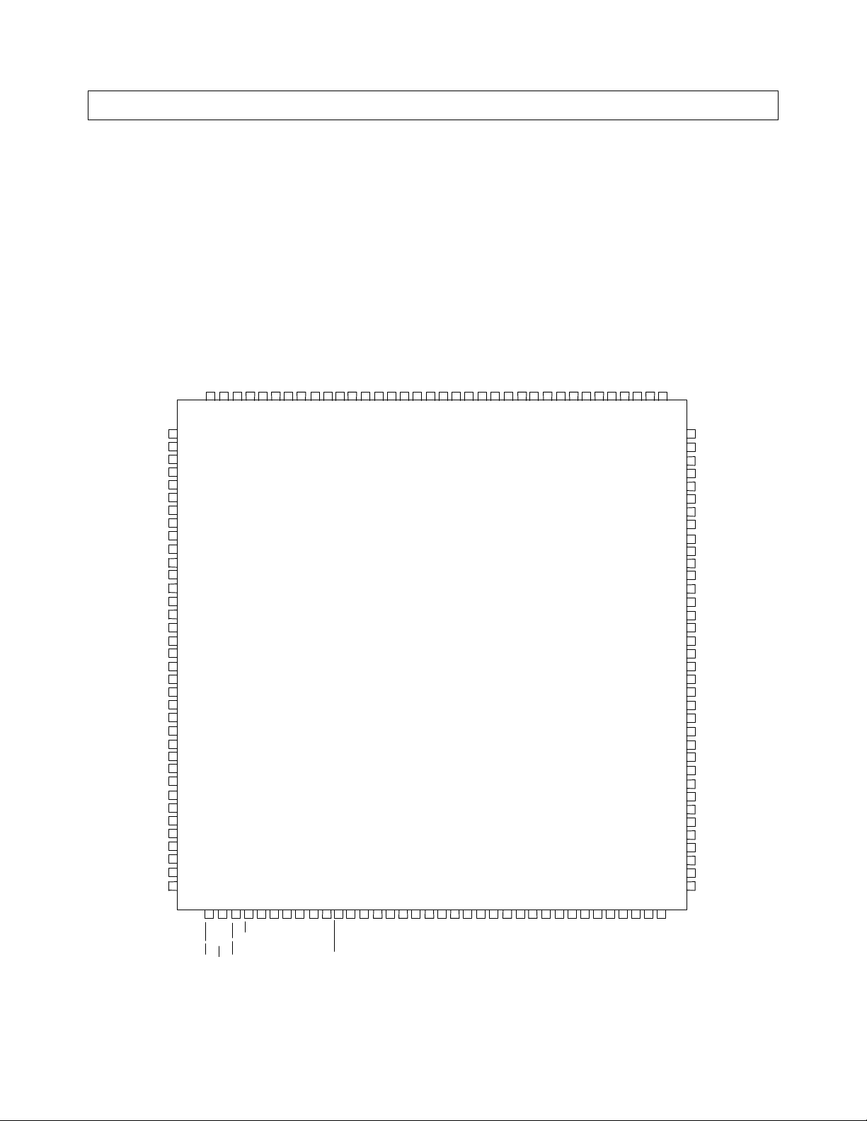
PIN ASSIGNMENTS
AVSS8
TTIP7
TVSS7
TVDD7
TRING7
AVSS7
TTIP6
TVSS6
TVDD6
TRING6
AVSS6
TTIP5
TVSS5
TVDD5
TRING5
AVSS5
TTIP4
TVSS4
TVDD4
TRING4
AVSS4
TTIP3
TVSS3
TVDD3
TRING3
AVSS3
TTIP2
TVSS2
TVDD2
TRING2
AVSS2
TTIP1
TVSS1
TVDD1
TRING1
AVSS1
TCLK7
TPOS7
TNEG7
RCLK7
RPOS7
RNEG7
TCLK6
TPOS6
TNEG6
RCLK6
RPOS6
RNEG6
IOVDD2
IOVSS2
TAVDD2
TAVSS2
TCLK5
TPOS5
TNEG5
RCLK5
RPOS5
RNEG5
DAVSS2
DVSS2
DVDD2
LOS7
LOS6
LOS5
AD0
AD1
AD2
AD3
AD4
AD5
AD6
1
2
3
4
5
6
7
8
9
10
11
12
13
14
15
16
17
18
19
20
21
22
23
24
25
26
27
28
29
30
31
32
33
34
35
3738394041424344454647484950515253545556575859606162636465666768697071
(TOP VIEW)
108
107
106
105
104
103
102
101
100
TCLK1
TPOS1
TNEG1
RCLK1
RPOS1
RNEG1
TCLK2
TPOS2
TNEG2
RCLK2
99
RPOS2
98
RNEG2
97
IOVDD1
96
IOVSS1
95
TAVDD1
94
TAVSS1
93
TCLK3
92
TPOS3
91
TNEG3
90
RCLK3
89
RPOS3
88
RNEG3
87
DAVSS1
86
DVSS1
85
DVDD1
84
TCLK4
83
TPOS4
82
TNEG4
81
RCLK4
80
RPOS4
79
RNEG4
78
LOS1
77
LOS2
76
LOS3
75
LOS4
74
RAVDD1
CS
INT
PVSS
MCLK
AS(ALE)
R/W(WR)
RAVSS2
PVDD
DS(RD)
RESET
RAVDD2
RTIP7
RTIP6
RTIP5
BVSS
BGREF
BVDD
RTIP4
RTIP3
CLKSEL
RTIP2
RTIP1
RAVSS1
Page 3
ASAHI KASEI [AK2546]
PIN CONDITION
Pin No. Pin Name I/O Pin Type AC Load DC Load Comments
1
2
3
4
5
6
7
8
9
10
11
12
13
14
15
16
17
18
19
20
21
22
23
24
25
26
27
28
29
30
31
32
33
34
35
36
TCLK7 I CMOS
TPOS7 I CMOS
TNEG7 I CMOS
RCLK7 O CMOS ≤15pF
RPOS7 O CMOS ≤15pF
RNEG7 O CMOS ≤15pF
TCLK6 I CMOS
TPOS6 I CMOS
TNEG6 I CMOS
RCLK6 O CMOS ≤15pF
RPOS6 O CMOS ≤15pF
RNEG6 O CMOS ≤15pF
IOVDD2 I Power
IOVSS2 I Power
TAVDD2 I Power
TAVSS2 I Power
TCLK5 I CMOS
TPOS5 I CMOS
TNEG5 I CMOS
RCLK5 O CMOS ≤15pF
RPOS5 O CMOS ≤15pF
RNEG5 O CMOS ≤15pF
DAVSS2 I Power
DVSS2 I Power
DVDD2 I Power
LOS7 O CMOS ≤15pF
LOS6 O CMOS ≤15pF
LOS5 O CMOS ≤15pF
AD0 I/O CMOS ≤50pF
AD1 I/O CMOS ≤50pF
AD2 I/O CMOS ≤50pF
AD3 I/O CMOS ≤50pF
AD4 I/O CMOS ≤50pF
AD5 I/O CMOS ≤50pF
AD6 I/O CMOS ≤50pF
AD7 I/O CMOS ≤50pF
Page 4
ASAHI KASEI [AK2546]
Pin No. Pin Name I/O Pin Type AC Load DC Load Comments
37
38
39
40
41
42
43
44
45
46
47
48
49
50
51
52
53
54
55
56
57
58
59
60
61
62
63
64
65
66
67
68
69
70
71
72
R/W(WR) I CMOS
AS(ALE) I CMOS
DS(RD) I CMOS
CS I CMOS
INT O Open drain PMOS
Open drain
PVDD I Power
MCLK I CMOS
PVSS I Power
RAVSS2 I Power
RAVDD2 I Power
RESET I CMOS
RRING7 I Analog
RTIP7 I Analog
BTS I CMOS
RRING6 I Analog
RTIP6 I Analog
TEST5 I CMOS Note1)
RRING5 I Analog
RTIP5 I Analog
TEST4 I CMOS Note1)
BVSS I Power
BGREF O Analog 12kΩ ±1% accuracy
BVDD I Power
TEST3 I CMOS Note1)
RRING4 I Analog
RTIP4 I Analog
TEST2 I CMOS Note2)
RRING3 I Analog
RTIP3 I Analog
CLKSEL I CMOS
RRING2 I Analog
RTIP2 I Analog
TEST1 I CMOS Note1)
RRING1 I Analog
RTIP1 I Analog
RAVSS1 I Power
Page 5
ASAHI KASEI [AK2546]
Pin No. Pin Name I/O Pin Type AC Load DC Load Comments
73
74
75
76
77
78
79
80
81
82
83
84
85
86
87
88
89
90
91
92
93
94
95
96
97
98
99
100
101
102
103
104
105
106
107
108
RAVDD1 I Power
LOS4 O CMOS ≤15pF
LOS3 O CMOS ≤15pF
LOS2 O CMOS ≤15pF
LOS1 O CMOS ≤15pF
RNEG4 O CMOS ≤15pF
RPOS4 O CMOS ≤15pF
RCLK4 O CMOS ≤15pF
TNEG4 I CMOS
TPOS4 I CMOS
TCLK4 I CMOS
DVDD1 I Power
DVSS1 I Power
DAVSS1 I Power
RNEG3 O CMOS ≤15pF
RPOS3 O CMOS ≤15pF
RCLK3 O CMOS ≤15pF
TNEG3 I CMOS
TPOS3 I CMOS
TCLK3 I CMOS
TAVSS1 I Power
TAVDD1 I Power
IOVSS1 I Power
IOVDD1 I Power
RNEG2 O CMOS ≤15pF
RPOS2 O CMOS ≤15pF
RCLK2 O CMOS ≤15pF
TNEG2 I CMOS
TPOS2 I CMOS
TCLK2 I CMOS
RNEG1 O CMOS ≤15pF
RPOS1 O CMOS ≤15pF
RCLK1 O CMOS ≤15pF
TNEG1 I CMOS
TPOS1 I CMOS
TCLK1 I CMOS
Page 6

ASAHI KASEI [AK2546]
Pin No. Pin Name I/O Pin Type AC Load DC Load Comments
109
110
111
112
113
114
115
116
117
118
119
120
121
122
123
124
125
126
127
128
129
130
131
132
133
134
135
136
137
138
139
140
141
142
143
144
AVSS1 I Power
TRING1 O Analog driver output
TVDD1 I Power
TVSS1 I Power
TTIP1 O Analog driver output
AVSS2 I Power
TRING2 O Analog driver output
TVDD2 I Power
TVSS2 I Power
TTIP2 O Analog driver output
AVSS3 I Power
TRING3 O Analog driver output
TVDD3 I Power
TVSS3 I Power
TTIP3 O Analog driver output
AVSS4 I Power
TRING4 O Analog driver output
TVDD4 I Power
TVSS4 I Power
TTIP4 O Analog driver output
AVSS5 I Power
TRING5 O Analog driver output
TVDD5 I Power
TVSS5 I Power
TTIP5 O Analog driver output
AVSS6 I Power
TRING6 O Analog driver output
TVDD6 I Power
TVSS6 I Power
TTIP6 O Analog driver output
AVSS7 I Power
TRING7 O Analog driver output
TVDD7 I Power
TVSS7 I Power
TTIP7 O Analog driver output
AVSS8 I Power
Note1 ) Should be connected to VSS externally.
Note2 ) Should be connected to VDD externally
Page 7
ASAHI KASEI [AK2546]
PIN DESCRIPTIONS
Pin Name I/O Function Comment
T1 Transceiver
TTIP1-7
TRING1-7
TPOS1-7
TNEG1-7
TCLK1-7 I Transmit Clock Input
RTIP1-7
RRING1-7
RPOS1-7
RNEG1-7
RCLK1-7 O Receive Clock Output recovered from receive data input
LOS1-7 O Loss of signal output
TVDD1-7 Positive Power Supply for the Transmit Driver
TVSS1-7 Negative Power Supply for the Transmit Driver
AVSS1-8 Analog ground
Common Block
MCLK I 1.544MHz or 24.704MHz External Reference Clock Input
AS(ALE) I Address Select(Address Latch Enable) Input
INT O Interrupt Output(PMOS open drain , should be tied to GND through
DS(RD) I Data Strobe(Read Enable) Input
R/W (WR) I Read/Write(Write Enable) Input
CS I Chip Select Input
BTS I Bus Type Select Input
AD0-AD7 I/O Address/Data Input/Output
CLKSEL I MCLK Select Input
RESET I Reset Input
OOTransmit Tip/Ring Output
Bipolar output over transmit transformer
IITransmit Positive/Negative Data Input
Input on the falling edge of TCLK
IIReceive Tip/Ring Input
Bipolar Input over receive transformer
OOReceive Positive/Negative Data Output
Output on the falling edge of RCLK
Output “high” when detect loss of signal
LOSx output is not masked by MLOSx register.
a resistor), Active High, INT output goes “high” when the alarm is
reported to any one of LOSx, LOTCx or LOMC registers. This pin can
be masked by MLOSx, MLOTCx or MLOMC registers.
BTS=“H” : Motorola Mode
BTS=“L” : Intel Mode
Used for read/write internal registers.
CLKSEL=“H”:1.544MHz
CLKSEL=“L”:24.704MHz
Active “Low” input pulse over 200ns initializes the internal circuit
and forces RPOSx/RNEGx output “low” and LOSx output “high”.
Page 8

ASAHI KASEI [AK2546]
Pin Name I/O Function Comment
Common block
TEST1,3-5 I Factory Use. Should be connected to VSS externally.
TEST2 I Factory Use. Should be connected to VDD externally.
TAVDD1,2 Positive Power Supply for the analog circuitry in the transmitters
TAVSS1,2 Negative Power Supply for the analog circuitry in the transmitters
RAVDD1,2 Positive Power Supply for the digital circuitry in the transmitters
RAVSS1,2 Negative Power Supply for the digital circuitry in the transmitters
DVDD1,2 Positive Power Supply for Digital
DVSS1,2 Negative Power Supply for Digital
DAVSS1,2 Ground for Digital
IOVDD1,2 Positive Power Supply for I/O
IOVSS1,2 Negative Power Supply for I/O
BVDD Positive Power Supply for Reference Circuit
BVSS Negative Power Supply for Reference Circuit
PVDD Positive Power Supply for PLL
PVSS Negative Power Supply for PLL
BGREF Bandgap Reference Output.
12k±1% external register should be connected across this pin and
VSS.
Page 9

ASAHI KASEI [AK2546]
ABSOLUTE MAXIMUM RATINGS
Parameter Symbol Min Typ Max Units Condition
DC Supply VDD -0.3 6.5 V
Input Voltage
Input Current IIN 10 mA
Storage Temperature Tstg -55 130 °C
Note) All voltages with respect to ground. :
All negative voltage pins = 0V. VDD apply to all positive voltage pins.
VIN1 -0.3 VDD+0.3 V Apply to except for RTIPx,
RRINGx
VIN2 -3 VDD+0.3 V Apply to RTIPx, RRINGx
RECOMMENDED OPERATING CONDITIONS
Parameter Symbol min typ max Units Condition
DC Supply VDD 3.135 3.3 3.465 V 3.3V±5%
Ambient Operating Temperature Ta -40 25 +85 °C
Note) All voltages with respect to ground. :
All negative voltage pins = 0V. VDD apply to all positive voltage pins.
ELECTORICAL CHARACTERISTICS
DC CHARACTERISTICS
Parameter Symbol min typ max Units Condition
Power Consumption(/ch) PD 105 260 mW Note1
Digital High-Level Output Voltage VOH 0.9VDD V IOH=-40µA
Digital Low-Level Output Voltage VOL 0.4 V IOL=500µA
Digital High-Level Input Voltage VIH 0.7VDD V
Digital Low-Level Input Voltage VIL 0.3VDD V
Input Leak Current Ii 10 µA
Output Current IOL 1.0 mA INT pin
Note1: typ : 50% mark, Room temp., VDD 3.3V, line length 399feet, Load 100Ω
max: 100% mark, Temp./VDD in all range, line length 655feet, Load 100Ω
Not include any other load (ex. External pull up register) except lines.
Page 10
ASAHI KASEI [AK2546]
RECEIVER
Receiver characteristics are guaranteed on the conditions as shown below.
VDD=3.3V±5%, VSS, GND=0V, Ta=-40~85°C,
MCLK frequency: 1.544MHz±100ppm, 24.704MHz±100ppm,
Bipolar input frequency: 1.544MHz±130ppm(reference input level: 3V0p±20%)
Parameter Symbol Min Typ Max Units Condition
Sensitivity -6 dB Note1
Loss of Signal Threshold 0.35 0.5 0.7 V Note2
Allowable Consecutive Zero before LOS 170 175 180 bits
S/X tolerance 12 dB Note3
Generated Jitter 30 nspp Note4
Low pulse density immunity
Jitter Tolerance
Note1: Relative value to the reference level. Compare at 772kHz with All Mark Pattern.
Note2: Level at the chip side of transformer. Loss of signal is logical AND between an analog loss of
Signal monitors input level and a digital loss of signal check recovered data stream.
Note3: PN20 and AMI 1/8 Mark pattern input. Noise frequency is 770kHz.
Note4: PN20 pattern input.
GR-499 Category I,II
1/16 Mark
JITTER TOLERANCE
100
10
1
0.1
Jitter Amplitude(UIpp)
0.01
1 10 100 1000 10000 100000
GR-499
Category II
GR-499
Category I
Jiiter Frequency(Hz)
Page 11
ASAHI KASEI [AK2546]
TRANSMITTER
Transmitter characteristics are guaranteed on the conditions as shown below.
VDD=3.3V±5%, VSS, GND=0V,Ta=-40~85°C,
MCLK frequency: 1.544MHz±100ppm, 24.704MHz±100ppm
Parameter Symbol Min Typ Max Units Condition
Output Pulse Shape
Output Pulse Amplitude 2.5 3.0 3.5 V0pNote1, Note2
Output Pulse Imbalance 0.4 dB
Output Jitter 10Hz-8kHz
10Hz-40kHz
8kHz-40kHz
Broad Band
Power Levels@772kHz 12.6 15 17.9 dBm Note3
Power Levels @1.544MHz -29 dB Note3, Note4
Note1: Measured at the DSX terminated with 100Ω.
Note2: Amplitude at the pulse center to normalize to unity.
Turns Ratio and DCR are recommended value.
Note3: Measured in a 2kHz band width around the specified frequency. Transmit all mark pattern.
Note4: Compare to the power at 772kHz
0. 02
0.025
0.025
0.05
GR-499,Note1
UIpp
ISOLATED PULSE MASK (GR-499)
Normalized Amplitude
1.5
1
0.5
0
-0.5
-1
-1 -0.5 0 0.5 1 1.5
Time, in Unit Intervals
Page 12

ASAHI KASEI [AK2546]
AC CHARACTERISTICS (Clock/Data)
Parameter Symbol Min Typ Max Units Condition
Clock Frequency MCLK Fci 1.543846
24.70153
Clock Pulse Width MCLK
TCLK
Clock Pulse Width RCLK t
t
pwhi
t
pwli
pwho
t
pwlo
Duty Cycle RCLK
TCLK
Setup/Hold Time RCLK
RPOS
t
su1
t
h1
150 ns Refer to Fig.1
RNEG
Setup/Hold Time TCLK
TPOS
t
su2
t
h2
50 ns Refer to Fig.2
TNEG
Rise Time RCLK
t
r
RPOS
1. 544000
24.70400
1.544154
24.70647
MHz ±100ppm
324 ns Refer to Fig.2
324 ns Refer to Fig.1
50 % Note1
100 ns Refer to Fig.3
Note2
RNEG
Fall Time TCLK
TPOS
TNEG
Note1) Duty Cycle:(t
pwho
/( t
pwho+tpwlo
))×100%
Note2) Drive 15pF Load Capacitance
t
f
40 ns Refer to Fig.3
Note2
Page 13
ASAHI KASEI [AK2546]
RCLK
TCLK
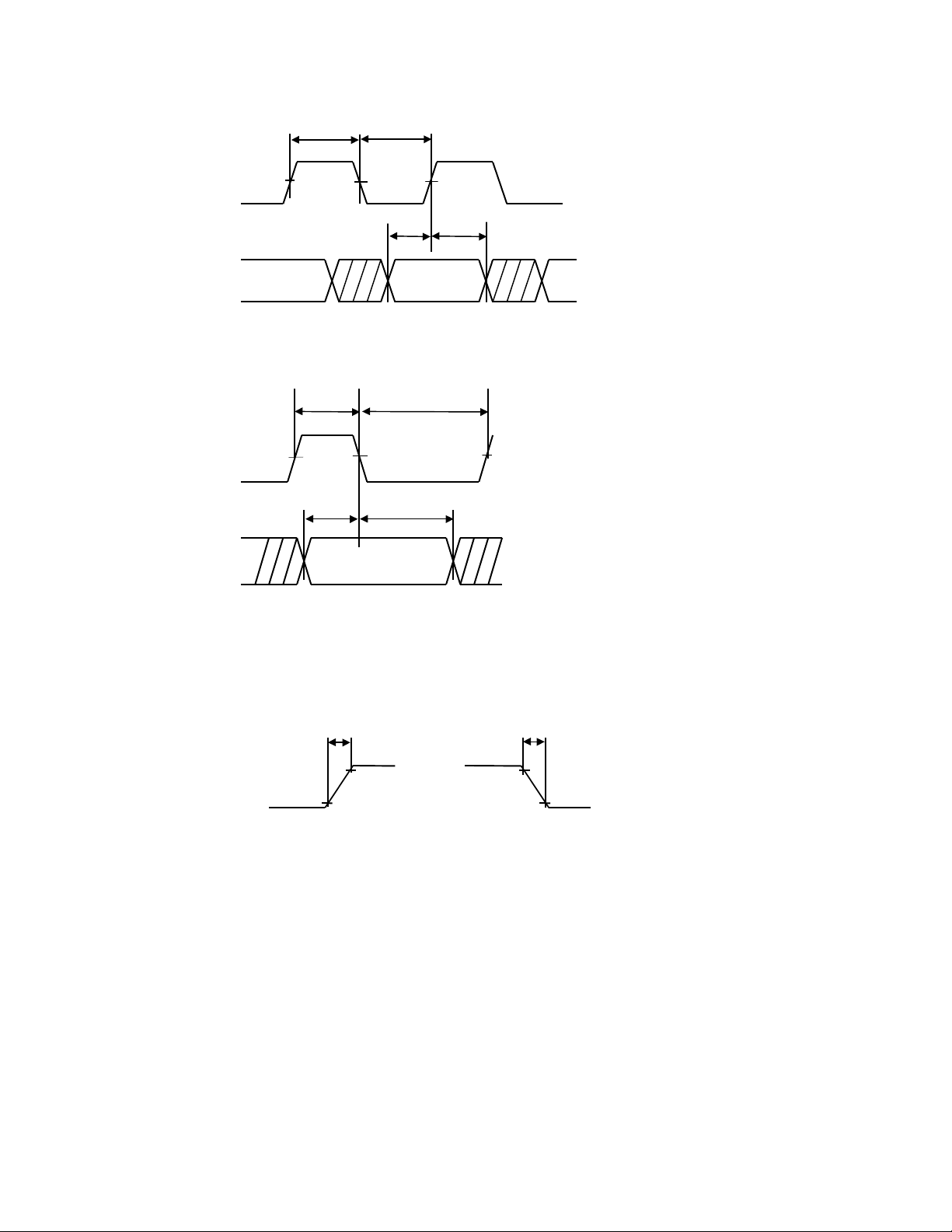
50%
RPOS/RNEG
50%
TPOS/TNEG
t
pwho
t
50%
pwlo
t
sur
50%
t
50%
Fig.1 Receiver Timing
t
t
pwhi
pwli
50%
t
sut
t
ht
50%
hr
50%
Fig.2 Transmitter Timing
t
r
t
f
90% 90%
10% 10%
Fig.3 Rise and Fall Times
(RCLK, RPOS, RNEG, TCLK, TPOS, TNEG)
Page 14

ASAHI KASEI [AK2546]
AC CHARACTERISTICS (Parallel Port)
Parameter Symbol Min Typ Max Units Condition
Read/Write Cycle tcyc 250 ns
Motorola Mode
Address Setup Time t1 10 — — ns
Address Hold Time t2 10 — — ns
AS to DS Delay Time t3 20 — — ns
DS to AS Delay Time t4 20 — — ns
Read Data Delay Time t5 — — 40 ns
Read Data Hold Time t6 — — 20 ns
R/W Setup Time t7 10 — — ns
R/W Hold Time t8 10 — — ns
CS Setup Time t9 10 — — ns
CS Hold Time t10 15 — — ns
Write Data Setup Time t11 40 — — ns
Write Data Hold Time t12 20 — — ns
DS Pulse Width t13 100 — — ns
AS Pulse Width t14 20 — — ns
Address Invalid to DS Delay Time t15 0 — — ns
Intel Mode
Address Setup Time t21 10 — — ns
Address Hold Time t22 10 — — ns
ALE to WR Delay Time t23 20 — — ns
WR to ALE Delay Time t24 20 — — ns
RD to ALE Delay Time t25 20 — — ns
Read Data Delay Time t26 — — 40 ns
Read Data Hold Time t27 — — 20 ns
CS Setup Time t28 10 — — ns
CS Hold Time t29 15 — — ns
Write Data Setup Time t30 40 — — ns
Write Data Hold Time t31 20 — — ns
RD Pulse Width t32 100 — — ns
WR Pulse Width t33 100 — — ns
ALE Pulse Width t34 20 — — ns
Address Invalid to RD Delay Time t35 0 — — ns
Notes) CL= 50pF on AD0-AD7. All of the timing is specified at 50%VDD.
Page 15
ASAHI KASEI [AK2546]
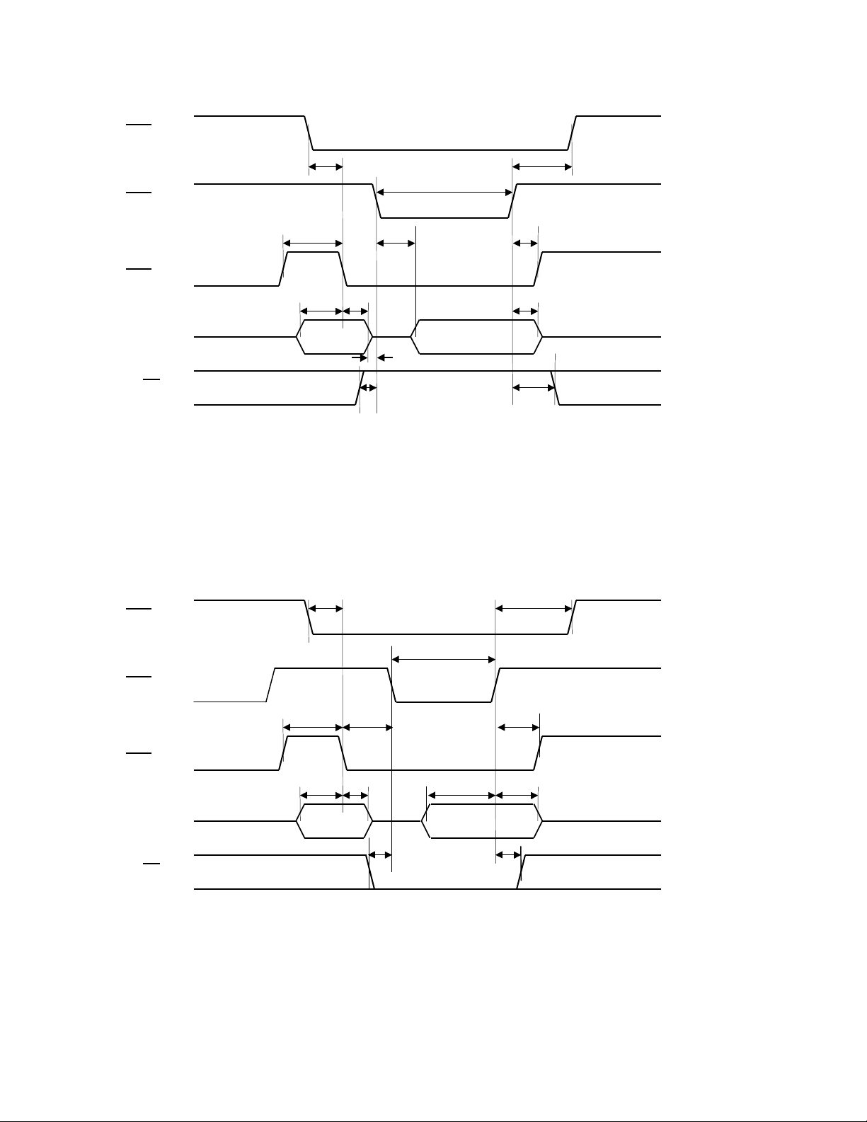
CSDSAS
AD7-0
R/W
Address
Data
t1t2t13t8t6t7t9
t10
CSDSAS
AD7-0
R/W
Address
Data
t1t2t3
t13
t12t7t9
t10
t8
t14
t11
t14t5t4t4t15
Motorola Mode(READ)
Motorola Mode(WRITE)
Page 16
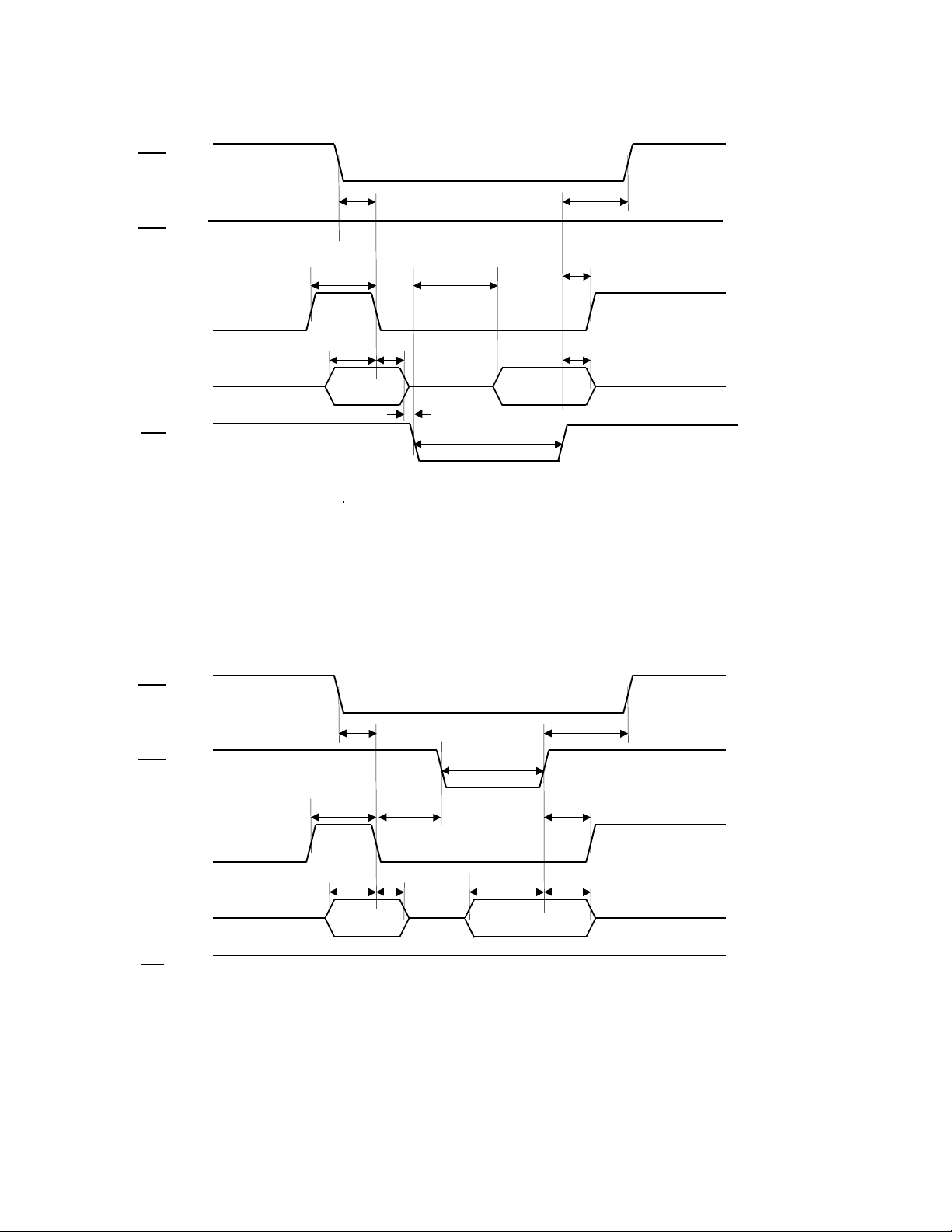
ASAHI KASEI [AK2546]
CSWRALE
AD7-0
RD
Address
Data
t21
t22
t34
t26
t27
t28
t29
CSWRALE
AD7-0
RD
Address
Data
t21
t22
t31
t28
t29
t30
t33
t24
t32
t25
t34
t23
t35
Intel Mode(READ)
Intel Mode(WRITE)
Page 17
ASAHI KASEI [AK2546]
REGISTER DESCRIPTION
REGISTER MAP
*A7-A4=“0”
Address Function
A3 A2 A1 A0
0 0 0 0
0 0 0 1
0 0 1 0
0 0 1 1
0 1 1 0
0 1 1 1
Bit7
<AD7>
LOS7
(1)
LOTC7
(1)
MLOS7
(1)
MLOTC7
(1)
LENG31
(0)
LENG32
Bit6
<AD6>
LOS6
(1)
LOTC6
(1)
Mask Control Register (WRITE/READ)
MLOS6
(1)
MLOTC6
(1)
Channel Control Register (WRITE/READ)
LENG21
(0)
LENG22
Bit5
<AD5>
Status Register (READ ONLY)
LOS5
(1)
LOTC5
(1)
MLOS5
(1)
MLOTC5
(1)
LENG11
(0)
LENG12
Bit4
<AD4>
LOS4
(1)
LOTC4
(1)
MLOS4
(1)
MLOTC4
(1)
RLOOP1
(0)
RLOOP2
LOTC3
MLOS3
MLOTC3
LLOOP1
LLOOP2
<AD3>
LOS3
Bit3
(1)
(1)
(1)
(1)
(0)
Bit2
<AD2>
LOS2
(1)
LOTC2
(1)
MLOS2
(1)
MLOTC2
(1)
POLN1
(1)
POLN2
Bit1
<AD1>
LOS1
(1)
LOTC1
(1)
MLOS1
(1)
MLOTC1
(1)
MSK1
(1)
MSK2
Bit0
<AD0>
0
LOMC
(1)
RDEN
(0)
MLOMC
(1)
PD1
(1)
PD2
1 0 0 0
1 0 0 1
1 0 1 0
1 0 1 1
1 1 0 0
(0)
LENG33
(0)
LENG34
(0)
LENG35
(0)
LENG36
(0)
LENG37
(0)
(0)
LENG23
(0)
LENG24
(0)
LENG25
(0)
LENG26
(0)
LENG27
(0)
(0)
LENG13
(0)
LENG14
(0)
LENG15
(0)
LENG16
(0)
LENG17
(0)
(0)
RLOOP3
(0)
RLOOP4
(0)
RLOOP5
(0)
RLOOP6
(0)
RLOOP7
(0)
(0)
LLOOP3
(0)
LLOOP4
(0)
LLOOP5
(0)
LLOOP6
(0)
LLOOP7
(0)
POLN3
POLN4
POLN5
POLN6
POLN7
*Other address is reserved.
* Initial value is in ( ).
*“<>” show I/O pin name. Address A0-A3 should be input via AD0-AD 3 pins.
(1)
(1)
(1)
(1)
(1)
(1)
(1)
MSK3
(1)
MSK4
(1)
MSK5
(1)
MSK6
(1)
MSK7
(1)
(1)
PD3
(1)
PD4
(1)
PD5
(1)
PD6
(1)
PD7
(1)
Page 18
ASAHI KASEI [AK2546]
STATUS REGISTER
Symbol Description
LOSx
(x=1 to 7)
LOTCx
(x=1 to 7)
LOMC Loss of MCLK alarm. Read only register.
Loss of signal alarm for channel x. Read only register.
When the loss of signal is detected, LOSx is set High.
Loss of TCLK alarm for channel x. Read only register.
When the loss of TCLKx is detected, LOTCx is set High.
When the loss of MCLK is detected, LOMC is set High.
MASK CONTROL
Symbol Description
MLOSx
(x=1 to 7)
MLOTCx
(x=1 to 7)
MLOMC Mask loss of MCLK alarm.
Mask loss of signal alarm for channel x.
MLOSx is active-high to prevent LOSx from setting INT output “high”.
It is possible to read LOSx register regardless of the status of MLOSx.
Initial value is “high”.
Mask loss of TCLK alarm for channel x.
MLOTCx is active-high to prevent LOTCx from setting INT output “high”.
It is possible to read LOTCx register regardless of the status of MLOTCx.
Initial value is “high”.
MLOMC is active-high to prevent LOMC from setting INT output “high”.
It is possible to read LOMC register regardless of the status of MLOMC.
Initial value is “high”. When the loss of MCLK is detected, LOSx register
and LOSx pins are set “high” at the same time. Therefore all MLOSx
register must be set “high” to prevent loss of MCLK from setting INT
output. In this case, LOMC can be read.
CHANNEL CONTROL REGISTER
Symbol Description
LENGyx The generated transmit pulse in channel x provides the appropriate pulse
shape for line length from a DSX-1 cross connect through the setting of this
register as shown below in Table 1.
RLOOPx/
LLOOPx
POLNx This register as shown in Table 3 controls TIPx/RINGx output polarity.
PDx PDx is active-high to set the corresponding transceiver in power down
MSKx MSKx is active-high to prevent LOSx or LOTCx from setting INT output
RDEN RDEN is active-high to prevent RCLK, RPOS, and RNEG output from
Loopback mode of channel x is activated through the setting of these
registers as shown below in Table 2.
Initial value is “high”.
mode.
The impedance between TTIP and TRING is set to 30kΩ(typ). LOSx goes
“high” in power down mode. Initial value is “high”.
“high”. Initial value is “high”.
forcing to “low” or “high” by the detection of Loss of signal. Initial value is
“low”.
Page 19

ASAHI KASEI [AK2546]
Table 1. Pulse Shape Control
LENG3x LENG2x LENG1x Line Length
0 0 0 0-133feet (Initial Value)
0 0 1 133-266feet
0 1 0 266-399feet
0 1 1 399-533feet
1 0 0 533-655feet
Table 2. Loopback mode Select
RLOOPx LLOOPx Function
0 0 Normal (Initial value)
0 1 Local Loop back
1 0 Remote Loop back
1 1 Inhibited
Table 3. TIPx/RINGx Polarity Control
POLNx POSx/NEGx TIPx/RINGx
0 space1
1 mark
0 mark0
1 space
Page 20

ASAHI KASEI [AK2546]
OUTPUT CONTROL
*: don’t care
LOS: LOSx output and LOSx register
Reset, Loss of MCLK, Power down
LoopbackRESET MCLK PD
Local Remote
0 * * * * * * * * 0(Note 1) 0 0 1
1 loss * * * 1 * * * 0 0 0 1
1 loss * * * 0 * * * 0 0 1 1
1 clocked 1 * * 1 * * * 0(Note 1) 0 0 1
1 clocked 1 * * 0 * * * 0(Note 1) 0 1 1
POLN RDEN TCLK Receive
signal
TTIP
TRING
RCLK RPOS
RNEG
Normal Operation(RESET=1, MCLK: Clocked, PD=0)
Loopback
Local Remote
0 0 1 * clocked in TPOS
0 0 1 0 clocked loss TPOS
0 0 1 * loss in 0 RCLK RTIP
0 0 1 0 loss loss 0 0 0 1
POLN RDEN TCLK Receive
signal
TTIP
TRING
TNEG
TNEG
RCLK RPOS
RNEG
RCLK RTIP
RRING
0 0 1
RRING
LOS
LOS
0
0
0 0 1 1 clocked loss TPOS
TNEG
0 0 1 1 loss loss 0 RCLK RTIP
0 0 0 * clocked in TPOS
TNEG
0 0 0 0 clocked loss TPOS
TNEG
0 0 0 * loss in 0 RCLK RTIP
0 0 0 0 loss loss 0 0 1 1
0 0 0 1 clocked loss TPOS
TNEG
0 0 0 1 loss loss 0 RCLK RTIP
RCLK RTIP
RRING
RRING
RCLK RTIP
RRING
0 1 1
RRING
RCLK RTIP
RRING
RRING
1
1
0
0
1
1
Page 21
ASAHI KASEI [AK2546]
Remote Loopback(RESET=1, MCLK: Clocked, PD=0)
Loopback
Local Remote
0 1 1 * * in
0 1 1 0 * loss
0 1 1 1 * loss
0 1 0 * * in
0 1 0 0 * loss
0 1 0 1 * loss
POLN RDEN TCLK Receive
signal
Local Loopback(RESET=1, MCLK: Clocked, PD=0)
Loopback
Local Remote
POLN RDEN TCLK Receive
signal
TTIP
TRING
RTIP
RRING
RTIP
RRING
RTIP
RRING
RTIP
RRING
RTIIP
RRING
RTIP
RRING
TTIP
TRING
RCLK RPOS
RNEG
RCLK
0 0 1
RCLK
RCLK
0 1 1
RCLK
RCLK RPOS
RTIP
RRING
RTIP
RRING
RTIP
RRING
RTIP
RRING
RNEG
LOS
0
1
0
1
LOS
1 0 1 * clocked in TPOS
TNEG
1 0 1 * clocked loss TPOS
TNEG
1 0 1 * loss in 0 0 0 0
1 0 1 * loss loss 0 0 0 1
1 0 0 * clocked in TPOS
TNEG
1 0 0 * clocked loss TPOS
TNEG
1 0 0 * loss in 0 0 1 0
1 0 0 * loss loss 0 0 1 1
TCLK
(Note 2)
TCLK
(Note 2)
TCLK
(Note 2)
TCLK
(Note 2)
TPOS
TNEG
TPOS
TNEG
TPOS
TNEG
TPOS
TNEG
Note 1) The impedance between TTIP and TRING is 30kΩ(typ).
Note 2) The phase of the TCLK satisfies receive output timing.
0
1
0
1
Page 22

ASAHI KASEI [AK2546]
THEORY OF OPERATION
Loss of signal
Loss of signal in channel x is reported by setting LOSx register “high”.
The receiver will indicate loss of signal upon receiving 175 consecutive zeros or detecting input
level being below the threshold (ALOS).
LOSx returns to “low” when the received signal returns to 12.5% ones density and not including
100 consecutive zeros. (GR-820)
When Loss of Signal is detected in channel x, LOSx register is set “high” and LOSx pin becomes
“high”. When LOSx is set “high”, interrupt will be issued on INT pin if MLOSx is “low”. LOSx
pin becomes high regardless of MLOSx status. MLOSx is active-high and masks LOSx interrupt.
LOSx registers and LOSx pins represent the current status of received signal regardless of the
MLOSx status.
Loss of TCLK
Loss of TCLKx is reported by setting LOTCx “high”. When LOTCx is set “high”, INT output
becomes “high” if MLOTCx is “low”. MLOTCx is active-high and masks LOTCx interrupt.
LOTCx represents the current status of TCLKx and can be read regardless of MLOTCx status.
When Loss of TCLKx is detected, TTIPx/TRINGx will be forced to “0”.
Loss of MCLK
Loss of MCLK is reported by setting LOMC “high”. When LOMC is set “high”, INT output
becomes “high” if MLOMC is “low”. MLOMC is active-high and masks LOMC interrupt.
LOMC represents the current status of MCLK and can be read regardless of MLOMC status.
When the loss of MCLK is detected, LOSx register and LOSx pin goes “high” at the same time.
Therefore all MLOSx register must be set to “high” to prevent loss of MCLK from setting INT
output
INT output
INT output becomes “high” when the alarm is reported to any one of LOSx, LOTCx or LOMC
registers. This pin can be masked by MLOSx, MLOTCx or MLOMC registers.
Local Loopback
In Local Loopback mode, TPOSx, TNEGx, TCLKx signals are looped back to RPOSx, RNEGx,
RCLKx output. RTIPx, RRINGx inputs are ignored but loss of signal detection is active.
The transmitter in channel x outputs TTIPx, TRINGx normally.
Remote Loopback
In Remote Loopback mode, RTIPx/RRINGx signals are looped back to TTIPx/TRINGx output.
The receiver in channel x output RPOSx, RNEGx, RCLKx normally and detect loss of signal.
TPOSx, TNEGx, TCLKx inputs are ignored.
Page 23

ASAHI KASEI [AK2546]
AK2546
AK2546
RECOMMENDED EXTERNAL CIRCUIT
Transmit Circuit
VDD
Received Circuit
TTIPx
TRINGx
RTIPx
RRINGx
VDD
VDD
VDD
C1
C1=0.47µF
R3
R4
1:2
R1
R2
2:1
R1=R2=68Ω
R3=R4=130Ω
Recommended Transformer Specification
Turns
Ratio
(Typ)
Tx 1:2 720µH 0.3µH 30pF 0.6Ω 1.2Ω
Rx 1:2 720µH 0.3µH 30pF 0.6Ω 1.2Ω
Primary
Inductance
(Min)
Leakage
Inductance
(Max)
Interwinding
Capacitance
(Max)
DCR
(Max)
pri sec
Page 24

ASAHI KASEI [AK2546]
Reference current circuit
To determine input reference current, connect 12kΩ±1% resistor.
AK2546
R1
BGREF
R1=12kΩ±1%
Power Supply
To attenuate the power supply noise, connect capacitors between VDD and VSS respectively.
The value of the capacitance AK2546 need depend on the condition of the power supply line.
Please decide the value of the capacitance after your evaluation.
AK2546
C1
Pin name C1
RAVDD1-RAVSS1, RAVDD2-RAVSS2, BVDD-BVSS,
TAVDD1-TAVSS1, TAVDD2-TAVSS2
TVDD1-TVSS1, TVDD2-TVSS2, TVDD3-TVSS3, TVDD4-TVSS4,
VDD
1µF
0.01µF
TVDD5-TVSS5, TVDD6-TVSS6, TVDD7-TVSS7, IOVDD1IOVSS1, IOVDD2-IOVSS2, DVDD1-DVSS1, DVDD2-DVSS2,
PVDD-PVSS
Page 25

ASAHI KASEI [AK2546]
Recommended conditions for PCB board
For the performance of noise and heat, the board design must be taken care.
Recommended conditions for PCB board is shown below.
Recommended conditions:
Multilayerboard with more than two VDD or GND layer
Please design the rest of pattern for GND
Page 26

ASAHI KASEI [AK2546]
PACKAGE
144pin LQFP
OUTPUT DIMENSIONS
22.0
20.0
73108
Max
1.70
109
144
1.40
72
AK2546
22.0
XXXXXXX
20.0
JAPAN
37
1
0.50
0.20
0.10 M
36
0.07
0.04
0~10º
0.17±
0.10
0.10
0.50±0.1
Page 27

ASAHI KASEI [AK2546]
IMPORTANT NOTICE
• These products and their specifications are subject to change without notice. Before considering
any use or application, consult the Asahi Kasei Microsystems Co., Ltd. (AKM) sales office or
authorized distributor concerning their current status.
• AKM assumes no liability for infringement of any patent, intellectual property, or other right in the
application or use of any information contained herein.
• Any export of these products, or devices or systems containing them, may require an export
license or other official approval under the law and regulations of the country of export pertaining
to customs and tariffs, currency exchange, or strategic materials.
• AKM products are neither intended nor authorized for use as critical components in any safety, life
support, or other hazard related device or system, and AKM assumes no responsibility relating to
any such use, except with the express written consent of the Representative Director of AKM. As
used here:
(a) A hazard related device or system is one designed or intended for life support or maintenance
of safety or for applications in medicine, aerospace, nuclear energy, or other fields, in which
its failure to function or perform may reasonably be expected to result in loss of life or in
significant injury or damage to person or property.
(b) A critical component is one whose failure to function or perform may reasonably be expected
to result, whether directly or indirectly, in the loss of the safety or effectiveness of the device
or system containing it, and which must therefore meet very high standards of performance
and reliability.
• It is the responsibility of the buyer or distributor of an AKM product who distributes, disposes of, or
otherwise places the product with a third party to notify that party in advance of the above content
and conditions, and the buyer or distributor agrees to assume any and all responsibility and
liability for and hold AKM harmless from any and all claims arising from the use of said product in
the absence of such notification.
 Loading...