

Page 1
ASAHI KASEI [AK2048]
2M
2M CMI
2M2M
CMI Transceiver
CMI CMI
AK2048D
AK2048D
AK2048DAK2048D
Transceiver
TransceiverTransceiver
- 2.048Mbps CMI Interface
- CLOCK & DATA Recovery function
- Loss of Lock Detection
- Loss of Signal Detection
- Transmitter Pulse Shape
- Single 5.0V±5% Operation
- Low Power Consumption: 400mW (TYP)
- Package: 44pin QFP
TXA
TXA
TXATXA
TXB
TXB
TXBTXB
DRIVER
RRRRXA
XA
XAXA
RRRRXXXXBBBB
VREF
RESET
FEATURES
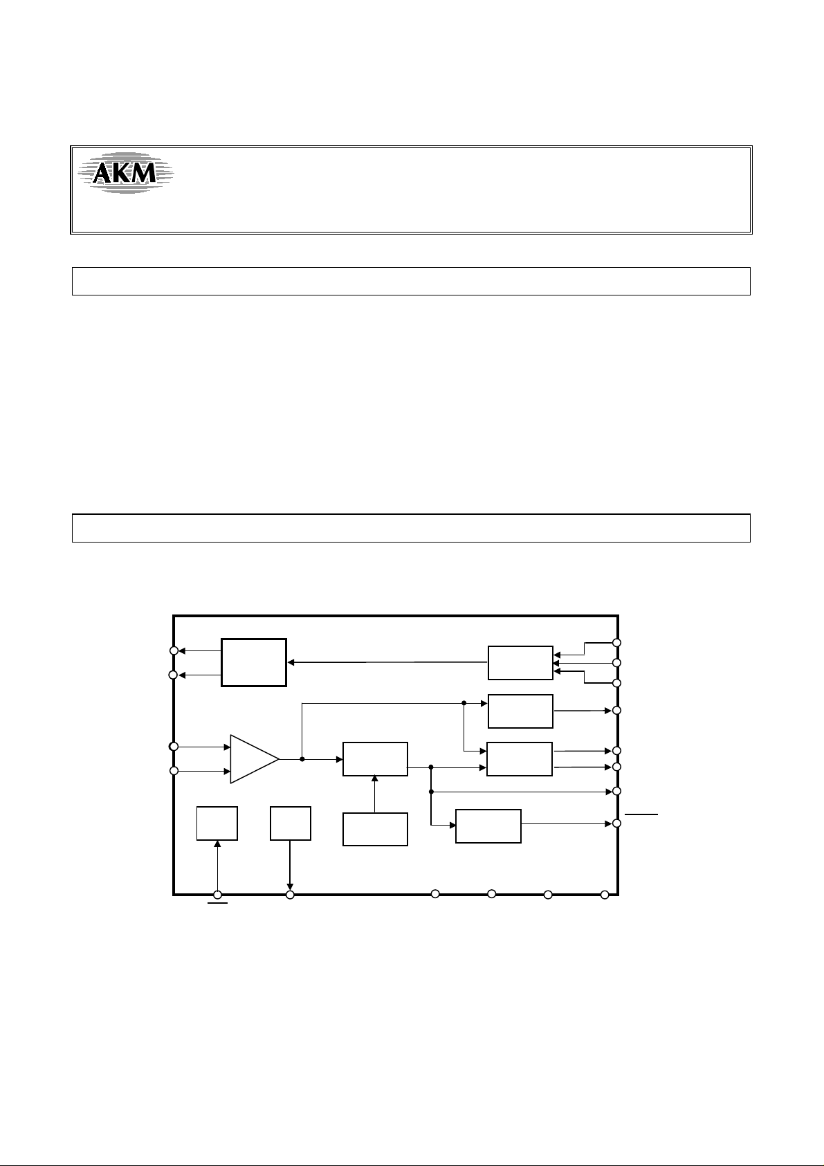
BLOCK DIAGRAM
CLOCK
RECOVER
CALIB
ENCODER
DECODER
LOCK
CMI
LOS
CMI
TDATA
TDATA
TDATATDATA
TCLK
TCLK
TCLKTCLK
TCRV
TCRV
TCRVTCRV
LOS
LOS
LOSLOS
RDATA
RDATA
RDATARDATA
RCRV
RCRV
RCRVRCRV
RCLK
RCLK
RCLKRCLK
LOCK
LOCK
LOCKLOCK
RST
RST
RSTRST
REF25
REF25 RRRRVDD
REF25REF25
2M CMI Transceiver Block Diagram
MS0073-E-00 2001/01 1
VDD RVSS
VDDVDD
RVSS TVDD
RVSSRVSS
TVDD TVSS
TVDDTVDD
TVSS
TVSSTVSS
Page 2
ASAHI KASEI [AK2048]
GENERAL DESCRIPTI O NS
AK2048D is the 2.048Mbps CMI interface CMOS LSI for CMI interface card. It includes Clock and
Data Recovery, L i ne Dr i ver, LO S Det ect o r , etc.
Build in PLL clock recovery circuit eliminates the correlation of the frequency deviation due to the
uneven quality of the devices and a secular change.
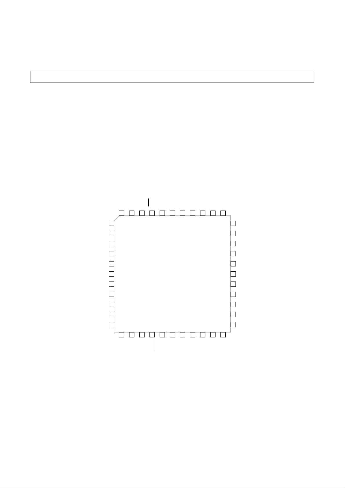
PIN ASSIGNMENTS
44pin QFP
NC
NC
NC
NC
RVDD
LOS
NC
NC
NC
NC
NC
NC
NC
NC
RXA
33
NC
32
REF25
31
NC
30
RXB
29
NC
28
NC
27
TXA
26
TVDD
25
TVSS
24
TXB
23
RDATA
RCLK
RCVR
NC
NC
NC
NC
NC
TDATA
TCLK
TCRV
NC
NC
RVSS
RST
44 43 42 41 40 39 38 37 36 35 34
1
2
3
4
5
(TOP VIEW)
(TOP VIEW)
6
(TOP VIEW)(TOP VIEW)
7
8
9
10
11
12 13 14 15 16 17 18 19 20 21 22
TEST1
TEST2
NC
LOCK
MS0073-E-00 2001/01 2
Page 3
ASAHI KASEI [AK2048]
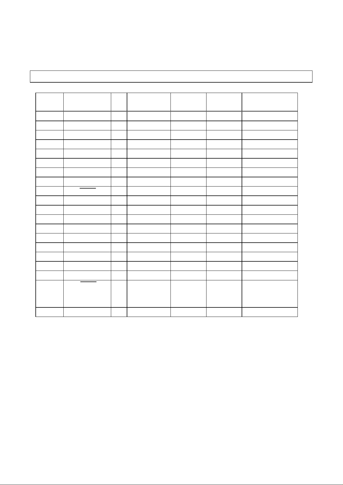
PIN ASSIGNMENTS
Pin No. Pin Name I/O Type AC Load
(MAX)
1
2
3
9
10
11
13
14
15
16
23
24
25
26
29
31
33
40
41
42
The other pins (4-8,12,17-22,27,28,30,32,34-39,43,44) are NC pins.
RDATA O TTL ≤15pF
RCLK O TTL ≤15pF
RCRV O TTL ≤15pF
TDATA I TTL
TCLK I TTL
TCRV I TTL
TEST1 - *2)
TEST2 - *2)
LOCK O TTL ≤15pF
LOS O TTL ≤15pF
TXB O Analog ≤15pF *1)
TVSS -
TVDD -
TXA O Analog ≤15pF *1)
RXB I Analog
REF25 O Analog 1µF(typ)
RXA I Analog
RVDD -
RST I TTL Pulled up to VDD
RVSS -
DC Load
(MIN)
≥4kΩ
≥4kΩ
≥4kΩ
≥4kΩ
≥4kΩ
Comment
by the internal
register (50KΩmin)
NC pins are recommended to connect to VSS to avoid noise problem.
*1) TXA, TXB can drive 11 0Ω connected between these pins .
*2) Must be ope n .
MS0073-E-00 2001/01 3
Page 4
ASAHI KASEI [AK2048]
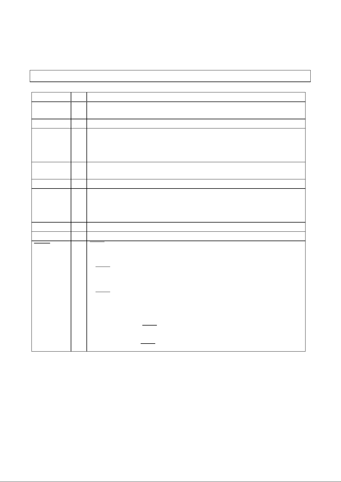
PIN DESCRIPTIONS
Pin Name I/O Function
RDATA O
RCLK O
RCRV O
TDATA I
TCLK I
TCRV I
TEST1 NC
TEST2 NC
LOCK O
Receive Data output recovered from the incoming data. Delay time from the incoming
data to the RDATA is about 1.25bit. Output on the rising edge of RCLK.
Receive Clock Output recovered from the incoming data.
CRV (Code Rule Violation) output pin .
When AK2048D detects the CRV of CMI codes from in the coming data, RCRV goes
to “high” synchronized with the violation data. CRV is detected for both “0” data and
“1” data. Refer to Fig.6, 11
Transmit Data Input pin.
Input on the falling edge of TCLK.
Transmit Clock Input pin.
If this input is “high”, AK2048D generates CR V in the transm i t d ata.
CRV is generated for both “0”data and “1”data. “High” input TCRV is accepted until 5
clocks duration. If the duration of “High” input is longer than 6 clocks, TCRV input
after 6th clock is ignored. Refer to Fig.4, 11
Test pin. Should be floated.
Test pin. Should be floated.
LOCK indicates the PLL st atus whether PLL is in the LOCK s tatus or PLL is in the
UNLOCK status.
LOCK status
LOCK becomes “Low” when the sampled RCLK are all “Low” during the consecutive
32 RXA-RXB sample clock duration.
UN LOCK status
LOCK becomes “High” when the following both conditions are satisfied.
The sampled RCLK are “High” m or e than 5 clocks in the frame of the consecutive
-
256 RXA-RXB clock duration.
And the above happens in the 5 consecutive frames.
-
In another condition, LOCK keeps the current output status without change.
The output timing of this signal is asynchronous with RCLK.
When RST is “Low”, LOCK is fixed to “High”.
MS0073-E-00 2001/01 4
Page 5
ASAHI KASEI [AK2048]
Pin Name I/O
LOS O
TXB O
TVSS TVDD TXA O
RXB I
REF25 O
RXA I
RVDD RST O
RVSS -
LOS goes High within 12usec after AK2048D detects that the amplitude of the RXB
input signal is lower than 135mVpp(typ). Output on the rising edge of RCLK.
Transmit CMI signal output. TXA is to CMI+, and TXB is corresponds to CMI-.
Delay time from TDATA to TXB is about 1bit.
Negative power supply 0V
Positive power supply 5V
Transmit CMI signal output. TX A is to CMI+, and T XB is corresponds to CMI-.
Delay time from TDATA to TXA is about 1bit.
Receive CMI signal input. RXA is to CMI+, and RX B is corresponds to CMI -.
Output reference voltage (about 2.5V) in order to decide middle point of input signal
(RXA-RXB). Connected to middl e point of the external equ a l iz er.
Receive CMI signal input. RXA is to CMI+, and RX B is corresponds to CMI -.
Positive power supply .
“Low” input reset the calibration circuit and forces LOCK output “High” and
TXA-TXB output “High-Z”. When this input rise, PLL calibration restarts.
Please set open or connect to VDD when not using.
Negative power supply 0V
5V
Function
MS0073-E-00 2001/01 5
Page 6

ASAHI KASEI [AK2048]
ABSOLUTE MAXIMUM RATINGS
Parameter Symbol Min Typ Max Units Conditions
DC Supply DVDD
-0.3 6.0 V
TVDD
Input Voltage VIN RVSS-0.3 RVDD+0.3 V
Input Current 1 I
Input Current 2
10 mA *1)
IN1
I
200 mA
IN2
(TXA, TXB, RXA, RXB)
C
Storage Temperature Tstg -65 150
°
*1) Except for TXA, TXB, RXA, RXB
RECOMMENDED OPERATING CONDITIONS
Parameter Symbol min typ max Unit Conditions
DC Supply RVDD
4.75 5.0 5.25 V
TVDD<RVDD+0.3V
TVDD
C
Ambient Operating
Ta 0 25 +80
°
Temperature
PD1(RVDD) 150 300 mW
Power Consumption
PD2(TVDD) 250 300 mW
110Ω LOAD
DC CHARACTERISTICS
ELECTRICAL CHARACTERIS TI C S
Condition: VDD =5.0 V±5%, VSS=0V,Ta=0~80°C
Parameter Symbol min typ max Unit Conditions
Digital High-lev el input volta ge VIH 2.4 V
Digital Low-leve l input volt age VIL 0.8 V
=-40µA *1)
Digital High-Lev el outp ut volta ge VOH 2.4 V
Digital Low-leve l outp ut volta ge VOL 0.5 V I
Input leak current 1 10
Input leak current 2 100
µ
µ
I
OUT
=1.6mA *1)
OUT
A
Without RST, TEST1
A
RST, TEST1
*1) When CMOS load is connected, output CMOS logic level.
MS0073-E-00 2001/01 6
Page 7

ASAHI KASEI [AK2048]
TRANSMITTER
Parameter Symbol min typ max Unit Comments
Va 2.55 3.3 3.90
Output signal level
Rise/Fall Time Tr, Tf 20 50 ns Refer to Fig.1, 2
Pulse duty of transmit output 43 50 57 %
Delay time from T D AT A to T XA,TXB Ttd 1 Bit *3)Refer to Fig.4
*1) The duty cycl e of TCLK 50%±4%.
*2) Duty cycle = Tpwh / (Tpwh + Tpwl) × 100%
*3) Signal output delay = (1bit logical delay) + (internal propagation delay)
VpeakH 4.05
VpeakL 2.55
Ω
56
Refer to Fig.1, 2
Vp-p
*1), *2)
Refer to Fig.3
TXA
Ω
110
VpeakH
Va
VpeakL
TXB
Ω
56
Transmit output amplitude
is specified at this point.
(Va, VpeakH, VpeakL)
Fig.1 Measurement c ircuit
Fig.2 Rise and fall times
0.8Va
Tr,Tf
MS0073-E-00 2001/01 7
Page 8

ASAHI KASEI [AK2048]
Tpwh Tpwl
50%
Fig.3 Transmit outp ut pulse dut y
TCLK
TCRV
TDATA
TXA-TXB
Ttd
Fig.4 Data i nput to s ignal output delay time
BA
CD
AC
B
The shaded portion is
CRV bit
MS0073-E-00 2001/01 8
Page 9

ASAHI KASEI [AK2048]
RECEIVER
Parameter Symbol min typ max Unit Comments
REF25 output VREF 2.0 2.5 3.0 V Iout<IuA *1)
Signal loss threshold level Vth 85 135 185 mVp-p RXB terminal
Signal loss detection time TALM 10 12 usec Fig.5
Sensitivity 0.2 4.0 Vp-p
Input jitter tolerance 0.15 UIp-p Jitter frequency
20KHz~100KHz
PSRR (Line Length 400m) 400 mVp-p *2)
S/X tolerance
Line Length 400m
0m
Signal input to Data output
delay time
2
12
dB
frequency 1.9MHz
dB
*2)
Trd 1.25 bit Fig.6
*3)
RCLK Output Jitter 3 nsp-p *4)
*1) Reference output of fixed equalizer.
15
*2) The amplitude of input data is 3. 0±0.75Vp-p and the data pattern is 2
-1.
*3) Data output delay = (1.25bit logical delay) + (internal propagation delay)
*4) Data patt ern is “all space” wit h CRV every 8kHz cycle.
RxA
RxA
RxARxA
135mVp-p
RxB
RxB
RxBRxB
LOS
LOS
LOSLOS
135mVp-p REF25
135mVp-p135mVp-p
TALM
TALM
TALMTALM
50%
50%
50%50%
REF25
REF25REF25
Fig.5 LOS output s ignal
RXA
RXB
A
B
CE
RCLK
RCRV
RDATA
A
B
The shaded portion is
Trd
Fig.6 Delay time from RXA,RXB to RDATA
MS0073-E-00 2001/01 9
D
DC
CRV bit
Page 10

ASAHI KASEI [AK2048]
AC CHARACTERISTICS
Parameter
Parameter Pin
ParameterParameter
Input Clock
Frequency
Duty Cycle TCLK 46 50 54 % *1) Refer to Fig.7
Delay time from
TCLK rising to
TDATA, TCRV.
Output Clock
Frequency
Output Clock Duty RCLK 43 50 57 % *1) Refer to Fig.7
Delay time from
RCLK rising to
RDATA, RCRV.
Rise/Fall Time
Pin
Pin Pin
Name
Name
NameName
TCLK fin 2.048 MHz
TDATA
TCRV
RCLK fout 2.048 MHz
RDATA
RCRV
LOS
LOCK
RDATA
RCLK
RCRV
Symbol
Symbol min
SymbolSymbol
Tpd -58 58 ns Refer to Fig.8
Tpd -48 48 ns Refer to Fig.8
Tr, Tf
min typ
minmin
15 30 ns
15 ns
typ max
typtyp
max Unit
maxmax
Unit Condition
UnitUnit
Conditionssss
ConditionCondition
The bit rate of
received signal is
2.048Mbps
Refer to Fig.9
Delay time from
RCLK rising to L OS
*1) Duty: Tpwh/(Tpwh+Tpwl) × 100%
LOS Tpd -48 48 ns Refer to Fig.8
MS0073-E-00 2001/01 10
Page 11

ASAHI KASEI [AK2048]
,
V
V
p
TCLK
TDATA, RDATA
TCRV, RCRV
LOS
DD
4k
Tpwh Tpwl
50%
RCLK
50%
Fig.7 Clock timing
50%
Tpd
Fig. 8 Trans mitter Ti m ing
50%
50%
50%
Tr Tf
50%
OUTPUT PIN
Measurement p oint
15
90% 90%
10% 10%
SS
Fig.9 Rise and fall times and a condition of measurement.
MS0073-E-00 2001/01 11
Page 12

ASAHI KASEI [AK2048]
FUNCTIONAL DESCRIPTION
PLL calibration function
The calibration of PLL is caused in case of the following 3cases.
(1) Power on
(2) RST rising
(3) LOCK rising
(1) Power on
After th e power is on, the calibration is complete and LOCK goes to “Low ” in less than 63ms from
whichever the later happens, the input of signal (RXA-RX B) or th e rising edge of RST.
(2) RST rising
The calibration is complete and LOCK goes to “Low” in less than 38ms from whichever the later
happens, the input of signa l (RXA-RXB) or the rising edge of RST.
(3) LOCK rising
When the devi ce falls into unlock by some reasons and LOCK goes to “high”, calibration restarts.
The calibration is complete and LOCK goes to “Low” in less than 38ms from the rising edge of LOCK.
PLL pull in time after loss of signal
When LOS goes to “high” by loss of signal after the calibration, th e pull in of the PLL restarts by
signal input. If the device can pull in without cali bration, pull- in completes less than 200us.
In other case, LOCK goes to “high” and calibration restarts less than 2ms.
LOS signal
LOS goes to ”high”, when the amplitud e of RXB is less than 135 mVpp(typ) dur ing 16 bits (abou t 8us).
LOS signal goes to “Low”, when amplitude of RXB is more than 135mVpp(typ).
When the signal is lost during the calibration, LOS signal goes to “high” and the calibration circuit is
reset. The calibration restarts after LOS signal goes to “Low”.
MS0073-E-00 2001/01 12
Page 13

ASAHI KASEI [AK2048]
CRV (Code Rule Violation)
CMI code with violation is called as MD (Modified Dipulse) code. MD is refer to Fig.10. Generally
speaking, CRV (Code Rule Violation) is generated at co de “1”. But AK2048D genera tes the violation
for not only code “1”, but also code “0”. Violation of code “0” is refer to Fig.11.
CLOCK
NRZ
MD
Fig.10 MD code
violation
MARK(1)
SPACE(0)
CODE "0"
Violation of
CODE "0"
Fig.11 Viola ti on of CO DE “0”
MS0073-E-00 2001/01 13
Page 14

ASAHI KASEI [AK2048]
RECOMMENDED EXTERNAL CIRCUITS
VDD
CMI
input
R0 = 110
R1 = R2 = 56
C0 = 1 uF
1:1CT
Ω
output
Ω
R0
CMI
EQL.
VDD
1:1CT
C0
R1
R2
VDD
VSSVDD
RXA(33)
REF25(31)
RXB(29)
AK2048D
AK2048D
AK2048DAK2048D
TXA(26)
TXA(23)
VDD VDD
TVDD(25)
RVDD(40)
TVSS(24)
Fig.12 The example of the external circuits
It is recommended that Shott key diode in Fig 12 is connected for protection of latch-up.
RVSS(42)
MS0073-E-00 2001/01 14
Page 15

ASAHI KASEI [AK2048]
PACKAGE
18.2±0.4
18.2±0.4 14TYP
34
44
33
14TYP
XXXXYZZ
AK2048D
JAPAN
0.5MAX
23
22
12
0-15
1
0.4±0.1
MS0073-E-00 2001/01 15
1±0.16
11
1±0.4
2.9MAX
0.96TYP
0.15±0.05
15
Page 16

ASAHI KASEI [AK2048]
IMPORTANT NO TICE
•
These products and their specifications are subject to change without notice. Before considering
any use or application, consult the Asahi Kasei Microsystems Co., Ltd. (AKM) sales office or
authorized distributor conc erning their current status.
•
AKM assumes no liability for infringement of any patent, intellectual property, or other right in the
application or use of any infor mation containe d herein.
•
Any export of these products, or devices or systems containing them, may require an export license
or other official approval und er the law and regulations of the cou ntry of export pertaining to customs
and tariffs, currency exchange, or strategic materials.
•
AKM products are neither intended nor authorized for use as critical components in any safety, life
support, or other hazard related device or s ystem, and AKM assumes no responsibilit y relating to any
such use, except with the express written consent of the Representativ e Director of AKM. As used
here:
(a) A hazard related device or system is one designed or intended f or life support or maintenance of
safety or for applications in medicine, aerospace, nuclear energy, or other fields, in which its
failure to function or perform may reasonabl y be expected to result in loss of life or in significant
injury or damage to person or prop erty.
(b) A critical component is one whose failure to function or perform may reasonably be expected to
result, whether directly or indirectly, in the loss of the safety or effectiveness of the device or
system containing it, and which must therefore meet very high standards of performance and
reliability.
•
It is the responsibility of the buyer or distributor of an AKM product who distributes, disposes of, or
otherwise places the product with a third party to notify that party in advance of the above content
and conditions, and the buyer or distributor agrees to assume any and all responsibility and liabili ty
for and hold AKM harmless from any and all claims arising from the use of said product in the
absenc e of such no tif icatio n.
MS0073-E-00 2001/01 16
 Loading...