

Page 1
Ω
AIC3643
Built-in OVP White LED Step-Up Converter
FEATURES
Built-In Open Circuit Protection
Over Voltage Protection
Efficiency Up to 83% at VIN=4.2V, 3LEDs,
I
=20mA
LED
1.2MHz Fixed Switching Frequency
Drives Up to 5LEDs in series
2.5V to 5.5V Input Voltage
Low Supply Current: 150μA
Matches LED Current
Requires Tiny Inductor and Capacitors
TSOT-23-6, and SOT-23-6 Packages
DESCRIPTION
AIC3643 is a current-mode pulse-widthmodulation (PWM), step-up DC/DC converter
designed to drive white LEDs with a constant
current to provide backlight in hand-held devices.
Series connection of LEDs provides identical
LED currents resulting in uniform brightness.
This configuration eliminates the need of ballast
resistors. The built-in open load protection
prevents the damage resulting from an open
circuit condition. Also low 100mV feedback
voltage minimizes power loss in the current
setting resistor for better efficiency.
APPLICATIONS
Cellular Phones
PDAs
DSCs
Handheld Devices
White LED Display Backlighting
AIC3643 is a step-up PWM converter, which
includes an internal N-channel MOSFET switch
for high efficiency. The high switching frequency,
1.2MHz, allows the use of tiny external
components.
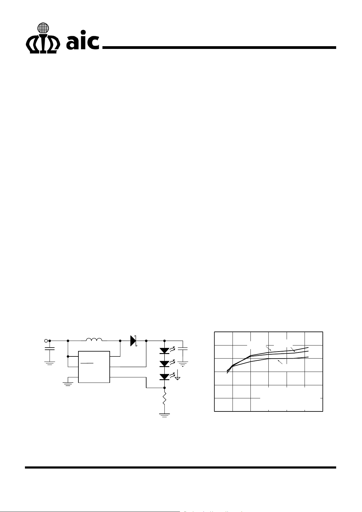
TYPICAL APPLICATION CIRCUIT
3.0~4.2V
C1
1μF
L1: GTSD31-6R8M, GOTREND
D1: SS0540, PAN JIT
C1: JMK107BJ105KA, TAIYO YUDEN
C2: GRM21BR61C335K, MURATA
L
6.8μH
VIN
SHDN
GND
AIC3643
SW
OVP
FB
Fig. 1 Li-Ion Powered Driver for Three White LEDs
D1
RFB
5
C2
3.3μF
20mA
AIC3643 is available in a space-saving TSOT23-6, and SOT-23-6 packages.
90
85
80
75
70
Efficiency (%)
65
60
0 5 10 15 20 25 30
VIN=4.2V
LED Current (mA)
VIN=3.6V
VIN=3V
3 LEDs, 6.8μH
L1: GTSD31-6R8M, GOTREND
D1: SS0540, PAN JIT
Test Circuit refer to Fig.1
Analog Integrations Corporation Si-Soft Research Center DS-3643G-01 20090820
3A1, No.1, Li-Hsin Rd. I, Science Park, Hsinchu 300, Taiwan, R.O.C.
TEL: 886-3-5772500 FAX: 886-3-5772510 www.analog.com.tw
1
Page 2
A
AIC3643
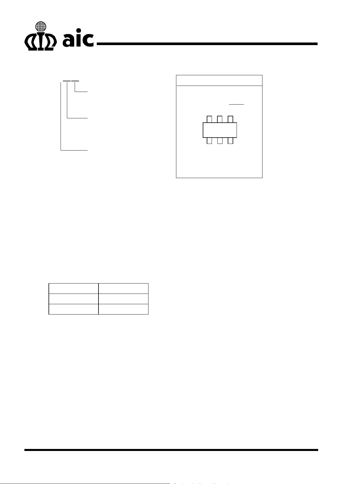
ORDERING INFORMATION
IC3643XXX XX
PIN CONFIGURATION
PACKING TYPE
TR: TAPE & REEL
BG: BAG
PACKAGE TYPE
G6: SOT-23-6
K6: TSOT-23-6
G: Green Package
Example: AIC3643GG6TR
in SOT-23-6 Green Package &
Tape & Reel Packing Type
SOT-23-6
TSOT-23-6
FRONT VIEW
OVP
5
2
GNDSW
SHDN
4
3
FB
VIN
6
3643G/3643K
1
Note: Pin1 is determined by orienting
the package marking as shown.
Marking
Part No. Marking
AIC3643GG6 3643G
AIC3643GK6 3643K
2
Page 3

AIC3643
ABSOLUTE MAXIMUM RATINGS
Input Voltage (VIN) 6V
SW Voltage
FB Voltage
SHDN
OVP Voltage
Operating Temperature Range
Storage Temperature Range
Maximum Junction Temperature
Lead Temperature (Soldering, 10 sec)
Thermal Resistance Junction to Case SOT-23-6
TSOT-23-6
Thermal Resistance Junction to Ambient SOT-23-6
TSOT-23-6
Absolute Maximum Ratings are those values beyond which the life of a device may be impaired.
Voltage 6V
–40°C to 85°C
–65°C to 150°C
33V
6V
34V
150°C
260°C
115°C/W
115°C/W
250°C/W
250°C/W
3
Page 4
AIC3643
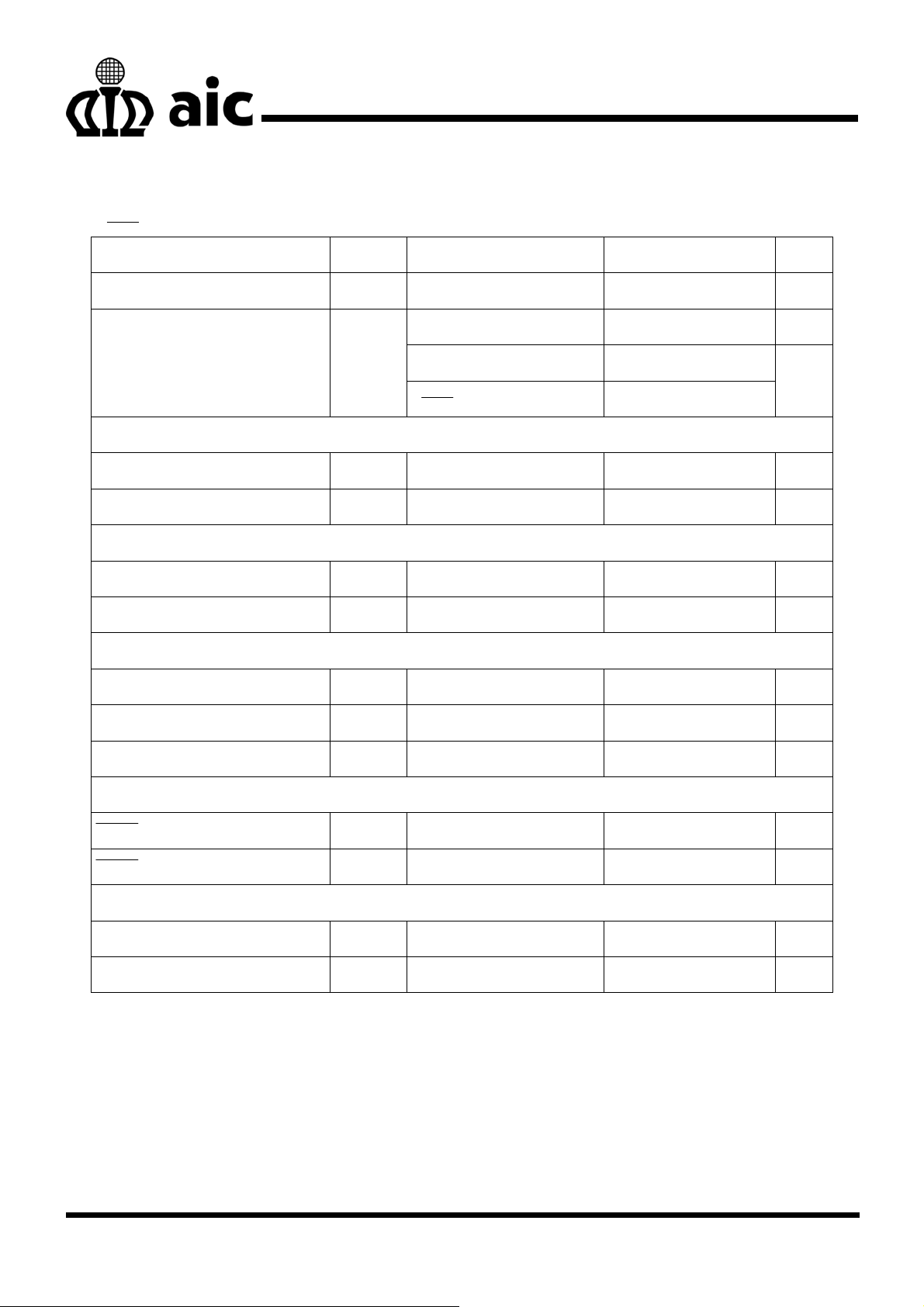
ELECTRICAL CHARACTERISTICS
(V
=1.5V, VIN=3V, TA=25°C, unless otherwise specified.) (Note 1)
SHDN
PARAMETER SYMBOL TEST CONDITIONS MIN TYP MAX UNIT
Operating Voltage VIN 2.5 5.5 V
Switching 1 3 mA
Supply Current IIN
Non switching 150 270
V
= 0V 0.1 1.0
SHDN
ERROR AMPLIFIER
V
Feedback Voltage
FB Input Bias Current
90 100 110 mV
FB
I
FB
V
FB
=100mV
1 nA
OSCILLATOR
Switching Frequency f
0.8 1.2 1.6 MHz
OSC
Maximum Duty Cycle D 91 94 %
μA
POWER SWITCH
SW ON Resistance R
Switch Leakage Current I
DS(ON)
SW(OFF)VSW
1.4 2.5 Ω
=33V 0.1 1 μA
Switch Current Limit IIL 0.65 1 A
CONTROL INPUT
SHDN Voltage High V
SHDN
Voltage Low V
ON 1.5 V
IH
OFF 0.3 V
IL
OVER VOLTAGE PROTECTION
OVP Input Resistance R
OVP Threshold V
0.8 1.2 1.6 MΩ
OVP
1V Hysteresis typical 22 28 32 V
OVP
Note 1: Specifications are production tested at TA=25°C. Specifications over the -40°C to 85°C operating
temperature range are assured by design, characterization and correlation with Statistical Quality
Controls (SQC).
4
Page 5
AIC3643
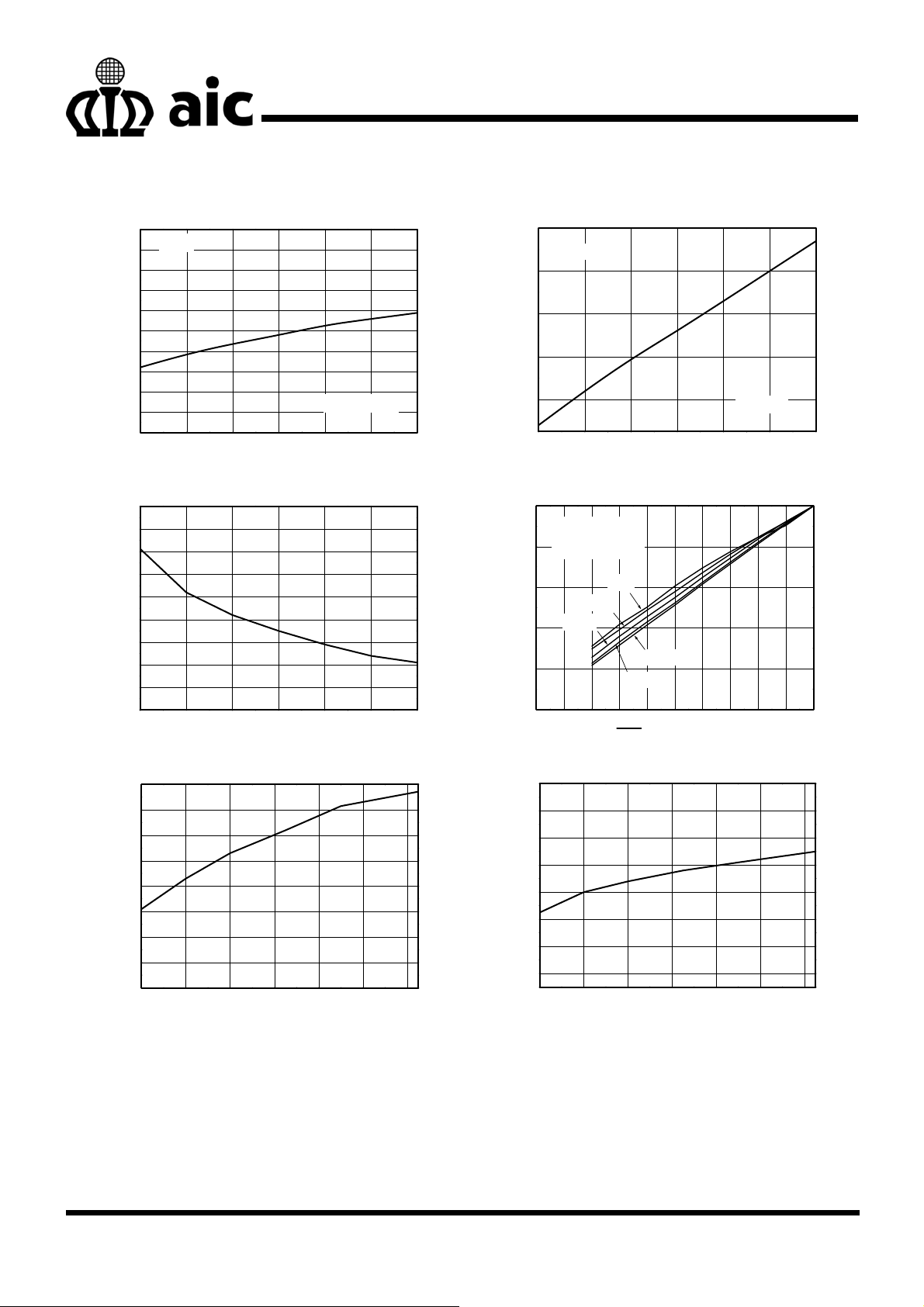
TYPICAL PERFORMANCE CHARACTERISTICS
200
FB=V
190
180
170
160
150
140
130
Supply Current (μA)
120
110
100
2.5 3.0 3.5 4.0 4.5 5.0 5.5
Fig. 2 Supply Current vs. Supply Voltage Fig. 3 Supply Current vs. Supply Voltage
IN
Non-Switching
Supply Voltage (V)
1600
FB=GND
1400
1200
1000
Supply Current (μA)
800
2.5 3.0 3.5 4.0 4.5 5.0 5.5
Supply Voltage (V)
Switching
1.7
1.6
1.5
1.4
1.3
(Ω)
1.2
DS-ON
R
1.1
1.0
0.9
0.8
2.53.03.54.04.55.05.5
Fig. 4 R
1.6
1.5
1.4
1.3
1.2
1.1
1.0
Switching Frequency (MHz)
0.9
0.8
-40-200 20406080
100
VIN=3.6V; L=6.8μH
C
=1μF; C
500Hz
=3.3μF
OUT
2kHz
1kHz
100Hz
200Hz
SHDN PIN PWM Duty (%)
Temperature (oC)
IN
80
3LEDs
60
(%)
LEDMAX
/I
40
LED_DUTY
I
20
0
0 102030405060708090100
Supply Voltage (V)
vs. Supply Voltage Fig. 5 Dimming Control by Shutdown Pin
DS_ON
Temperature (oC)
110
108
106
104
102
100
98
Feedback Voltage (mV)
96
-40-200 20406080
Fig. 6 Switching Frequency vs. Temperature Fig. 7 Feedback Voltage vs. Temperature
5
Page 6

AIC3643
TYPICAL PERFORMANCE CHARACTERISTICS (Continued)
24
23
22
LED Current (mA)
21
20
-40-200 20406080
VIN=4.2V
VIN=5.5V
VIN=3V
VIN=2.5V
Temperature (oC)
VIN=3.6V
V
, 2V/div
SHDN
I
, 200mA/div
INDUCTOR
V
, 2V/div
OUT
VIN=3V; 3LEDs; L=6.8μF; C
=3.3μF; I
OUT
LED
=20mA
Fig. 8 LED Current vs. Temperature Fig. 9 Start Up from Shutdown
V
, 5V/div
SW
, 200mA/div
I
INDUCTOR
Output Ripple, 50mV/div
VIN=3.6V; 3LEDs; L=6.8μF; C
OUT
=3.3μF; I
LED
=20mA
90
85
80
75
70
Efficiency (%)
65
60
0 5 10 15 20 25 30
VIN=4.2V
VIN=3.6V
VIN=3V
3 LEDs, 6.8μH
L1: GTSD31-6R8M, GOTREND
D1: SS0540, PAN JIT
Test Circuit refer to Fig.1
LED Current (mA)
Fig. 10 Operation Waveform Fig. 11 3LEDs Efficiency vs. LED Current
90
85
80
75
70
Efficiency (%)
65
60
0 5 10 15 20 25 30
VIN=4.2V
VIN=3V
4 LEDs, 6.8μH
L1: GTSD31-6R8M, GOTREND
D1: SS0540, PAN JIT
Test Circuit refer to Fig.1
LED Current (mA)
VIN=3.6V
90
85
VIN=4.2V
80
75
70
Efficiency (%)
65
60
0 5 10 15 20 25 30
VIN=3V
5 LEDs, 6.8μH
L1: GTSD31-6R8M, GOTREND
D1: SS0540, PAN JIT
Test Circuit refer to Fig.1
VIN=3.6V
LED Current (mA)
Fig. 12 4LEDs Efficiency vs. LED Current Fig. 13 5LEDs Efficiency vs. LED Current
6
Page 7

AIC3643
BLOCK DIAGRAM
OVP
100mV
VIN
FB
VREF
+
-
Error
AMP
28V
RC
CC
Over Voltage
Comparator
+
-
+
PWM
Comparator
Slope
Compensation
Current AMP.
PWM/PFM
Control
Control
Logic
1.2MHz
Oscillator
+
-
SHDN
SW
M1
Driver
RS
GND
PIN DESCRIPTIONS
PIN 1: SW - Switch pin. Connect
inductor/diode here. Minimize
trace area at this pin to reduce
EMI.
PIN 2: GND - Ground pin. Tie directly to local
ground plane.
PIN 3: FB - Feedback pin. Reference
voltage is 100mV. Connect
cathode of lowest LED and
resistor here. Calculate resistor
value to obtain LED current
according to the formula:
R
= 100mV/I
FB
LED
PIN 4:
SHDN
PIN 5: OVP - Overvoltage protection. When
PIN 6: VIN - Power input pin. Bypass VIN to
- Shutdown pin. Tie to higher than
1.5V to enable device, 0.3V or
less to disable device.
VOUT is greater than 28V, the
internal MOSFET turns off.
GND with a capacitor sitting as
close to VIN as possible.
7
Page 8

AIC3643
APPLICATION INFORMATION
Inductor Selection
A 6.8μH inductor is recommended for most
AIC3643 applications. Although small size and
high efficiency are major concerns, the inductor
should have low core losses at 1.2MHz and low
DCR (copper wire resistance). It is important to
ensure the inductor saturation current exceeding
the peak inductor current in application to prevent
core saturation. For CCM (Continuous Conduction
Mode) operation, the peak inductor current can be
calculated from:
DV
⋅
II
()
MAXINPEAK
=
+=
OSC
⋅
VI
OUT)MAX(LED
⋅η
V
+
)MIN(IN
)MAX()MIN(IN
Lf2
⋅×
DV
⋅
)MAX()MIN(IN
Lf2
⋅×
OSC
Capacitor Selection
The small size of ceramic capacitors makes them
ideal for AIC3643 applications. X5R and X7R
types are recommended because they retain their
capacitance over wider ranges of voltage and
temperature than other types, such as Y5V or
Z5U. 1
μF input capacitor with 3.3μF output
capacitor are sufficient for most AIC3643
applications.
Diode Selection
Schottky diodes, with their low forward voltage
drop and fast reverse recovery, are the ideal
choices for AIC3643 applications. The forward
voltage drop of an Schottky diode represents the
conduction losses in the diode, while the diode
capacitance (C
T or CD) r epresents the switching
losses. For diode selection, both forward voltage
drop and diode capacitance need to be
considered. In addition, the rating of selected
Schottky diode should be able to handle the
output voltage and the maximum peak diode
current.
LED Current Control
LED current is controlled by feedback resistor
(R
in Figure 1). The feedback reference voltage
FB
is 100mV. The LED current is 100mV/R
FB
. In
order to have accurate LED current, precision
resistors are preferred (1% recommended). The
formula for R
R =
FB
selection is shown below.
FB
mV100
I
LED
Open-Circuit Protection
In the cases of output open circuit, when the LEDs
are disconnected from the circuit or the LEDs fail,
the feedback voltage will be zero. AIC3643 will
then switch to a high duty cycle resulting in a high
output voltage, which may cause SW pin voltage
to exceed its maximum 33V rating. Connect builtin OVP (Over Voltage Protection) pin to output
terminal to prevent the damage resulting from an
open circuit condition.
Dimming Control
There are three different ways of dimming control
circuits as follows:
1. Using a PWM signal
PWM brightness control provides the widest
dimming range by pulsing the LEDs on and off at
full and zero current, respectively. The change of
average LED current depends on the duty cycle of
the PWM signal. Typically, a 0.1kHz to 2kHz
PWM signal is used. Two applications of PWM
dimming with AIC3643 are shown in Figure 14
and Figure 15. One, as Figure 14, uses PWM
signal to drive
control. The other, as Figure 15, employs PWM
signal going through a resistor to drive FB pin. If
the
SHDN pin is used, the increase of duty cycle
results in LED brightness enhancement. If the FB
pin is used, on the contrary, the increase of duty
cycle will decrease its brightness. In this
application, LEDs are dimmed by FB pin and
turned off completely by
2. Using a DC Voltage
For some applications, the preferred method of a
dimming control uses a variable DC voltage to
adjust LED current. The dimming control using a
DC voltage is shown in Figure 16. With a V
SHDN pin directly for dimming
SHDN.
DC
8
Page 9

μ
AIC3643
ranging from 0V to 5V, the selection of resistors in
Figure 16 results in dimming control of LED
current from 20mA to 0mA, respectively.
3. Using a Filtered PWM Signal
Filtered PWM signal can be considered as an
adjustable DC voltage. It can be used to replace
the variable DC voltage source in dimming
control. The circuit is shown in Figure 17.
Layout Consideration
In order to ensure a proper operation of AIC3643,
the following points should be managed
comprehensively.
1. The input capacitor and V
should be placed
IN
VIN
C1
1μF
PWM
6.8μH
VIN
SHDN
GND
AIC3643
L
SW
OVP
FB
as close as possible to each other to reduce
the input ripple voltage.
2. The output loop, which is consisted of the
inductor, the internal power switch, the
Schottky diode and the output capacitor,
should be kept as small as possible.
3. The routes with large current should be kept
short and wide.
4. Logically the large current on the converter
should flow at the same direction.
5. The FB pin should be connected to the
feedback resistors directly and the route
should be away from the noise sources.
D1
SS0540
C2
3.3μF
R
FB
5Ω
Fig. 14 Dimming Control with a PWM Signal
V
IN
C1
1μF
6.8
VIN
SHDN
GND
AIC3643
L
SW
OVP
FB
PWM
D1
SS0540
R2
49K
R1
1K
R
5Ω
C2
3.3μF
FB
Fig. 15 Dimming Control Using a PWM Signal
9
Page 10

μ
μ
Ω
Ω
AIC3643
V
IN
C1
1μF
L
6.8
H
SWVIN
OVPSHDN
D1
SS0540
C2
3.3
F
AIC3643
FB
V
DC
0~5V
R2
49K
R1
1K
R
5Ω
FB
GND
Fig. 16 Dimming Control Using a DC Voltage
VIN
C1
1μF
L
6.8μH
OVPSHDN
AIC3643
SWVIN
FBGND
PWM
Fig. 17Dimming Control Using a Filter PWM Signal
D1
SS0540
R3
5.1K
R2
49K
C3
0.1μF
R1
1K
C2
3.3μF
R
FB
5Ω
APPLICATION EXAMPLE
3.0~4.2V
C1
1μF
Fig. 18 Six White LEDs Application in Li-Ion Battery
L
6.8μH
VIN
SHDN
GND
AIC3643
SW
OVP
FB
D1
SS0540
C2
3.3μF
20mA
R
FB
5
R1
5
10
Page 11

AIC3643
PHYSICAL DIMENSIONS
SOT-23-6 PACKAGE OUTLINE DRAWING
AA
D
e
e1
(unit: mm)
E
E1
A
A2
A1
SEE VIEW B
b
WITH PLATING
c
BASE METAL
SECTION A-A
0.25
L1
VIEW B
L
θ
GAUGE PLANE
SEATING PLANE
Note : 1. Refer to JEDEC MO-178AB.
2. Dimension "D" does not include mold flash, protrusions
or gate burrs. Mold flash, protrusion or gate burrs shall not
exceed 10 mil per side.
3. Dimension "E1" does not include inter-lead flash or protrusions.
4. Controlling dimension is millimeter, converted inch
dimensions are not necessarily exact.
S
Y
M
B
O
L
A
A1
A2
b
c
D
E
E1
e
e1
L
L1
θ
MIN.
0.95
0.05
0.90
0.30
0.08
2.80
2.60
1.50
0.30
0°
SOT-23-6
MILLIMETERS
MAX.
1.45
0.15
1.30
0.50
0.22
3.00
3.00
1.70
0.95 BSC
1.90 BSC
0.60
0.42 REF
8°
11
Page 12

AIC3643
TSOT-23-6 PACKAGE OUTLINE DRAWING
D
E
E1
AA
e1
e
SEE VIEW B
b
WITH PLATING
A2
A
c
BASE METAL
SECTION A-A
A1
L
L1
VIEW B
Note : 1. Refer to JEDEC MO-193AA.
2. Dimension "D" does not include mold flash, protrusions
or gate burrs. Mold flash, protrusion or gate burrs shall not
exceed 6 mil per side.
3. Dimension "E1" does not include inter-lead flash or protrusions.
4. Controlling dimension is millimeter, converted inch
dimensions are not necessarily exact.
0.25
GAUGE PLANE
SEATING PLANE
θ
S
Y
M
B
O
L
A
A1
A2
b
c
D
E
E1
e
e1
L
L1
θ
MILLIMETERS
MIN.
-
0
0.70
0.30
0.08
2.80
2.60
1.50
0.30
0°
TSOT-23-6
MAX.
1.00
0.10
0.90
0.50
0.22
3.00
3.00
1.70
0.95 BSC
1.90 BSC
0.60
0.60 REF
8°
12
Page 13

AIC3643
Note:
Information provided by AIC is believed to be accurate and reliable. However, we cannot assume responsibility for use of any
circuitry other than circuitry entirely embodied in an AIC product; nor for any infringement of patents or other rights of third parties
that may result from its use. We reserve the right to change the circuitry and specifications without notice.
Life Support Policy: AIC does not authorize any AIC product for use in life support devices and/or systems. Life support devices or
systems are devices or systems which, (I) are intended for surgical implant into the body or (ii) support or sustain life, and whose
failure to perform, when properly used in accordance with instructions for use provided in the labeling, can be reaso nably expected
to result in a significant injury to the user.
13
Page 14

 Loading...