

Page 1
AIC1811
µ
µ
M1
BATTERY
One-Cell Lithium-Ion Battery Protection IC
n FEATURES
l Reduction in Board Size due to Miniature
Package SOT-23-5 and Less External
Components.
l Ultra-Low Quiescent Current at 7
l Ultra-Low Power-Down Current at 0.4
=2.3V).
l Precision Overcharge Protection Voltage
4.35V ± 50mV for the AIC1811A
4.30V ± 50mV for the AIC1811B
4.25V ± 50mV for the AIC1811C
l Built-in Delay Time Circuits for Overcharge,
Over-discharge, and Overcurrent Protection.
l Load Detection Function during Overcharge
Mode.
l Two Detection Levels for Overcurrent Protection.
A (VCC=3.5V).
A (V
CC
n DESCRIPTION
The AIC1811 battery protection IC is designed to
protect lithium-ion battery from damage or
degrading the lifetime due to overcharge,
overdischarge, and/or overcurrent for one-cell
lithium-ion battery powered systems, such as
cellular phones. The ultra-small package and less
required external components make it ideal to
integrate the AIC1811 into the limited space of
battery pack.
The accurate ±50mV overcharging detection
voltage ensures safe and full utilization charging.
Three different specification values for overcharge
protection voltage are provided for various
protection requirements. The very low standby
current drains little current from the cell while in
storage.
n APPLICATIONS
l Protection IC for One-Cell Lithium-Ion Battery
Pack.
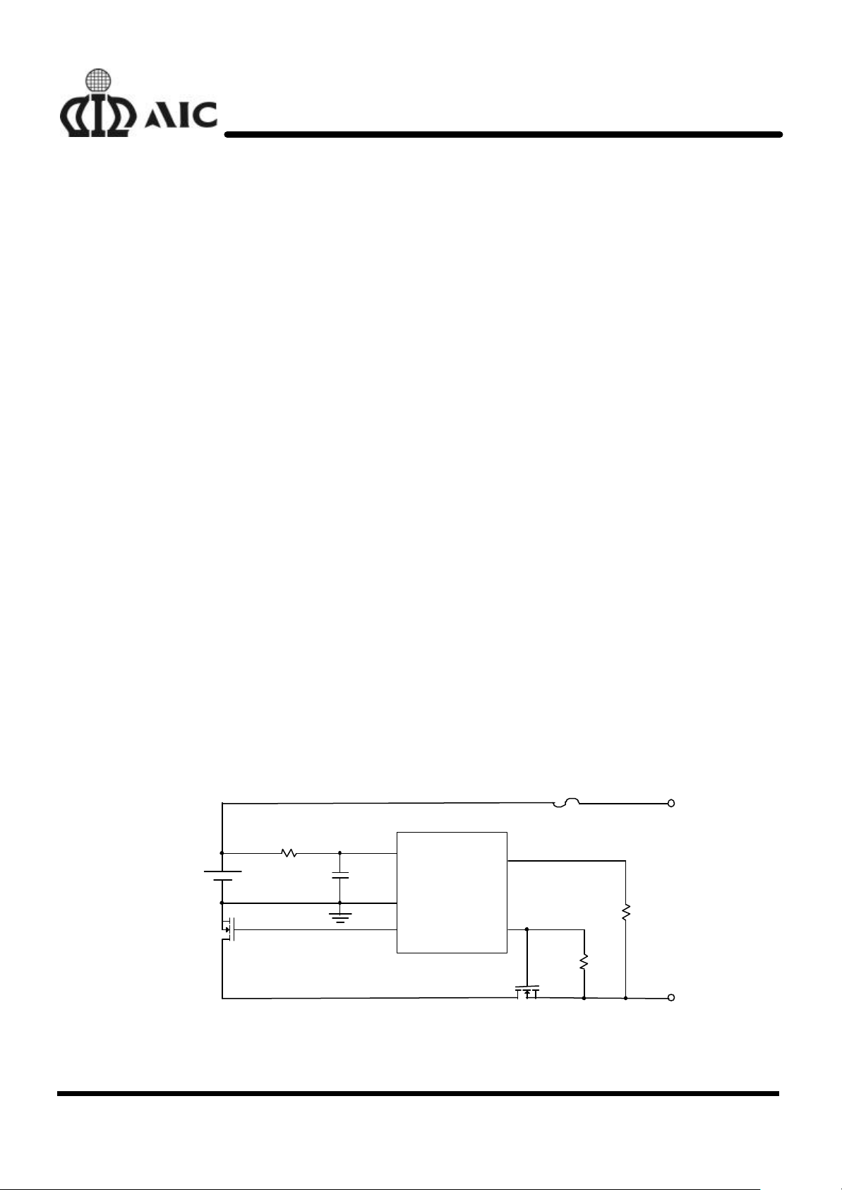
n TYPICAL APPLICATION CIRCUIT
R1
100
SI9926
Protection Circuit for One -Cell Lithium-Ion Battery
C1
0.1µF
5
VCC
2
GND
3
OD
AIC1811
CS
OC
4
1
M2 SI9926
BATT+
FUSE
R2
51K
R3
10M
BATT-
DS-1811-00 June 7, 00 www.analog.com.tw
1
Page 2
n ORDERING INFORMATION
V: SOT-2
OD
OC
AIC18
11
XC
X
4
5
AIC1811
ORDER NUMBER PIN CONFIGURATION
PACKAGE TYPE
3-5
AIC1811ACV
AIC1811BCV
TOP VIEW
AIC1811CCV
OVERCHARGE PROTECTION
(SOT-23-5)
A: 4.35V
B: 4.30V
C: 4.25V
n ABSOLUTE MAXIMUM RATINGS
Supply Voltage ....................................……………..................................................... 18V
DC Voltage Applied on other Pins ...............………………………….............................. 18V
Operating Temperature Range .....................................……………….............. -40°C~85°C
Storage Temperature Range .........................…………………..................... - 65°C~125°C
n TEST CIRCUIT
VCC
CS
321
GND
I
V
CC
R1
100
V
OD
CC
C1
0.1µF
5
VCC
2
GND
3
OD
AIC1811
CS
OC
4
1
R3
10M
R2
51K
S1
V
CS
V
OC
I
OC
2
Page 3
AIC1811
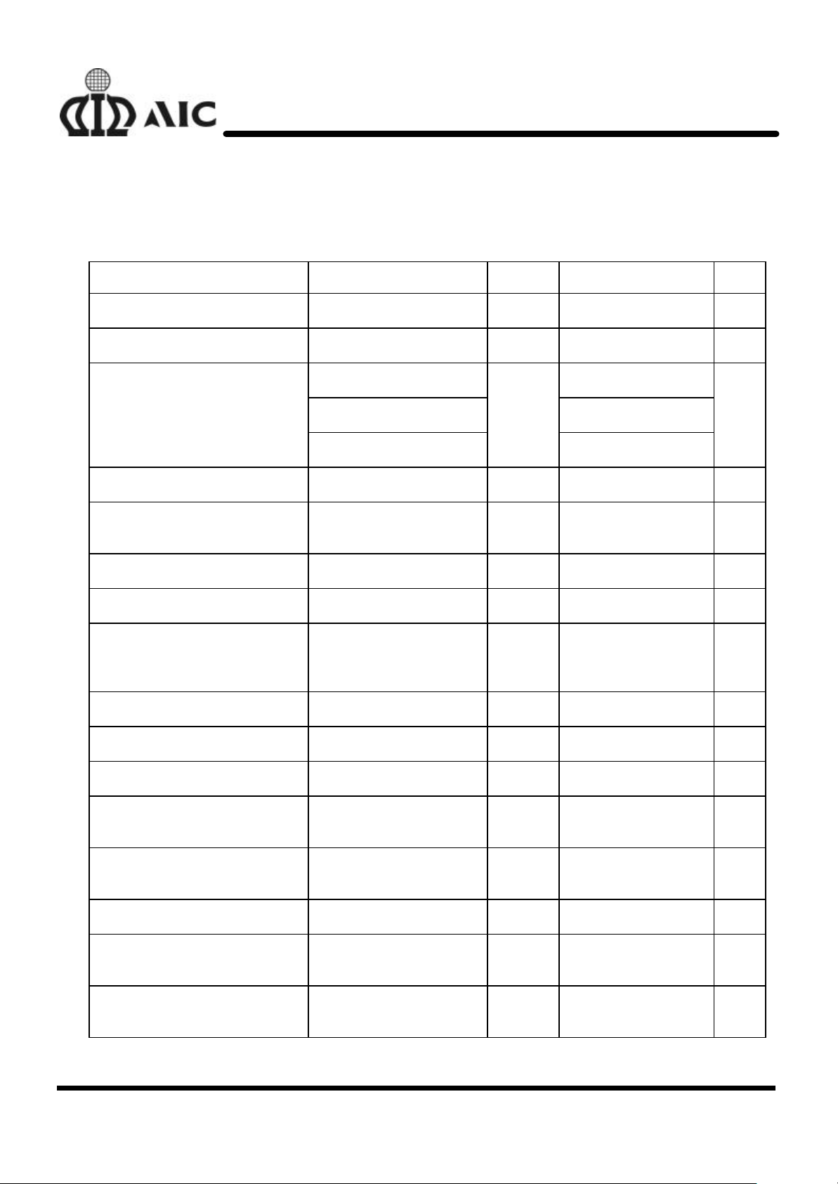
n ELECTRICAL CHARACTERISTICS (Ta=25 °C, unless otherwise specified.)
PARAMETER TEST CONDITIONS
SYMBOL
Supply Current VCC=3.5V I
Power-Down Current VCC=2.3V, I
Overcharge Protection Voltage
AIC1811A 4.30 4.35 4.40
AIC1811B 4.25 4.30 4.35
V
AIC1811C
Overcharge Hysteresis Voltage V
Overdischarge Protection
V
Voltage
Overdischarge Release Voltage V
Overcurrent Protection Voltage VCC=3.5V V
Overcharge Delay Time VCC=V
V
OCP
-0.1→
OCP
+ 0.1V
CC
PD
OCP
HYS
ODP
ODR
T
OIP
OC
MIN. TYP. MAX. UNIT
7 11 µA
0.4 1.0 µA
V
4.20 4.25 4.30
150 200 250 mV
2.2 2.4 2.6 V
2.6 2.9 3.2 V
180 200 220 mV
50 100 150 mS
Overdischarge Delay Time VCC= 2.5V →2.3V T
Overcurrent Delay Time (1) VCC=3.5V, 1V>VCS>0.2V T
Overcurrent Delay Time (2) VCC=3.5V, VCS>1V T
OC Pin Source Current VCC=3.5V, OC pin short to
GND
OD Pin Output “H” Voltage
V
OD Pin Output “L” Voltage V
Load Dectection Threshold
Voltage
Charge Detection Threshold
Voltage
VCC=V
–50mV V
OCP
VCC=2.3V V
I
OD
OI1
OI2
OC
DH
DL
LD
CH
50 100 150 mS
5 10 15 mS
150 300 450 µS
240 340 440 µA
VCC-0.1
VCC-
0.02
V
0.01 0.1 V
0.3 0.4 V
-0.45 -0.3 V
3
Page 4

n BLOCK DIAGRAM
Wake-up Control
Overcurrent
Enable
Enable
0.2V
OC
1.2V
1V
4
CS
5
VCC
-0.3V
0.3V
Delay Circuit
Load Detected
AIC1811
3
OD
GND
2
n PIN DESCRIPTIONS
PIN 1: OC - PMOS open drain output for
control of the charge control
MOSFET M2. In normal mode,
this PMOS turns on to pull the
gate of the MOSFET M2 to high,
then the MOSFET M2 turns on.
When overcharge occurs, this
PMOS turns off, then no current
flows through R3 and the
MOSFET M2 turns off.
PIN 2: GND - Ground pin. This pin is to be
connected to the negative terminal
of the battery cell.
PIN 3: OD - Output pin for control of the
discharge control MOSFET M1.
When overdischarge occurs, this
pin goes low to turn off the
Overdischarge
Delay Circuit
Overcharge
Delay Circuit
Power-down
Control
1
MOSFET M1 and discharging is
inhibited.
PIN 4: CS - Input pin for current sensing.
Using the sum of drain-source
voltages of the MOSFET M1 and
the MOSFET M2 (voltage
between CS and GND), it senses
discharge current during normal
mode and detects whether charge
current is present during powerdown mode. It also used to detect
whether load is connected during
overcharge mode.
PIN 5: VCC - Power supply pin. This pin is to be
connected to the positive terminal
of the battery cell.
4
Page 5

n APPLICATION INFORMATIONS
AIC1811
THE OPERATION
Overcharge Protection
When the voltage of the battery cell exceeds the
overcharge protection voltage (V
overcharge delay time (TOC) period, charging is
inhibited by the turning-off of the charge control
MOSFET M2. The overcharge delay time is fixed
to 100mS by IC internal circuit. The overcharge
condition is released in two cases:
1. The voltage of the battery cell becomes lower
than the overcharge release voltage (V
V
- V
OCP
) through self-discharge.
HYS
2. The voltage of the battery cell falls below the
overcharge protection voltage (V
load is connected.
When the battery voltage is above V
overcharge condition is never released even a
load is connected to the pack.
Overdischarge Protection
When the voltage of the battery cell goes below
the overdischarge protection voltage (V
beyond the overdischarge delay time (TOD) period,
discharging is inhibited by the turning-off of the
discharge control MOSFET M1. The
overdischarge delay time defaults to 100mS.
Inhibition of discharging is immediately released
when the voltage of the battery cell becomes
higher than overdischarge release voltage (V
through charging.
) beyond the
OCP
) and a
OCP
OCP
OCR
, the
ODR
or
ODP
overcurrent protection circuit operates and
discharging is inhibited by the turning-off of the
discharge control MOSFET M1. The overcurrent
condition returns to the normal mode when the
load is released and the impedance between the
BATT+ and BATT- terminals is 20MΩ or higher.
The AIC1811 is provided with the two overcurrent
detection levels (0.2V and 1V) and the two
overcurrent delay time (T
and T
OI1
OI2
)
corresponding to each overcurrent detection level.
Load Detection after Overcharge
The load detection function after overcharge is
implemented by detecting the CS pin voltage.
Once a load is connected to the battery pack after
overcharge, discharge current flows through the
parasitic diode of MOSFET M2 and there is a
diode voltage drop between CS and GND. Load is
determined to be connected to the pack if the CS
pin voltage is above load detection threshold
voltage (VLD).
)
Power-Down after Overdischarge
When overdischarge occurs, the AIC1811 will go
into power-down mode, turning off all the timing
generation and detection circuitry to reduce the
quiescent current to 0.4µA (VCC=2.3V). At the
same time, the CS pin is pull-high to VCC through
)
a high resistance resistor.
Overcurrent Protection
In normal mode, the AIC1811 continuously
monitors the discharge current by sensing the
voltage of CS pin. If the voltage of CS pin exceeds
the overcurrent protection voltage (V
) beyond
OIP
the overcurrent delay time (TOI) period, the
Charge Detection after Overdischarge
When overdischarge occurs, the discharge control
MOSFET M1 turns off and discharging is inhibited.
However, charging is still permitted through the
parasitic diode of M1. Once the charger is
connected to the battery pack, the AIC1811
immediately turns on all the timing generation and
5
Page 6

AIC1811
detection circuitry. Charging is determined to be in
progress if the voltage between CS and GND is
below charge detection threshold voltage (VCH).
DESIGN GUIDE
Selection of External Control MOSFETs
Because the overcurrent protection voltage is
preset, the threshold current for overcurrent
detection is determined by the turn-on resistance
of the discharge control MOSFET M1. The turn-on
resistance of the external control MOSFETs can
be determined by the equation: RON=V
(IT is the overcurrent threshold current). For
example, if the overcurrent threshold current IT is
designed to be 3A, the turn-on resistance of the
external control MOSFETs must be 33mΩ. Users
should be aware that turn-on resistance of the
MOSFET changes with temperature variation due
to heat dissipation. It changes with the voltage
between gate and source as well. (Turn-on
resistance of a MOSFET increases as the voltage
/ (2 x IT)
OIP
between gate and source decreases). Once the
turn-on resistance of the external MOSFET
changes, the overcurrent threshold current will
change accordingly.
Suppressing the Ripple and Disturbance
from Charger
To suppress the ripple and disturbance from
charger, connecting R1, C1 to VCC pin is
recommended.
Protection at CS pin
R2 is used for latch-up protection when charger is
connected under overdischarge condition and
overstress protection at reverse connecting of a
charger. Larger value of R2 reduces the charger
leakage current in overcharge mode, but possibly
disables the charge detection function after
overdischarge. Resistance of 51KΩ is
recommended.
6
Page 7

n TIMING DIAGRAM
VODV
V
l Overcharge and Overdischarge Protection
T
OC
V
OCP
V
OCP-VHYS
V
CC
V
OC
V
ODR
V
ODP
V
CC
Hi-Z
AIC1811
T
OC
T
OD
Hi-Z
V
V
OD
CC
0V
charger connected
l Overcurrent Protection (VCC=3.5V)
CC
V
1V
BATT-
0.2V
0V
VCC
0V
OI1
T
load connected
charger connected
<TOI1 TOI2
load connected
charger connected
CC
OC
V
7
Page 8

n PHYSICAL DIMENSIONS
e
D
A1
b
l SOT-25 (unit: mm)
AIC1811
H
E
A2
l SOT-23-5 MARKING
Part No. Marking
AIC1811ACV EA0A
AIC1811BCV EA0B
AIC1811CCV EA0C
C
L
θ
1
A
SYMBOL MIN MAX
A 1.00 1.30
A1 — 0.10
A2 0.70 0.90
b 0.35 0.50
C 0.10 0.25
D 2.70 3.10
E 1.40 1.80
e 1.90 (TYP)
H 2.60 3.00
L 0.37 —
θ1 1° 9°
8
 Loading...