

Page 1
AIC1721/1721D
3-pin Low Dropout Linear Regulator
Analog Integrations Corporation 4F, 9, Industry E. 9th Rd, Science Based Industrial Park, Hsinchu Taiwan, ROC www.analog.com.tw
DS-1721-01 TEL: 886-3-5772500 FAX: 886-3-5772510
1
FEATURES
Low Dropout Voltage of 130mV at 100mA Output
Current (5V Output Version).
Guaranteed 150mA/300mA Output Current.
Internal 1.3Ω P-MOSFET Draws no Base Current.
Low Ground Current at 55µA.
1% Accuracy Output Voltage of 3.3V/5V.
Input Voltage Range up to 12V (5V Output
Version).
Extremely Tight Load and Line Regulation.
Fast Transient Response.
Needs only 1µF for Stability.
Current and Thermal Limiting.
APPLICATIONS
Voltage Regulator for LAN Cards.
Wireless Communication Systems.
Battery Powered Systems.
DESCRIPTION
The AIC1721/1721D is the enhanced CMOS
version of the LP2950. The superior
characteristics of the AIC1721/1721D include
zero base current loss, very low dropout voltage,
and 1% accuracy output voltage. Typica-l ground
current remains approximately 55µA, from no
load to maximum loading conditions. Dropout
voltage at 100mA output current is significantly
lower than its bipolar counterpart: 130mV for the
AIC1721-5/1721D-5, and 180mV for the
AIC1721/ 1721D. Output current limiting and
thermal limiting are built in to provide maximal
protection to the AIC1721/ 1721D against fault
conditions.
While pin-to-pin compatible with the LP2950 and
the industry industry standard 78XX series of
voltage regulators, the AIC1721/1721D comes in
the popular3-pin SOT-89 or TO-92 packages.
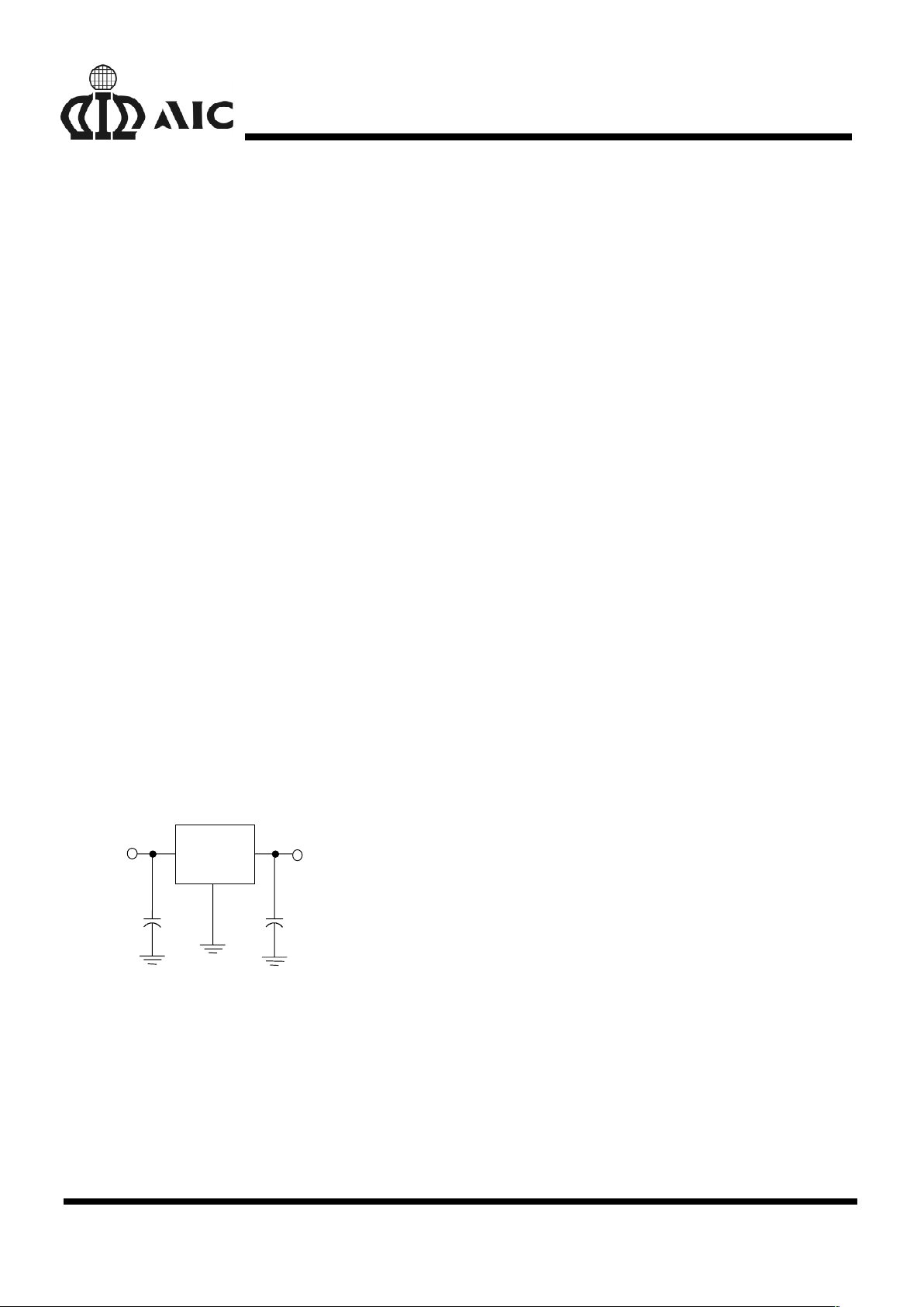
TYPICAL APPLICATION CIRCUIT
+
+
AIC1721
/
AIC1721D
10µF
C
OUT
V
OUT
VOUT
GND
VIN
1
µ
F
C
IN
V
IN
Negative Voltage Regulator
Page 2
AIC1721
2
ORDERING INFORMATION
ORDER NUMBER
AIC1721CX
AIC1721-5CX
AIC1721DCX
AIC1721D-5CX
(SOT-89)
AIC1721CZ
AIC1721-5CZ
AIC1721DCZ
AIC1721D-5CZ
(TO-92)
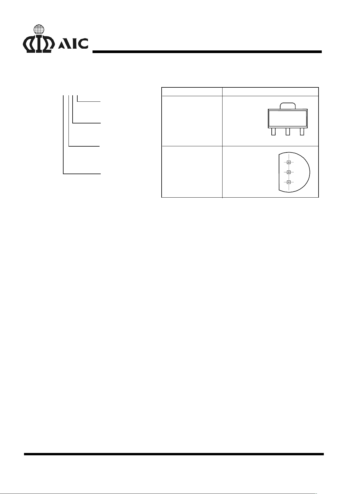
PIN CONFIGURATION
FRONT VIEW
1: VOUT
2: GND
3: VIN
AIC1721X-XXX
1
2
3
123
PACKAGING TYPE
X: SOT-89
Z: TO-92
TEMPERATURE RANGE
C: 0°C~+70°C
OUTPUT VOLTAGE
DEFAULT: 3.3V
5: 5.0V
OUTPUT CURRENT
DEFAULT: 150mA
D: 300mA
TOP VIEW
1: VOUT
2: GND
3: VIN
ABSOLUTE MAXIMUM RATINGS
Input Supply Voltage .................................…………......……................................ -0.3~12V
Operating Junction Temperature Range ..............….....……..….….............. -40°C~ 125°C
Storage Temperature Range ..............................….………........................ -65°C~150°C
Power Dissipation SOT-89 Package ..….…….…........... 0. 80W
TO-92 Package .......…….…............ 0.78W
TEST CIRCUIT
Refer to the TYPICAL APPLICATION CIRCUIT
Page 3

AIC1721
3
ELECTRICAL CHARACTERISTICS (Ta=25°
°°
°C, CIN=1µµµµF, C
OUT
=10µµµµF, unless
otherwise specified.)
PARAMETER TEST CONDITIONS MIN. TYP. MAX. UNIT
Output Voltage No Load
AIC1721/1721D-5
AIC1721/1721D
V
IN
=5.5~12V
V
IN
=3.6~12V
4.950
3.267
5.0
3.3
5.050
3.333
V
Output Voltage
Temperature
Coefficiency
(Note 1) 50
150 PPM/°C
Line Regulation IL=1mA
AIC1721/1721D-5
AIC1721/1721D
V
IN
=5.5~12V
V
IN
=3.6~12V
3
3
10
10
mV
Load Regulation
(Note 2)
AIC1721-5
AIC1721D-5
AIC1721
AIC1721D
V
IN
=7V, IL=0.1~150mA
V
IN
=7V, IL=0.1~300mA
V
IN
=5V, IL=0.1~150mA
V
IN
=5V, IL=0.1~300mA
7
7
7
7
15
25
15
25
mV
Current Limit
(Note 3)
AIC1721-5
AIC1721
AIC1721D-5
AIC1721D
V
IN
=7V, V
OUT
=0V
V
IN
=5V, V
OUT
=0V
V
IN
=7V, V
OUT
=0V
V
IN
=5V, V
OUT
=0V
320
320
320
320
440
440
440
440
mA
Dropout Voltage
(Note 4)
AIC1721/1721D
AIC1721-5
AIC1721
AIC1721D-5
AIC1721D
I
L
=0.1mA
I
L
=150mA
I
L
=150mA
I
L
=300mA
I
L
=300mA
0.2
200
270
400
540
10
300
370
500
640
mV
Ground Current IO=0.1mA~I
MAX
AIC1721/1721D-5
AIC1721/1721D
V
IN
=5.5~12V
V
IN
=4~12V
55
55
80
80
µA
Note 1: Guaranteed by design.
Note 2: Regulation is measured at constant junction temperature, using pulse testing with a low ON time.
Note 3: Current limit is measured by pulsing a short time.
Note 4: Dropout voltage is defined as the input to output differential at which the output voltage drops
100mV below the value measured with a 1V differential.
Page 4

AIC1721
4
BLOCK DIAGRAM
+
VOUT
VIN
GND
-
+
-
V
REF
TYPICAL PERFORMANCE CHARACTERISTICS
Output Voltage vs. Temperature
Normalized Out
p
ut Volt a
g
e
(
%
)
Temperature (°C)
50
100
98
99
100
101
102
0
-40
125
Ground Current vs. Input Voltage
Ground Current (
µ
A)
Input Voltage (V)
0
10
20
30
40
50
60
02468
10
12
Ground Current vs. Temperature
Ground Curr ent (
µ
A)
Temperature(°C)
125
02550
75 100
-25-50
50
52
54
56
58
60
IL=0.1mA
IL=150mA
IL=300mA
Dropout Voltage vs Load Current
Dropout Voltage (mV)
Load Current (mA
)
600
0
50
100 150
200
250
300
0
100
200
300
400
500
V
OUT
=3.3V
V
OUT
=5V
Page 5

AIC1721
5
TYPICAL PERFORMANCE CHARACTERISTICS (Continued)
Temper ature(°C)
Dropou t Voltage vs T emperature
Dropout Volt age(mV)
0 25 50 75 100 125-25-50
0
100
200
300
400
500
600
IL=0.1mA
V
OUT
=5V
IL=150mA
IL=300mA
Temperature (°C)
Short Circuit Current vs. Temperature
Short Circuit Current (mA)
02550
75 100 125
-25-50
200
300
400
500
AIC1721D
AIC1721
Line Transient Response
Time (mS)
Input Voltage
(V)
Output Voltage
(mV, AC)
0 0.1 0.2 0.3 0.4 0.5 0.6 0.7 0.8 0.9 1.0
100
50
0
-50
8
6
C
OUT
=1µF
I
L
=1mA
V
OUT
=5V
Load Transient Response
Load Current (mA) Output Voltage (mV)
150
0.1
100
0
-100
-200
0 0.5 1.0 1.5 2.0 2.5 3.0 3.5 4.0 4.5 5.0
C
OUT
=1µF
V
OUT
=5V
Load Transient Response
Time (mS)
Load Current
(mA)
Output Voltage
(mV, AC)
0 0.5 1.0 1.5 2.0 2.5 3.0 3.5 4.0 4.5 5.0
20
0
-20
150
0.1
C
OUT
=10µF
V
OUT
=5V
-40
-60
Page 6

AIC1721
6
PHYSICAL DIMENSIONS
SOT-89 (unit: mm)
SYMBOL MIN MAX
A 1.40 1.60
B 0.36 0.48
C 0.35 0.44
D 4.40 4.60
D1 1.62 1.83
E 2.29 2.60
e 1.50 (TYP.)
e1 3.00 (TYP.)
H 3.94 4.25
B
e
H
e1
D
D1
A
C
L
E
L 0.89 1.20
SOT89 Marking
Part No. Marking
AIC1714-30 AP30
AIC1714-33 AP33
AIC1714-50 AP50
TO-92 (unit: mm)
SYMBOL MIN MAX
A 4.32 5.33
C 0.38 (TYP.)
D 4.40 5.20
E 3.17 4.20
e1 1.27 (TYP.)
A
L
e1
D
C
E
L 12.7 -
 Loading...