

Page 1

AIC1567
5-bit DAC, Synchronous PWM Power Regulator
with Linear Controller
Analog Integrations Corporation 4F, 9, Industry E. 9th Rd, Science Based Industrial Park, Hsinchu Taiwan, ROC www.analog.com.tw
DS-1567-00 TEL: 886-3-5772500 FAX: 886-3-5772510
1
FEATURES
Switching Regulator and Low Dropout Linear
Regulator on single chip.
Simple Voltage-Mode PWM Control.
Dual N-Channel MOSFET Synchronous Drive.
Fast Transient Response.
±1.0% 5-Bit Digital-to-Analog Output Voltage.
Adjustable Current Limit Without External Sense
Resistor.
Full 0% to 100% Duty Ratio.
200KHz Free-Running Oscillator Programmable
up to 350KHz.
Power-Good Output Voltage Monitor.
Short Circuit Protection with Low Short Circuit
Output Current.
APPLICATIONS
Power Supply for Pentium II, Power PC and
Alpha Microprocessors.
High-Power 5V to 3.xV DC/DC Regulators.
Low-Voltage Distributed Power Supplies.
DESCRIPTION
The AIC1567 is a high power, high efficiency
switching regulator controller optimized for high
performance microprocessor applications. It is
designed to drive dual N-channel MOSFET in a
standard synchronous buck topology.
Featuring a low dropout linear regulator and a
digitally programmable switching regulator, the
AIC1567 includes monitoring and protection
capabilities in addition to all the essential
synchronous PWM control functions.
The internal 5-bit Digital-to-Analog Converter
(DAC) adjusts the output voltage from 2.0V to
3.5V in 0.1V increments and 1.3V to 2.0V in
0.05V increments. The precision reference and
voltage-mode control can provide output
regulation within ±1.0% over temperature and
line voltage shifts.
The internal oscillator of the AIC1567 free-runs
at 200KHz and can be adjusted up to 350KHz.
The resulting PWM duty ratio ranges from 0% to
100%. The error amplifier features a 11MHz
bandwidth and 6V/µS slew rate, which enables
high converter bandwidth for fast transient
response.
Page 2
AIC1567
2
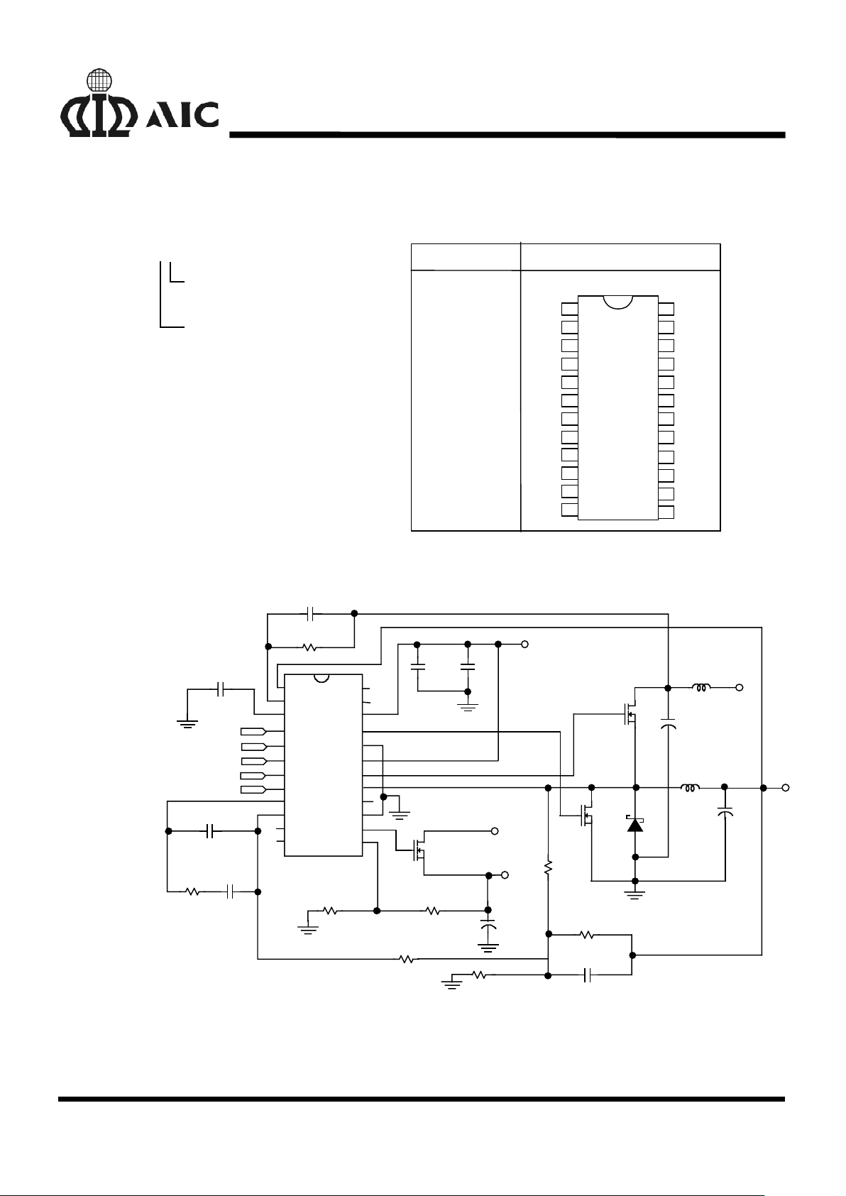
ORDERING INFORMATION
AIC1567 XX
PACKAGE TYPE
S: SMALL OUTLINE
TEMPERATURE RANGE
C: 0°C~70°C
PIN CONFIGURATION
ORDER NUMBER
AIC1567CS
(PLASTIC SO)
TOP VIEW
RT
OVP
VCC
LGATE
PGND
BOOT
UGATE
PHASE
PGOOD
GND
LIDRI
VLFB
24
23
22
21
20
19
18
17
1
2
3
4
5
6
7
8
VSEN
OCSET
SS
VID0
VID1
VID2
VID3
VID4
COMP
FB
CLP
CLN
9
10
11
12
16
15
14
13
TYPICAL APPLICATION CIRCUIT
VSEN RT
OCSET OVP
SS VCC
VID0 LGATE
VID1 PGND
VID2 BOOT
VID3 UGATE
VID4 PHASE
COMP PGOOD
FB GND
CLP LIDRI
CLN VLFB
C2
0.1
µ
F
C1
1
µ
F
C5
1000pF
C7
33pF
C6
1000pF
0.1µF
+
C1
1000
µ
F
5V
137
1%
R3
47K
R5
3.01K
Ω
R6
90.9K
R2
2.2K
C8
R1
237
1%
R7
+
1000µF
x 8
R4
15K
D1
1N5820
M2
NDP603AL
VID0
VID1
VID2
VID3
VID4
V
CORE
V
I/O
3.3V
10A
12V
AIC1567
M3
FD3055
0.1µF
R8
1.2M
C3
1000µF x 3
3µH
L2
M1
RFP45N03L
+
L1
1
µ
H
5V
C4
Pentium
II V
CORE
and V
I/O
DC/DC Converter
Page 3
AIC1567
3
ABSOLUTE MAXIMUM RATINGS
Supply Voltage, VCC....…..................................……………........................................... 15V
Boot Voltage, V
BOOT
………...................……………...................................................... 15V
Input, Output, or I/O Voltage .....…….........……………......…....... GND - 0.3V to VCC+0.3V
ESD Classification ...........................…………......................……......................... Class 2
Recommended Operating Conditions
Supply Voltage, VCC....…...................…………………..........................…….......... 12V±10%
Ambient Temperature Range ....……………………............................................ 0°C ~ 70°C
Junction Temperature Range ....…………………….......................................... 0°C ~100°C
Thermal Information
Thermal Resistance, θJA (Typical, Note 1)
SOIC Package .....................…….........……………………………….........…. 100°C/W
SOIC Package (with 3 in
2
of Copper) …………………………………......….. 90°C/W
Maximum Junction Temperature (Plastic Package) ….……………….…................... 150°C
Maximum Storage Temperature Range ……………………..……......…......... -65°C~150°C
Maximum Lead Temperature (Soldering 10 sec) …………………………......…......... 300°C
Note 1: symbol
θ
JA
is measured with the component mounted on an evaluation PC board in free air.
TEST CIRCUIT
Refer to TYPICAL APPLICATION CIRCUIT.
ELECTRICAL CHARACTERISTICS (VCC= 12V, Ta=25°
°°
°C, unless otherwise
specified.)
PARAMETER TEST CONDITIONS SYMBOL MIN. TYP. MAX. UNIT
VCC Supply Current
Nominal Supply UGATE Open I
VCC
2mA
Power-On Reset
VCC Threshold V
OCSET
=4.5V 7 8.5 V
Rising V
OCSET
Threshold 1.26 V
Oscillator
Free Running Frequency RT Open 170 200 230 KHz
Total Variation 6KΩ< RT<200KΩ -20 +20 %
Ramp Amplitude RT Open ∆V
OSC
1.5 V
P-P
Page 4

AIC1567
4
ELECTRICAL CHARACTERISTICS (Continued)
PARAMETER TEST CONDITIONS SYMBOL MIN. TYP. MAX. UNIT
Reference and DAC
DACOUT Voltage Accuracy V
DAC
=1.8V ~3.5V -1.0 +1.0 %
Error Amplifier
DC Gain 76 dB
Gain-Bandwidth Product GBW 11 MHz
Slew Rate SR 6 V/µS
Gate Driver
Upper Gate Source R
UGATE
8.0 12 Ω
Upper Gate Sink R
UGATE
5.5 10 Ω
Lower Gate Source R
LGATE
8.0 12 Ω
Lower Gate Sink R
LGATE
5.5 10 Ω
Protection
Over-Voltage Trip (V
SEN/DACOUT
) 106 115 125 %
OCSET Current Source
V
OCSET
=4.5VDC I
OCSET
170 200 230 µA
OVP Sourcing Current
V
VSEN
=5.5V, V
OVP
=0V I
OVP
30 mA
Soft Start Current I
SS
10 µA
Soft Start Sink Current under
Current Limit
V
VSEN
=V
DAC
, V
OCSET
=5.0V,
V
PHASE
=0V,
V
FB
=VDAC=50mV
130 µA
Soft Start Sink Current under
Hard Current Limit
V
VSEN
=0, V
OCSET
=5.0V,
V
PHASE
=0V, VFB=0V
65 mA
Power Good
Upper Threshold (V
VSEN
/V
DAC
)V
VSEN
Rising 106 114 %
Lower Threshold (V
VSEN
/ V
DAC )VVSEN
Falling 84 94 %
Hysteresis (V
VSEN
/ V
DAC
) Upper and Lower Threshold 2 %
PGOOD Voltage Low I
PGOOD
=5mA V
PGOOD
0.5 V
Linear Regulator
VLFB Feedback Voltage 1.18 1.21 1.24 V
VLFB Bias Current 40 nA
LIDRI Sourcing Current 10 mA
Current Limiting Threshold 10 20 30 mV
Page 5

AIC1567
5
BLOCK DIAGRAM
PWM
COMPARATOR
CURRENT SENSE
LINEAR AMP.
ERROR
AMP
CLN
VDAC
1.2V
CLP
COMP
FB
VLFB
LIDRI
OSCILLATOR
REFERENCE
5BITS
DAC
RT
PHASE
OVER
CURRENT
VSEN
OCSET
SOFT
START
200µA
CONTROL
LOGIC
OVP
POW ER-ON
RESET
VCC
50%
POW ER
GOOD
90%
PGOOD
110%
115%
+
-
VID0
VID3
VID2
VID1
GND
BOOT
UGATE
10µA
4V
SS
+
-
+
-
+
-
+
-
+
+
-
+
-
+
-
+
-
+
-
20m
V
VID4
PGND
LGATE
OVP
VCC
Page 6

AIC1567
6
PIN DESCRIPTIONS
PIN 1: VSEN - Converter output voltage sense
pin. Connect this pin to the
converter output. The PGOOD
and OVP comparator circuits use
this signal to report output
voltage status and for
overvoltage protection function.
PIN 2: OCSET - Current limit sense pin. Connect
a resistor R
OCSET
from this pin to
the drain of the external
MOSFET. R
OCSET
, an internal
200µA current source (I
OCS
), and
the external MOSFET onresistance (R
DS(ON)
) jointly set
the over current trip point
according to the following
equation:
I
IR
R
PEA K
OCS OCSET
DS ON
=
×
()
If FB pin voltage is sensed to be
below 50% of the internal
voltage reference VDAC, the
over current comparator cycles
the soft-start function.
PIN 3: SS - Soft start pin. Connect a
capacitor from this pin to ground.
An internal 10µA current source
provides soft start function for
the converter.
PIN 4: VID0
PIN 5: VID1
PIN 6: VID2
PIN 7: VID3
PIN 8: VID4 - 5-bit DAC voltage select pin. TTL
inputs used to set the internal
voltage reference VDAC. When
left open, these pins are
internally pulled up to 5V and
provide logic ones. The level of
VDAC sets the converter output
voltage as well as the PGOOD
and OVP thresholds.
Table 1 specifies the VDAC
voltage for the 32 combinations
of DAC inputs.
PIN 9: COMP - External compensation pin. This
pin is connected to error
amplifier output and PWM
comparator. An RC network is
connected to FB pin to
compensate the voltage-control
feedback loop of the converter.
PIN 10: FB - The error amplifier inverting
input pin. The FB pin and COMP
pin are used to compensate the
voltage-control feedback loop.
PIN 11: CLP - Linear regulator current sense
pin. This pin is the positive input
of the current sense comparator.
PIN 12: CLN - Linear regulator current sense
pin. This pin is the negative input
of the current sense comparator.
PIN 13: VLFB - Negative feedback pin for the
linear regulator error amplifier.
PIN 14: LIDRI - Linear regulator output drive pin.
This pin can drive either a
Darlington NPN or an N-channel
MOSFET.
PIN 15: GND - Signal GND. It also serves as
the power GND for the upper
gate driver.
PIN 16: PGOOD-Power good indicator pin.
PGOOD is an open drain output.
This pin is pulled low when the
converter output is ±10% out of
the VDAC reference voltage.
Table 1. Output Voltage Program
VID4 VID3 VID2 VID1 VID0 VDAC
100003.5V
100013.4V
100103.3V
100113.2V
101003.1V
101013.0V
101102.9V
101112.8V
110002.7V
110012.6V
110102.5V
110112.4V
111002.3V
111012.2V
Page 7

AIC1567
7
111102.1V
111112.0V
000002.05V
000012.00V
000101.95V
000111.90V
001001.85V
001011.80V
001101.75V
001111.70V
010001.65V
010011.60V
010101.55V
010111.50V
011001.45V
011011.40V
011101.35V
011111.30V
PIN 17: PHASE - Over current detection pin. Connect
the PHASE pin to source of the
external MOSFET. This pin detects
the voltage drop across the MOSFET
R
DS(ON)
for over-current protection.
PIN 18: UGATE- External MOSFET gate drive pin.
Connect UGATE to gate of the
external MOSFET.
PIN 19: BOOT - External MOSFET driver power
supply pin. To convert 5V main power
to V
CORE
power by driving N-channel
MOSFET, supply voltage of no higher
than 12V is recommended since the
negative power terminal of the
internal driver is internally tied to
GND.
PIN 20: PGND - Driver power GND pin. PGND should
be connected to a low impedance
ground plane in close to lower NMOSFET source.
PIN 21: LGATE - Lower N-MOSFET gate driver pin.
PIN 22: VCC - The chip power supply pin. It also
serves as power supply for LGATE
driver. Recommended supply voltage
is 12V.
PIN 23: OVP -Over voltage indicator pin. This pin
also provides a driver source current
to turn on an external SCR in the
event of an over voltage condition.
PIN 24: RT - Frequency adjustment pin.
Connecting a resistor (RT) from this
pin to GND, increase the frequency
by the following equation.
FKHzST≅+
×
200
510
5
log R
PHYSICAL DIMENSIONS
24 LEAD PLASTIC SO (300 mil) (unit: mm)
SYMBOL MIN MAX
A 2.35 2.65
A1 0.10 0.30
B 0.33 0.51
C 0.23 0.32
D 15.20 15.60
E 7.40 7.60
e 1.27(TYP)
H 10.00 10.65
e
B
D
A
A
1
C
E
H
L
L 0.40 1.27
 Loading...