

Page 1

AIC1341
High Performance, Triple-Output, Auto-
Tracking Com bo Controller
Analog Integrations Corporation 4F, 9, Industry E. 9th Rd, Science Based Industrial Park, Hsinchu Taiwan, ROC
www.analog.com.tw
DS-1341-00 May 24, 01 TEL: 886-3-5772500 FAX: 886-3-5772510 1
n
FEATURES
l Provide Triple Accurate Regulated Voltages
l Optimized Voltage-Mode PWM Control
l Dual N-Channel MOSFET Synchronous Drivers
l Fast Transient Response
l Adjustable Over Current Protection using R
DS(ON)
.
No External Current Sense Resistor Required.
l Programmable Softstart Function
l 200KHz Free-Running Oscillator
l Robust Output s Auto-Tracking Characteristics
l Sink and Source Capabilities with External Circuit
n
APPLICATIONS
l Advanced PC Mboards
l Information PCs
l Servers and Workstations
l Internet Appliances
l PC Add-On Cards
l DDR Termination
n
GENERAL DESCRIPTION
The AIC1341 combines a synchronous voltage
mode PWM controller with two linear controllers
as well as the monitoring and protection functions
in this chip. The PWM controller regulates the
output voltage with a synchronous rectified stepdown converter. The built-in N-Channel MOSFET
drivers also help to simplify the design of stepdown converter. It is able to power CPUs, GPUs,
memories, chipset s and multi-voltage applications.
The PWM controller features over current protection using R
DS(ON)
. It improves efficiency and saves
cost, as there is no expensive current sense resistor required.
Two built-in adjustable linear controllers drive an
external MOSFETs to form two linear regulators
that regulates power for multiple system I/O. Output voltage of both linear regulators can also be
adjusted by means of the external resistor divider.
Both linear regulators feature current limit. For a
system I/O requires current less than 500mA, the
AIC1340 is recommended for saving one external
MOSFET.
The programmable soft-start design provodes a
controlled output voltage rise, which limits the current rate during power on time.
The shutdown function is also provided for disabling the combo controller.
Page 2
AIC1341
2
n
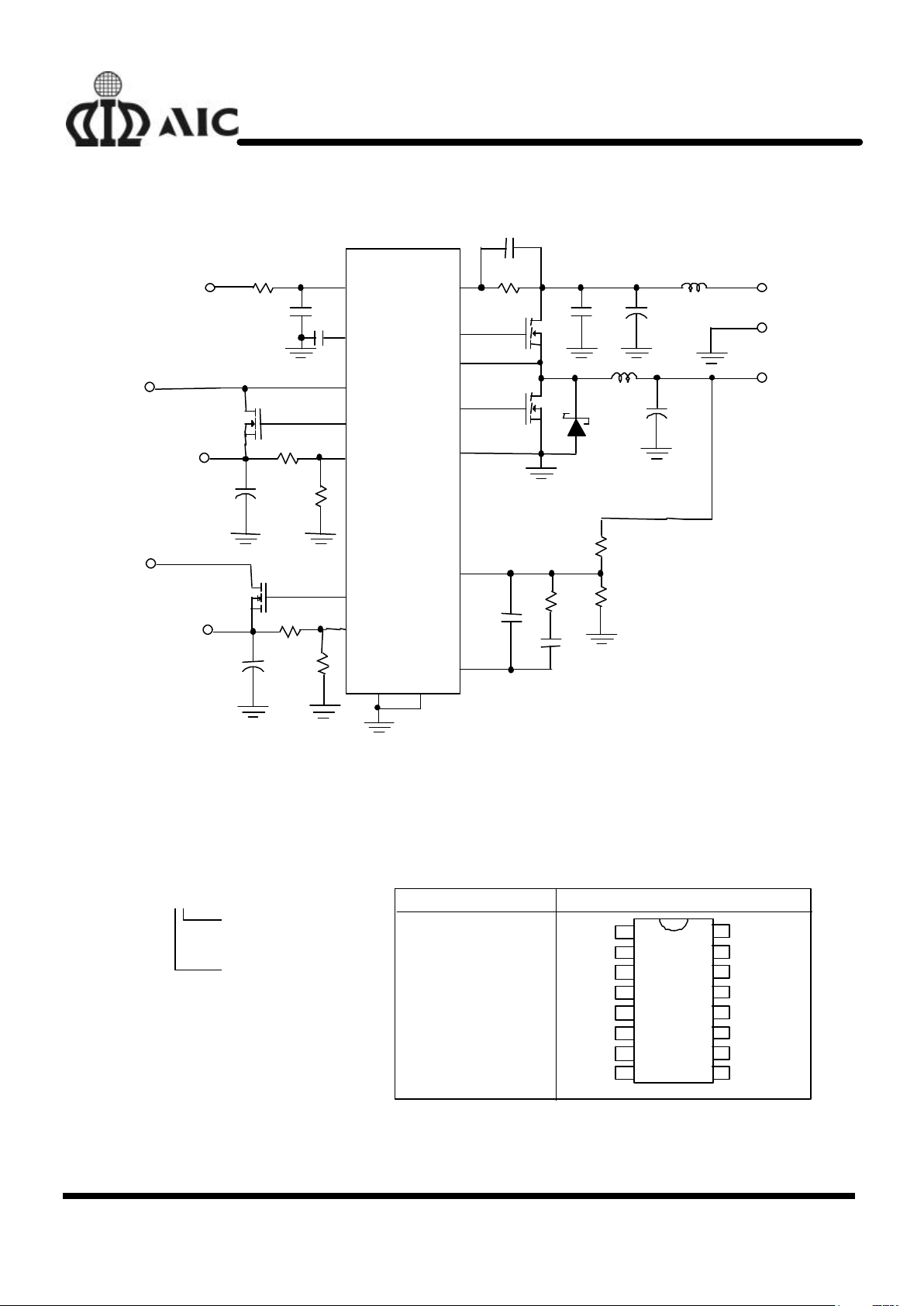
TYPICAL APPLICATION CIRCUIT
+
+
UGATE
PHASE
VIN2
LGATE
GATE3
PGNDFB3
GATE2
FB2
COMP1
SS
GND
+5VIN
VCC
+12VIN
15
OCSET
4
7
11
8
6
VOUT2
VOUT3
+3.3VIN
12
13
16
1
2
14
14
VOUT1
+
5
GND
FB1
3
SD
10
+
+3.3VIN
AIC1341CS
Q1
Q2
Typical Triple-Output Application
n
ORDERING INFORMATION
ORDER NUMBER
PIN CONFIGURATIONAIC1341-XX
AIC1341CS
(SO 16)
PACKAGING TYPE
S: SMALL OUTLINE
TEMPERATURE RANGE
C: O°C~+70°C
1
3
4
2
5
7
68FB2
UGATE
SD
VCC
PHASE
SS
VIN2
GATE2
OCSET
LGATE
PGND
FB3
FB1
COMP1
GATE3
GND
16
14
15
13
12
11
9
10
Page 3
AIC1341
3
n
ABSOLUTE MAXIMUM RATING
Absolute Maximum Ratings
Supply Voltage (VCC) .............................................................................................................. 15V
UGATE....................................................................................................GND - 0.3V to VCC + 0.3V
LGATE ....................................................................................................GND - 0.3V to VCC + 0.3V
Input Output and I/O Voltage .................................................................................GND - 0.3V to 7V
Operating Conditions
Ambient Temperature Range ........................................................................................0° C to 85°C
Maximum Operating Junction Temperature ............................................................................. 100°C
Supply Voltage, VCC .......................................................................................................15V±10%
Thermal Information
Thermal Resistance θJA (°C/W)
SOIC Package.......................................................................................................100°C/W
Maximum Junction Temperature (Plastic Package).................................................................. 150°C
Maximum Storage Temperature Range .......................................................................-65°C to 150°C
Maximum Lead Temperature (Soldering 10s)........................................................................... 300°C
n
TEST CIRCUIT
Refer to APPLICATION CIRCUIT.
n
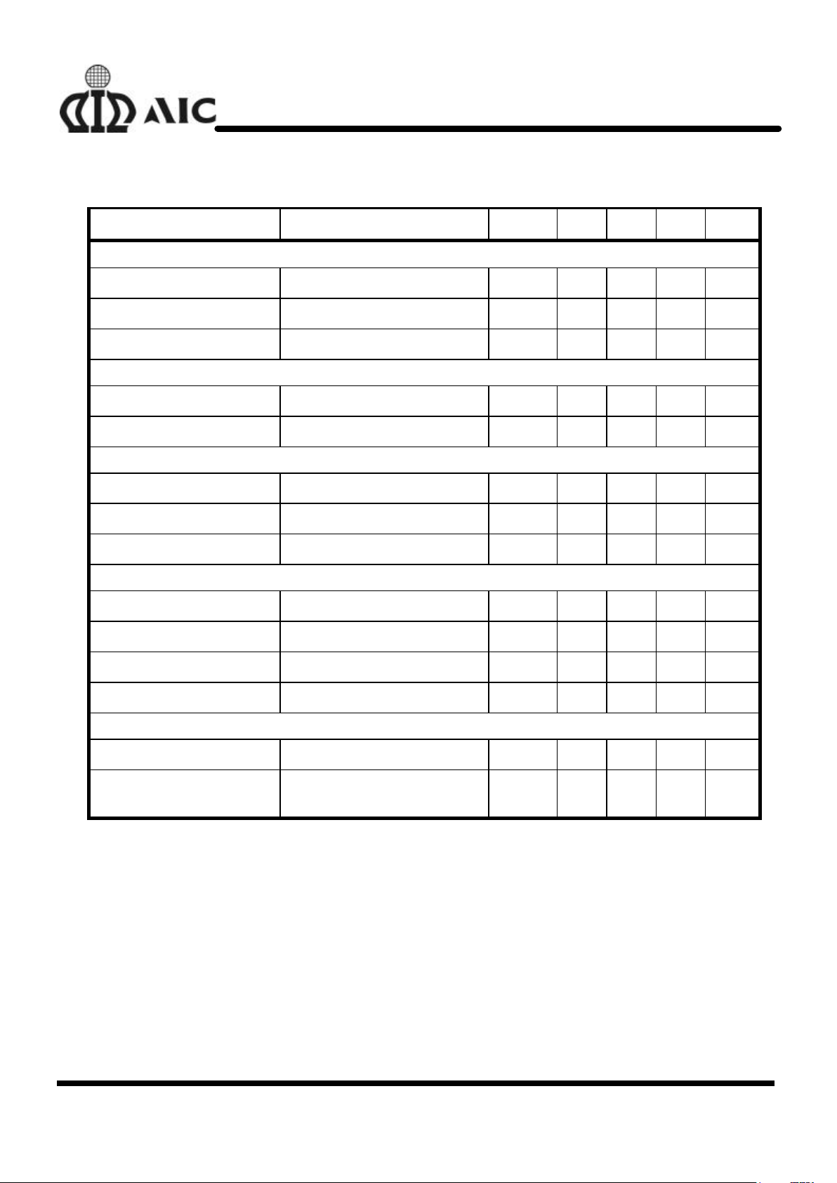
ELECTRICAL CHARACTERISTICS
(Vcc=12V, TJ=25°C, Unless otherwise
specified)
PARAMETER TEST CONDITIONS SYMBOL MIN. TYP. MAX. UNIT
VCC SUPPLY CURRENT
Supply Current UGATE, LGATE, GATE2 and
GATE3 open
I
CC
1.8 5 mA
POWER ON RESET
Rising VCC Threshold V
OCSET
=4.5V VCC
THR
8.6 9.5 10.4 V
Falling VCC Threshold V
OCSET
=4.5V VCC
THF
8.2 9.2 10.2 V
Rising VIN2 Under-Voltage
Threshold
VIN2
THR
2.5 2.6 2.7 V
VIN2 Under-Voltage Hysteresis
VIN2
HYS
130 mV
Rising V
OCSET1
Threshold V
OCSETH
1.3 V
Page 4
AIC1341
4
n
ELECTRICAL CHARACTERISTICS
(Continued)
PARAMETER TEST CONDITIONS
SYMBOL
MIN. TYP. MAX. UNIT
OSCILLATOR and REFERENCE
Free Running Frequency F 170 200 230 KHz
FB2 Reference Voltage V
REF2
1.245 1.270 1.295 V
FB3 Reference Voltage V
REF3
1.250 1.275 1.300 V
LINEAR CONTROLLER
Regulation 0 < I
GATE2/3
< 10mA -2.5 +2.5 %
Under-Voltage Level FB2/3 falling FB2/3
UV
70 80 %
PWM CONTROLLER ERROR AMPLIFIER
DC GAIN 76 dB
Gain Bandwidth Product GBWP 11 MHz
Slew Rate COMP1=10pF SR 6 V/µS
PWM CONTROLLER GATE DRIVER
Upper Drive Source VCC=12V, V
UGATE
=11V R
UGH
5.2 6.5 Ω
Upper Drive Sink VCC=12V, V
UGATE
=1V R
UGL
3.3 5 Ω
Lower Drive Source VCC=12V, V
LGATE
=11V R
LGH
4.1 6 Ω
Lower Drive Sink VCC=12V, V
LGATE
=1V R
LGL
3 5 Ω
PROTECTION
Soft-Start Current I
SS
11 µA
Chip Shutdown Soft Start
Threshold
1.0 V
Page 5

AIC1341
5
n
PIN DESCRIPTIONS
Pin 1: PHASE: Over-current detection pin. Con-
nect the PHASE pin to source of
the external high-side NMOSFET. This pin detects the
voltage drop across the high-side
N-MOSFET R
DS(ON)
for over-
current protection.
Pin 2: UGATE: External high-side N-MOSFET
gate drive pin. Connect UGATE
to gate of the external high-side
N-MOSFET.
Pin 3: SD: To shut down the system, active
high or floating. If connecting a
resistor to ground, keep the re-
sistor less than 4.7K Ω
Pin 4: VCC: The chip power supply pin. It also
provides the gate bias charge for
all the MOSFETs controlled by
the IC. Recommended supply
voltage is 12V.
Pin 5: SS: Soft-start pin. Connect a capaci-
tor from this pin to ground. This
capacitor, along with an internal
10µA (typically) current source,
sets the soft-start interval of the
converter.
Pulling this pin low will shut down
the IC.
Pin 6: FB2: Connect this pin to a resistor di-
vider to set the linear regulator
output voltage.
Pin 7: VIN2: This pin supplies power to the
internal regulator. Connect this
pin to a suitable 3.3V source.
Additionally, this pin is used to
monitor the 3.3V supply. If, following a start-up cycle, the voltage drops below 2.6V (typically),
the chip shuts down. A new softstart cycle is initiated upon re-
turn of the 3.3V supply above
the under-voltage thres hold.
Pin 8: GATE2: Linear Controller output drive pin.
This pin can drive either a Darlington NPN transistor or a Nchannel MOSFET.
Pin 9: GND: Signal GND for IC. All voltage
levels are measured with respect
to this pin.
Pin 10: GATE3: Linear Controller output drive pin.
This pin can drive either a Darlington NPN transistor or an Nchannel MOSFET.
Pin 11: FB3 Negative feedback pin for the
linear controller error amplifier
connect this pin to a resistor divider to set the linear controller
output voltage.
Pin 12: COMP1 External compensation pin. This
pin is connected to error amplifier output and PWM comparator.
A RC network is connected to
FB1 to compensate the voltage
control feedback loop of the converter.
Pin 13: FB1 The error amplifier inverting input
pin. The FB1 pin and COMP1 pin
are used to compensate the voltage-control feedback loop.
Pin 14: OCSET: Current limit sense pin. Connect
a resistor R
OCSET
from this pin to
the drain of the external high-side
N-MOSFET. R
OCSET
, an internal
200µA current source (I
OCSET
),
and the upper N-MOSFET onresistance (R
DS(ON)
) set the overcurrent trip point according to the
following equation:
I
I R
R
PEAK
OCSET OCSET
DS(ON)
=
×
Page 6

AIC1341
6
Pin 15: PGND: Driver power GND pin. PGND
should be connected to a low
impedance ground plane in close
to lower N-MOSFET source.
Pin 16: LGATE: Lower N-MOSFET gate drive pin.
n
TYPICAL PERFORMANCE CHARACTERISTICS
U
GATE
L
GATE
U
GATE
L
GATE
Fig.1 The gate drive waveforms
FAULT
SS
10A/div
Inductor Current
Over Load
Applied
VOUT1=3.5V
VOUT1=1.3V
V
OUT1
=2V
SS
Fig.2 Over-Current Operation on Inductor Fig.3 Soft start initiates PWM Output
Page 7

AIC1341
7
n
TYPICAL PERFORMANCE CHARACTERISTICS (Continued)
V
OUT1
5A to 12A Load Step
2.0V
DC
V
OUT3 (
2mV/div
)
1A to 2A Load Step
Fig.4 Transient Response of PWM Output Fig.5 Transient Response of Linear Controller
n
BLOCK DIAGRAM
+
+
++
+
+
+
+
+
+
SSSS
POR
5V
-
+
3.6V
QRS
QRS
-
+0.2V
5V
SD
POR
2.6V
COUNT 3
VIN2
VCC
1.3V
200uA
9.5V
FB2
GATE2
OCSET
COMP1
R
R
QS
1.3V
FB3
OSCILLATOR
GATE CONTROL
SS
SLOW DISCHARGE
FAST DISCHARGE
20uA
10uA
ERROR AMP
PWM COMP
200KHz
70K
4V
SS
INHIBIT
LUV
OC1
LUV
OC1
PHASE
UGATE
VCC
PGND
LGATE
VCC
0.3V
1.26V
FB1
GATE3
GND
Page 8

AIC1341
8
n
DESCRIPTION
The AIC1341 is designed for applications with
multiple voltage demand. This IC has one PWM
controller and two linear controllers. The PWM
controller is designed to regulate the voltage
(V
OUT1
) by driving 2 MOSFETs (By U
GATE
and
L
GATE
) in a synchronous rectified buck converter
configuration. The voltage is regulated to a level,
which is decided by a resistor devide network.
The Power-On Reset (POR) function continually
monitors the input supply voltage +12V at VCC
pin, the 5V input voltage at OCSET pin, and the
3.3V input at VIN2 pin. The POR function initiates
soft-start operation after all three input supply
voltage exceeds their POR thresholds.
Soft-Start
The POR function initiates the soft-start sequence.
Initially, the voltage on SS pin rapidly increases to
approximate 1V. Then an internal 10µA current
source charges an external capacitor (CSS) on the
SS pin to 4V. As the SS pin voltage slews from
1V to 4V, the PWM error amplifier reference input
(Non-inverting terminal) and output (COMP1 pin) is
clamped to a level proportional to the SS pin voltage. As the SS pin voltage slew from 1V to 4V,
the output clamp generates PHASE pulses of increasing width that charge the output capacitors.
Additionally both linear regulator’s reference inputs are clamped to a voltage proportional to the
SS pin voltage. This method provides a controlled
output voltage smooth rise.
Fig.3 shows the soft-start sequence for the typical
application. The internal oscillator’s triangular
waveform is compared to the clamped error amplifier output voltage. As the SS pin voltage increases, the pulse width on PHASE pin increases.
The interval of increasing pulse width continues
until output reaches sufficient voltage to transfer
control to the input reference clamp.
Each linear output (V
OUT2
and V
OUT3
) initially
follows a ramp. When each output reaches suffi-
cient voltage the input reference clamp slows the
rate of output voltage rise.
Over-Current Protection
All outputs are protected against excessive overcurrent. The PWM controller uses upper
MOSFET’s on-resistance, R
DS(ON)
to monitor the
current for protection against shorted outputs.
Both the linear regulator and controller monitor
FB2 and FB3 for under-voltage to protect against
excessive current.
When the voltage across Q1 (ID•R
DS(ON)
) ex-
ceeds the level (200µA•R
OCSET
), this signal inhibit all outputs. Discharge soft-start capacitor
(Css) with 10µA current sink, and increments the
counter. Css recharges and initiates a soft-start
cycle again until the counter increments to 3. This
sets the fault latch to disable all outputs. Fig. 2
illustrates the over-current protection until an over
load on OUT1.
Should excessive current cause FB2 or FB3 to fall
below the linear under-voltage threshold, the LUV
signal sets the over-current latch if Css is fully
charged. Cycling the bias input power off then on
reset the counter and the fault latch.
The over-current function for PWM controller will
trip at a peak inductor current (I
PEAK
) determined
by:
I
I R
R
PEAK
OCSET OCSET
DS(ON)
=
×
The OC trip point varies with MOSFET’s temperature. To avoid over-current tripping in the normal
operating load range, determine the R
OCSET
resis-
tor from the equation above with:
1. The maximum R
DS(ON)
at the highest junction.
2. The minimum I
OCSET
from the specification table.
3. Determine I
PEAK
> I
OUT(MAX)
+ (inductor ripple
current) /2.
Page 9

AIC1341
9
Shutdown
Compatible with the TTL logic level, by holding the
SD (pin3) pin low will activate the controller. If
connecting a resistor to ground, make sure the
resistor is less than 4.7K Ω for normal operation.
Layout Considerations
Any inductance in the switched current path generates a large voltage spike during the switching
interval. The voltage spikes can degrade efficiency,
radiate noise into the circuit, and lead to device
over-voltage stress. Careful component selection
and tight layout of critical components, and short,
wide metal trace minimize the voltage spike.
1) A ground plane should be used. Locate the
input capacitors (CIN) close to the power
switches. Minimize the loop formed by CIN,
the upper MOSFET (Q1) and the lower
MOSFET (Q2) as possible. Connections
should be as wide as short as possible to
minimize loop inductance.
2) The connection between Q1, Q2 and output
inductor should be as wide as short as practical. Since this connection has fast voltage
transitions will easily induce EMI.
3) The output capacitor (C
OUT
) should be located as close the load as possible. Because
minimize the transient load magnitude for high
slew rate requires low inductance and resistance in circuit board
4) The AIC1341 is best placed over a quiet
ground plane area. The GND pin should be
connected to the groundside of the output capacitors. Under no circumstances should
GND be returned to a ground inside the CIN,
Q1, Q2 loop. The GND and PGND pins
should be shorted right at the IC. This help to
minimize internal ground disturbances in the
IC and prevents differences in ground potential
from disrupting internal circuit operation.
5) The wiring traces from the control IC to the
MOSFET gate and source should be sized to
carry 1A current. Locate C
OUT2
close to the
AIC1341 IC.
6) The Vcc pin should be decoupled directly to
GND by a 1µF ceramic capacitor, trace
lengths should be as short as possible.
A multi-layer printed circuit board is recommended. Figure 6 shows the connections of the
critical components in the converter. The CIN and
C
OUT
could each represent numerous physical capacitors. Dedicate one solid layer for a ground
plane and make all critical component ground
connections with vias to this layer.
PWM Output Capacitors
The load transient for the microprocessor core requires high quality capacitors to supply the high
slew rate (di/dt) current demand.
The ESR (equivalent series resistance) and ESL
(equivalent series inductance) parameters rather
than actual capacitance determine the buck capacitor values. For a given transient load magnitude, the output voltage transient change due to
the output capacitor can be note by the following
equation:
∆ ∆
∆
∆
V ESR I ESL
I
T
OUT OUT
OUT
= × + × , where
∆
I
OUT is transient load current step.
Page 10

AIC1341
10
+
+
+
V
OUT
C
OUT
Q1
+3.3V
IN
+5V
IN
L
OUT
GATE3
C
IN
Q2
Css
SS
GATE2
PGND
LGATE
PHASE
UGATE
OCSETVIN2
GND
VCC
+12V
+
+
Q3
V
OUT3
C
OUT3
Power Plane Layer
Circuit Plane Layer
Via Connection to Ground Plane
+
Q4
V
OUT2
C
OUT2
Fig.6 Printed circuit board power planes and islands
After the initial transient, the ESL dependent term
drops off. Because the strong relationship between output capacitor ESR and output load transient, the output capacitor is usually chosen for
ESR, not for capacitance value. A capacitor with
suitable ESR will usually have a larger capacitance value than is needed for energy storage.
A common way to lower ESR and raise ripple current capability is to parallel several capacitors. In
most case, multiple electrolytic capacitors of
small case size are better than a single large
case capacitor.
Output Inductor Selection
Inductor value and type should be chosen based
on output slew rate requirement, output ripple requirement and expected peak current. Inductor
value is primarily controlled by the required current
response time. The AIC1341 will provide either 0%
or 85% duty cycle in response to a load transient.
The response time to a transient is different for the
application of load and remove of load.
t
L I
V V
RISE
OUT
IN OUT
=
×−∆
, t =
L I
V
FALL
OUT
OUT
×∆
.
Where
∆
I
OUT is transient load current step.
In a typical 5V input, 2V output application, a 3µH
inductor has a 1A/µS rise time, resulting in a 5µS
delay in responding to a 5A load current step. To
optimize performance, different combinations of
input and output voltage and expected loads may
require different inductor value. A smaller value of
inductor will improve the transient response at the
expense of increase output ripple voltage and inductor core saturation rating.
Peak current in the inductor will be equal to the
maximum output load current plus half of inductor
ripple current. The ripple current is approximately
equal to:
Page 11

AIC1341
11
I =
(V V ) V
L V
RIPPLE
IN OUT OUT
IN
−
×
× ×f
;
f = 200KHz oscillator frequency.
The inductor must be able to withstand peak current without saturation, and the copper resistance
in the winding should be kept as low as possible
to minimize resistive power loss
Input Capacitor Selection
Most of the input supply current is supplied by the
input bypass capacitor, the resulting RMS current
flow in the input capacitor will heat it up. Use a
mix of input bulk capacitors to control the voltage
overshoot across the upper MOSFET. The ceramic capacitance for the high frequency decoupling should be placed very close to the upper
MOSFET to suppress the voltage induced in the
parasitic circuit impedance. The buck capacitors
to supply the RMS current is approximate equal
to:
I (1 D) D I
112V D
f L
RMS
2
OUT
IN
2
= − × × + ×
×
×
, where D
V
V
OUT
IN
=
The capacitor voltage rating should be at least
1.25 times greater than the maximum input voltage.
PWM MOSFET Selection
In high current PWM application, the MOSFET
power dissipation, package type and heatsink are
the dominant design factors. The conduction loss
is the only component of power dissipation for the
lower MOSFET, since it turns on into near zero
voltage. The upper MOSFET has conduction loss
and switching loss. The gate charge losses are
proportional to the switching frequency and are
dissipated by the AIC1341. However, the gate
charge increases the switching interval, tSW, which
increase the upper MOSFET switching losses.
Ensure that both MOSFETs are within their
maximum junction temperature at high ambient
temperature by calculating the temperature rise
according to package thermal resistance specifications.
P I R D
I V t f
2
UPPER OUT
2
DS(ON)
OUT IN SW
= × × +
× × ×
P I R D)LOWER OUT
2
DS(ON)= × × −(1
The equations above do not model power loss due
to the reverse recovery of the lower MOSFET’s
body diode.
The R
DS(ON)
is different for the two previous equations even if the type devices is used for both.
This is because the gate drive applied to the upper
MOSFET is different than the lower MOSFET.
Logic level MOSFETs should be selected based
on on-resistance considerations, R
DS(ON)
should
be chosen base on input and output voltage, allowable power dissipation and maximum required
output current. Power dissipation should be calculated based primarily on required efficiency or
allowable thermal dissipation.
Rectifier Schottky diode is a clamp that prevent
the loss parasitic MOSFET body diode from conducting during the dead time between the turn off
of the lower MOSFET and the turn on of the upper
MOSFET. The diode’s rated reverse breakdown
voltage must be greater than twice the maximum
input voltage.
Linear Controller MOSFET Selection
The power dissipated in a linear regulator is :
)V(VIP OUTIN2 OUTLINEAR −×=
Select a package and heatsink that maintains
junction temperature below the maximum rating
Page 12

AIC1341
12
while operation at the highest expected ambient
temperature.
Linear Output Capacitor
The output capacitors for the linear controller
provide dynamic load current. The linear controller
uses dominant pole compensation integrated in
the error amplifier and is insensitive to output capacitor selection. C
OUT2
and C
OUT3
should be se-
lected for transient load regulation.
Notes
V
OUT1
- The PWM output
V
OUT2
- The linear controller dominated by FB2,
GATE2 and VIN2
V
OUT3
- The linear controller dominated by FB3
and
GATE3
All the designators mentioned above are refering
to the TYPICAL APPLICATION CIRCUIT in previous page.
Page 13

AIC1341
13
n
APPLICATION CIRCUIT
+
+
UGATE
PHASE
VIN2
LGATE
GATE3
PGNDFB3
GATE2
FB2
COMP1
SS
GND
+5VIN
VCC
+12VIN
15
OCSET
4
7
11
8
6
2.5V
3.3V
VOUT2
VOUT3
+5.0VIN
12
13
16
1
2
14
14
5V OUT
+
5
GND
FB1
3
SD
10
+
+5.0VIN
1000µF *5
0.1µF
1000µF*2
6030L
6030L
2K
24K
8.2K
91K
1000pF
33pF
3.9K
2.4K
2.4K
2.4K
1µH
7µH
1000pF
10
0.1µF
1µF
6030L
6030L
AIC1341CS
Circuit 1 Multiple Voltage Power application Circuit
Page 14

AIC1341
14
n
PACKAGE DIMENSIONS
l 16 LEAD PLASTIC SO (300 mil) (unit: mm)
SYMBOL MIN MAX
A 2.35 2.65
A1 0.10 0.30
B 0.33 0.51
C 0.23 0.32
D 10.10 10.50
E 7.40 7.60
e 1.27(TYP)
H 10.00 10.65
HE
e
B
c
A
A1
D
L L 0.40 1.27
 Loading...