

Page 1

Product Specification
AHA4013B
12.5 MBytes/sec Reed-Solomon
Error Correction Device
2365 NE Hopkins Court
Pullman, WA 99163-5601
tel: 509.334.1000
fax: 509.334.9000
e-mail: sales@aha.com
www.aha.com
advancedhardwarearchitectures
PS4013B-0600
Page 2

Advanced Hardware Architectures, Inc.
Table of Contents
1.0 Introduction . . . . . . . . . . . . . . . . . . . . . . . . . . . . . . . . . . . . . . . . . . . . . . . . . . . . . . . . . . . . . . . . . . . . . . . . . . . . .1
1.1 Features . . . . . . . . . . . . . . . . . . . . . . . . . . . . . . . . . . . . . . . . . . . . . . . . . . . . . . . . . . . . . . . . . . . . . . . . . . . .1
1.2 Conventions, Notations and Definitions. . . . . . . . . . . . . . . . . . . . . . . . . . . . . . . . . . . . . . . . . . . . . . . . . . . . .1
1.2.1 Definition of Correction Terms . . . . . . . . . . . . . . . . . . . . . . . . . . . . . . . . . . . . . . . . . . . . . . . . . . . . .2
2.0 Functional Description . . . . . . . . . . . . . . . . . . . . . . . . . . . . . . . . . . . . . . . . . . . . . . . . . . . . . . . . . . . . . . . . . . . .2
2.1 Functional Overview . . . . . . . . . . . . . . . . . . . . . . . . . . . . . . . . . . . . . . . . . . . . . . . . . . . . . . . . . . . . . . . . . . .2
2.2 Correcting Capability and Polynomials . . . . . . . . . . . . . . . . . . . . . . . . . . . . . . . . . . . . . . . . . . . . . . . . . . . . .3
2.3 Signal Descriptions . . . . . . . . . . . . . . . . . . . . . . . . . . . . . . . . . . . . . . . . . . . . . . . . . . . . . . . . . . . . . . . . . . . .4
2.4 Pinout . . . . . . . . . . . . . . . . . . . . . . . . . . . . . . . . . . . . . . . . . . . . . . . . . . . . . . . . . . . . . . . . . . . . . . . . . . . . . .4
2.5 Data Flow . . . . . . . . . . . . . . . . . . . . . . . . . . . . . . . . . . . . . . . . . . . . . . . . . . . . . . . . . . . . . . . . . . . . . . . . . . .5
2.5.1 Shortened Blocks. . . . . . . . . . . . . . . . . . . . . . . . . . . . . . . . . . . . . . . . . . . . . . . . . . . . . . . . . . . . . . .5
2.6 Reset and Initialization Sequence. . . . . . . . . . . . . . . . . . . . . . . . . . . . . . . . . . . . . . . . . . . . . . . . . . . . . . . . .5
2.6.1 Initialization Registers. . . . . . . . . . . . . . . . . . . . . . . . . . . . . . . . . . . . . . . . . . . . . . . . . . . . . . . . . . . .6
2.7 Encode, Decode or Pass-Through Operations . . . . . . . . . . . . . . . . . . . . . . . . . . . . . . . . . . . . . . . . . . . . . . .7
2.8 Buffers. . . . . . . . . . . . . . . . . . . . . . . . . . . . . . . . . . . . . . . . . . . . . . . . . . . . . . . . . . . . . . . . . . . . . . . . . . . . . .8
2.9 Data Rates and Latencies. . . . . . . . . . . . . . . . . . . . . . . . . . . . . . . . . . . . . . . . . . . . . . . . . . . . . . . . . . . . . . .8
2.9.1 Burst Operation . . . . . . . . . . . . . . . . . . . . . . . . . . . . . . . . . . . . . . . . . . . . . . . . . . . . . . . . . . . . . . . .8
2.9.2 Continuous Operation. . . . . . . . . . . . . . . . . . . . . . . . . . . . . . . . . . . . . . . . . . . . . . . . . . . . . . . . . . . .9
2.10 Reed-Solomon (ECC) Module and Error Rate Performance. . . . . . . . . . . . . . . . . . . . . . . . . . . . . . . . . . . .11
2.11 Determining Decoder Performance Boundaries . . . . . . . . . . . . . . . . . . . . . . . . . . . . . . . . . . . . . . . . . . . . .12
2.12 Erasures . . . . . . . . . . . . . . . . . . . . . . . . . . . . . . . . . . . . . . . . . . . . . . . . . . . . . . . . . . . . . . . . . . . . . . . . . . .12
3.0 Operational Description . . . . . . . . . . . . . . . . . . . . . . . . . . . . . . . . . . . . . . . . . . . . . . . . . . . . . . . . . . . . . . . . . .12
3.1 Clock . . . . . . . . . . . . . . . . . . . . . . . . . . . . . . . . . . . . . . . . . . . . . . . . . . . . . . . . . . . . . . . . . . . . . . . . . . . . . .12
3.2 Initialization . . . . . . . . . . . . . . . . . . . . . . . . . . . . . . . . . . . . . . . . . . . . . . . . . . . . . . . . . . . . . . . . . . . . . . . . .13
3.3 Data Input . . . . . . . . . . . . . . . . . . . . . . . . . . . . . . . . . . . . . . . . . . . . . . . . . . . . . . . . . . . . . . . . . . . . . . . . . .13
3.4 Data Output. . . . . . . . . . . . . . . . . . . . . . . . . . . . . . . . . . . . . . . . . . . . . . . . . . . . . . . . . . . . . . . . . . . . . . . . .14
4.0 Signal Specifications. . . . . . . . . . . . . . . . . . . . . . . . . . . . . . . . . . . . . . . . . . . . . . . . . . . . . . . . . . . . . . . . . . . . .16
4.1 Input Specifications. . . . . . . . . . . . . . . . . . . . . . . . . . . . . . . . . . . . . . . . . . . . . . . . . . . . . . . . . . . . . . . . . . .16
4.2 Output Specifications. . . . . . . . . . . . . . . . . . . . . . . . . . . . . . . . . . . . . . . . . . . . . . . . . . . . . . . . . . . . . . . . . .16
4.3 Power & Ground Pins . . . . . . . . . . . . . . . . . . . . . . . . . . . . . . . . . . . . . . . . . . . . . . . . . . . . . . . . . . . . . . . . .16
4.4 AC Electrical Characteristics. . . . . . . . . . . . . . . . . . . . . . . . . . . . . . . . . . . . . . . . . . . . . . . . . . . . . . . . . . . .17
4.5 DC Electrical Characteristics . . . . . . . . . . . . . . . . . . . . . . . . . . . . . . . . . . . . . . . . . . . . . . . . . . . . . . . . . . . .18
5.0 Packaging. . . . . . . . . . . . . . . . . . . . . . . . . . . . . . . . . . . . . . . . . . . . . . . . . . . . . . . . . . . . . . . . . . . . . . . . . . . . . .19
6.0 Ordering Information. . . . . . . . . . . . . . . . . . . . . . . . . . . . . . . . . . . . . . . . . . . . . . . . . . . . . . . . . . . . . . . . . . . . .20
6.1 Available Parts. . . . . . . . . . . . . . . . . . . . . . . . . . . . . . . . . . . . . . . . . . . . . . . . . . . . . . . . . . . . . . . . . . . . . . .20
6.2 Part Numbering. . . . . . . . . . . . . . . . . . . . . . . . . . . . . . . . . . . . . . . . . . . . . . . . . . . . . . . . . . . . . . . . . . . . . .20
7.0 Related Technical Publications . . . . . . . . . . . . . . . . . . . . . . . . . . . . . . . . . . . . . . . . . . . . . . . . . . . . . . . . . . . .2 0
Appendix A . . . . . . . . . . . . . . . . . . . . . . . . . . . . . . . . . . . . . . . . . . . . . . . . . . . . . . . . . . . . . . . . . . . . . . . . . . . . . . . . .21
Appendix B . . . . . . . . . . . . . . . . . . . . . . . . . . . . . . . . . . . . . . . . . . . . . . . . . . . . . . . . . . . . . . . . . . . . . . . . . . . . . . . . .23
PS4013B-0600 i
Page 3

Advanced Hardwar e Architectures, Inc.
Figures
Figure 1: Block Diagram . . . . . . . . . . . . . . . . . . . . . . . . . . . . . . . . . . . . . . . . . . . . . . . . . . . . . . . . . . . . . . . . . . . . . . .3
Figure 2: Typical Applications Diagram. . . . . . . . . . . . . . . . . . . . . . . . . . . . . . . . . . . . . . . . . . . . . . . . . . . . . . . . . . . .3
Figure 3: Data Input and Output Order. . . . . . . . . . . . . . . . . . . . . . . . . . . . . . . . . . . . . . . . . . . . . . . . . . . . . . . . . . . .5
Figure 4: Burst and Continuous Operations . . . . . . . . . . . . . . . . . . . . . . . . . . . . . . . . . . . . . . . . . . . . . . . . . . . . . . .10
Figure 5: Symbol (Byte) Error Rate Performance Curves for Codeword Length = 255 Bytes . . . . . . . . . . . . . . . . .11
Figure 6: CLK Characteristics. . . . . . . . . . . . . . . . . . . . . . . . . . . . . . . . . . . . . . . . . . . . . . . . . . . . . . . . . . . . . . . . . .13
Figure 7: Initialization and Reset Timing. . . . . . . . . . . . . . . . . . . . . . . . . . . . . . . . . . . . . . . . . . . . . . . . . . . . . . . . . .13
Figure 8: Data Input - Buffer Always Ready . . . . . . . . . . . . . . . . . . . . . . . . . . . . . . . . . . . . . . . . . . . . . . . . . . . . . . .14
Figure 9: Data Input - Buffer Not Ready . . . . . . . . . . . . . . . . . . . . . . . . . . . . . . . . . . . . . . . . . . . . . . . . . . . . . . . . . .14
Figure 10: Data Output . . . . . . . . . . . . . . . . . . . . . . . . . . . . . . . . . . . . . . . . . . . . . . . . . . . . . . . . . . . . . . . . . . . . . . . .15
Figure 11: CRTN Timing - Reverse Order Output. . . . . . . . . . . . . . . . . . . . . . . . . . . . . . . . . . . . . . . . . . . . . . . . . . . .15
ii PS4013B-0600
Page 4

Advanced Hardware Architectures, Inc.
Tables
Table 1: Initialization Register Settings for Encode, Decode and Pass-Through Operations . . . . . . . . . . . . . . . . . .7
Table 2: Burst Operation Using 50 MHz Clock and 1 Clock/Byte, Forward Order Output. . . . . . . . . . . . . . . . . . . . .9
Table 3: Continuous Operation Using 50 MHz Clock and Specified Clocks/Byte, Forward OutputOrder. . . . . . . .10
Table 4: Continuous Operation for IESS-308 Codes Using 50 MHz Clock and Specified Clocks/Byte,
Forward Output Order . . . . . . . . . . . . . . . . . . . . . . . . . . . . . . . . . . . . . . . . . . . . . . . . . . . . . . . . . . . . . . . .11
PS4013B-0600 iii
Page 5
Advanced Hardware Architectures, Inc.
1.0 INTRODUCTION
The AHA4013B is a single chip integrated
circuit that implemen ts a high speed Reed-Solomon
Forward Error Correction algorithm. The
AHA4013B is a member of the AHA PerFEC
family of high speed for ward error correction (FEC)
devices conforming to the Intelsat IESS-308
specification.
The device supports several programmable
parameters, including, block size, error threshold,
number of check bytes, order of out put and mode of
operations. Shortened blocks are suppor ted without
requirement of zero padding typically required in
Reed-Solomon decoders . The data input port is used
to initialize the programmable parameters and the
two on-chip buffers are used to input and output
data. Discontinu ities in data flow may b e controlled
by dedicated control pins.
High operating frequenc y, in put and output data
rate flexibility, low processing latency and various
programmable parameters make this device ideal
for many applications including: DTV, DBS,
ADSL, Satellite Communications, ISDN, High
Performance Modems and networks.
This specification provi des ful l ele ct ri cal and
mechanical information to help a system engineer
develop a system usi ng AHA4013B. This document
contains descriptions on correction terms, pinout,
functions and featu res , DC and AC ch ar act eristics,
package and mechanical specifications, ordering
information and Related Technical Publications.
Software simulatio n of the RS code as implemented
in the device is al so available. Please co nta ct AHA
or its authorized sales repr esentative s worldwide or
visit our web site a t http:/ /www.aha.com for copies
of Related Technical Publications and software
simulation.
1.1 FEATURES
HIGH PERFORMANCE
• Polynomial complies to Intelsat IESS-308;
RTCA DO-217 Appendix F, Revision D and
proposed ITU-TS SG-18 (Formerly CCITT SG-
18) standards
• 50 MBytes/sec burst trans fe r rate with a 50 MHz
clock for all block lengths
• Sustained data transfer rate of 12.5 MBytes/sec
for block lengths from 54 bytes through 255
bytes using a 50 MHz clock
• Processing latency time less than 12.2 µsec in
continuous operation for block lengths of 100
bytes
FLEXIBILITY
• Programmable to correc t fro m 1 to 10 error by tes
or 20 erasure bytes per block
• Block lengths programmable from 3 to 255 bytes
• Encode, decode or pass-through capabi li ty inline with data flow
• Outputs corrected data or correction vectors in
forward or reverse order
• Continuous or burst data transfer
• Programmable error threshold to help determine
channel performance
SYSTEM INTERFACE
• Byte wide synchronous I/O ports with internal
buffering on both ports
• Dedicated control pins permit discontinuities in
system data flow
OTHERS
• 44 pin PLCC; 50 mil lead pitch
• Pin compatible with lower performance
AHA4011/12
• Plug compatible with AHA4011/12 excep t for an
initialization register setting
• Software emulation of the algorithm available
1.2 CONVENTIONS, NOTATIONS AND
DEFINITIONS
– Certain signals are logically true at a voltage
defined as “low” in the dat a sheet. All such signals
have an “N” appended to the end of the signal
name. For example, RSTN and DSON.
– “Signal assertion” means the output signal is
logically true.
– Hex values are defined with a prefix of “0x”, such
as “0x10”.
– A range of signal names is denoted by a set of
colons between the numbers. Most significant bit
is always shown first, followed by least significant
bit. For example, DI[7:0] represents Data Input
Bus 7 through 0.
– A product of two variables is expressed with an
“×”, for example, N × C
Length multiplied by Input clocks/byte.
– Mega Bytes per second is referred to as MBytes/
sec or MB/sec.
represents Codeword
i
PS4013B-0600 Page 1 of 24
Page 6
Advanced Hardwar e Architectures, Inc.
1.2.1 DEFINITION OF CORRECTION TERMS
TERM
K
R
N
Message Length (user
data or message bytes)
Check Symbols
(parity or redundancy)
Codeword Length
(block length)
NAME
(other references)
t Error Correcti ons
P Error Threshold
e Number of Errors
E Number of Erasures
G Burden of Correction
DEFINITION
Number of user data symbol s in one message block.
Size of a symbol in AHA4013B is 8-bits. Message
length is K = N − R. The first message byte is
referred to as X
Symbols appended to the user data to detect and
correct errors. The number of check symbols
required in a sys tem is R ≥ E + 2e.* The f irst check
symbol is referred to as Y
is Y
.
0
Sum of message and check symbols. N = K + R.
Maximum number of error corrections performed
by the device. The value is t = Integer .
The threshold limit to determine uncorrectability of
a Codeword and the number of check bytes
allocated for correction-only purposes (not for
detection).
An error is defined as an erroneous byte whose
correct value and positi on within the message block
are both unknown.
An erasure is defined as an error whose position is
known within the message block.**
A measure of the burden of correct ion being placed
on the capabilities of the device for that message
block. The value G = 2e + E.
; the last message byte is X0.
K−1
; the last check symbol
R−1
NK–
--------------
2
RANGE
(number of bytes)
1 through 253
(1, 2, 3, 4... 253)
2 through 20 in
increments of 1
(2, 3, 4... 20)
3 through 255
(3, 4, 5, 6... 255)
1 through 10
(1, 2, 3... 10)
2 through 20
(2, 3, 4... 20)
0 through N
0 through N
0 through R
* For every 2 check bytes, the AHA4013B can correct either 2 erasures or 1 error.
** An erasure is detected by a parity detector or a signal dropout detector. The presence of an erasure is indicated
by asserting the ERASE signal when the erased byte is clocked into the AHA4013B.
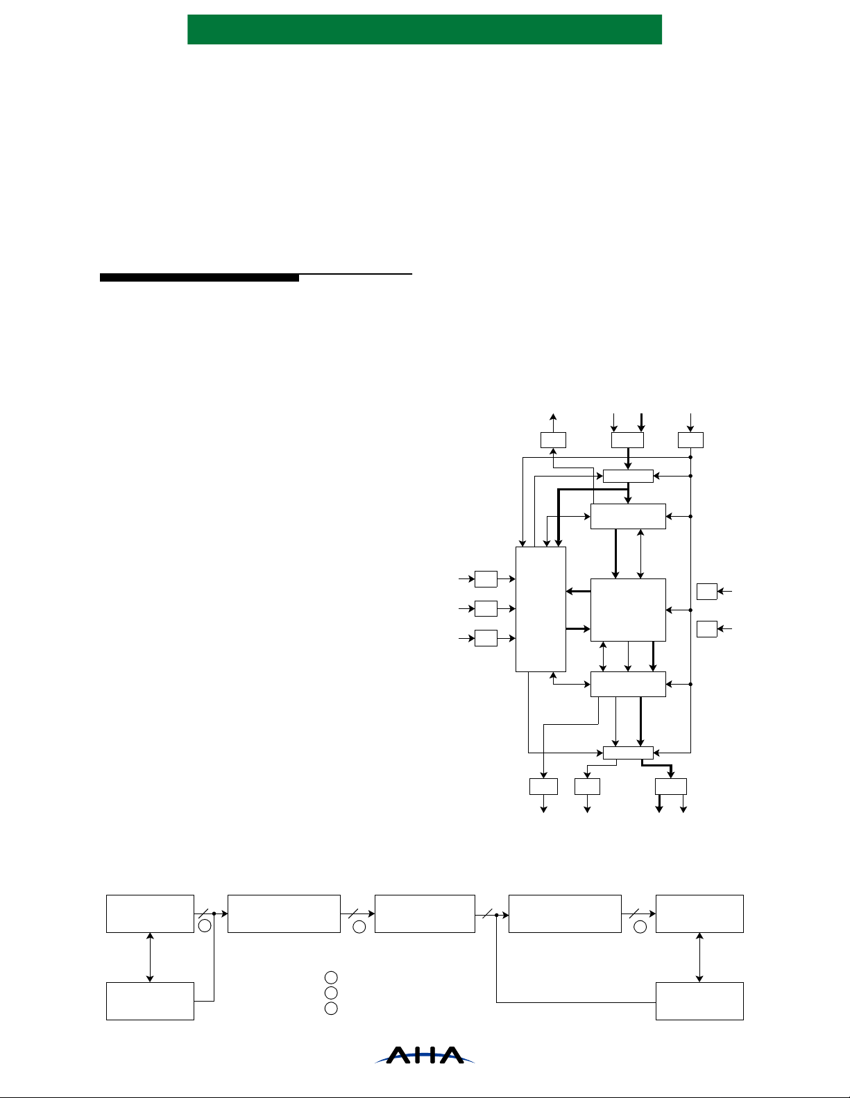
2.0 FUNCTIONAL DESCRIPTION
The ECC core has three phases of operation:
Data In, Calculation and Data Out. Data to be
This sectio n describes a n architectural
overview of the chip and its many functions,
features and operations. The block diagram for the
chip shows the Reed-Solomon ECC module, the
Input and Output Buffers, and their associated
control. All input an d output data are cl ocked on the
rising edge of CLK.
2.1 FUNCTIONAL OVERVIEW
processed is first input into a single ported Input
Buffer using a control signal DSIN. ECC core
arbitrates for the inpu t data out of the Input Buffer.
ECC core has access to the Input Buffer on clock
edges where DSIN is not asserted.
Each block is processed within the ECC core
and calculations are made. The entire block is
processed through the ECC core, and transferred
into the Output Buf fer. The device asserts RDYON
signal and holds active until the Output Buffer is
completely emptied.
The AHA4013B Reed-Solomon codec (coder/
decoder) is a member of the AHA PerFEC™ family
of high speed forward error cor rection (FEC) devices.
This single chip, three-layer metal, CMOS device can
operate in encode, decode or pas s-t hrough modes.
The ECC core implements a full error
The ECC core loads the Output Buffer in
reverse order for either operation. Data may be
strobed out of the de vice in forward or revers e order.
If forward order is desired, output data cannot be
strobed out of the device until the entire block has
been loaded into the Outpu t Buffer.
correcting Reed-Solomon decoder. This code is
capable of correct ing up t o 10 (t =10) byte- error s or
20 (t=10) erasures in a RS block.
Page 2 of 24 PS4013B-0600
Page 7
Advanced Hardware Architectures, Inc.
Gx() x αi–()
i 120=
119 R+
∏
=
The use of internal buffers is restricted per the
rules defined in Section 2.9 Data Rates and
Latencies.
Maximum delay required for each block of a
given length t o pass through the device is fixed, and
does not vary with the location or the number of
errors received. This delay (or latency), expressed
in the number of clocks i s discussed in a later
section.
2.2 CORRECTING CAPABILITY AND
POLYNOMIALS
Compared with other codes, RS codes require
relatively few “overhead” check bytes to be added
to the data stream t o ac hie ve a high degree of error
detection and correction. Since the AHA4013B
deals with bytes (or symbols) rather than with
individual bits, when a byte is in error it does not
matter how many bits within the byt e are corrupted;
it is counted as one error.
The Reed-Solomon code is defined over the
finite field GF(2
polynomial is:
and the generator polynomial, dependent on the
variable R, is given by:
8
). The field defining primitive
8
P(x) = x
+ x7 + x2 + x + 1
Correcting “erasures” takes only half as much
of the correction capa bility of the RS code as it takes
to correct “errors”, since the position information is
already known for “erasures”. The correction ab ility
of the code is bounded as:
R ≥ # erasures + 2(# errors)
Valid block length (N) is defined by the
relationship:
R + 1 ≤ N ≤ 255
where R ranges from 2 to 20.
A complete codeword can therefore ra nge from
a minimum of 3 bytes to a maximum of 255 bytes.
For further discussion on error rate
performance, refer to Section 2.10 Reed-Solomon
(ECC) Module and Error Rate Performance.
Figure 1: Block Diagram
RDYIN
RDYIN
ERASE DI[7:0] CLK
DI
REGISTER
INPUT BUFFER
367x9
CLK
where R ∈ {2, 3, 4, 5,... 20} for the AHA4013B. This
polynomial is specified in international standards ,
Intelsat IESS 308; R TCA DO-2 17 Appendix F (Rev
D) and the proposed CCITT SG-18.
For every 2 check bytes, the decoder corrects
either 2 erasures or 1 error. An erasure can be
determined with a parity detector or a signal dropout
detector external to the chip. An erasure is indicated
by the ERASE signal when the erased byte is
clocked in the device.
Figure 2: Typical Applications Diagram
ENCODER COMMUNICATIONS DECODER
DATA SOURCE
SYSTEM
CONTROLLER
8 8 8 8
A
AHA4013B
ECC COPROCESSOR
BLOCK FORMAT AT:
B C
A
KDATA PLUS R “DUMMY” BYTES
B
KDATA PLUS R CHECK BYTES
C
KDATA BYTES
CHANNEL
1 TO x BITS WIDE
RSTN
DSIN
DSON
RSTN
DSIN
DSON
CONTROL
RDYON
RDYON CRTN DO[7:0] ERR
ECC COPROCESSOR
CRTN
AHA4013B
ECC CORE
OUTPUT BUFFER
256x9
REGISTER
GND
VDD
DO
DATA SINK
SYSTEM
CONTROLLER
GND
VDD
PS4013B-0600 Page 3 of 24
Page 8

Advanced Hardwar e Architectures, Inc.
2.3 SIGNAL DESCRIPTIONS
Input Pins
DI[7:0] Data Input Bus. The input byte and ERASE
are latched on the rising edge of the clock
when both DSIN and RDYIN are activ e. If
either DSIN or RDYIN are inactive, the DI
and ERASE are ignored.
DSIN Data In put Strobe. Enables dat a from DI to
be loaded into the chip. When RDYIN is
active, DSIN being active on the rising
edge of the clock loads the input data in the
device. DSIN must be activ e f or one c lock
edge only per each input byte. DSIN is
ignored if RDYIN is inactive. Signal is
active low.
DSON Data Output Strobe. This input strobe
acknowledges to the chip that data
available on the Outpu t Bus, DO, has be en
received by the system. The device uses
this strobe to increment its internal address
counter to the next data location. DSON
must be active for one clo ck edge on ly per
each output byte. DSON is ignored if
RDYON is inactive. Active low.
ERASE Erasure input f la g fo r symbol currently on
DI. Signal is active hi gh. ERASE signal is
used for marking all check Bytes as
erasures (dummy check Bytes) during
encode operation. It is also used to mark
input symbols that contain errors during
decoding. If not used , connect this signal to
ground.
RSTN Reset. Input pin. When RSTN is active and
DSIN and DSON are inactive, the device
forces all internal control circuitry into a
known state and initializes all data path
elements. RSTN is active during
Initializat ion Phase. In this phase, intern al
registers are progr ammed by usi ng DI a nd
DSIN. Signal is active low.
CLK Clock. System clock input. Refer to
Section 4.4 AC Electrical Characteristics
for clock requirements.
Output Pins
RDYIN Ready Input. Indicate s th e chi p’s ability to
accept data input on DI. If ac ti ve, DSI N is
allowed to enable the loading of input data
on DI. When inactive, DSIN is ignored.
Signal is active low.
DO[7:0] Data Output. The output byte is available
on this bus. The val ue of the ou tpu t byte is
undefined if RDYON is inactive. Requir es
an acknowledge strobe, DSON, at a rising
edge of the clock to incre ment internal
address counter and output the next
location in the buffer. DO bus is always
driven and is not tristated by the device.
R DY O NReady Output. This output pin indicates the
chip’s ability to generate output data. If
active, DSON is allowed to increment the
internal address count er for the next data
byte. When inactive DSON i s i gnored and
DO is undefined. Signal is active low.
CRTN Correctable. The output pin when active
indicates the blo ck did not exceed th e error
threshold programmed by P. Error
threshold must be programmed with the
same value as the number of chec k symbols
R if erasures are not used. This signal is
valid when the first m essage byte, X
K−1
, of
the block is available out of the chip.
During all other times the signal is
undefined. Signal is valid for at least one
clock. Active low.
ERR Error. Output pin indicates the current
value on DO[7:0] is a corrected byte.
Active high.
2.4 PINOUT
INPUT
CLK
DI6
DI7
DISN
4443424140
GND
39
VDD
38
VDD
37
GND
36
VDD
35
RSTN
34
ERASE
33
DSON
32
RDYIN
31
RDYON
30
GND
29
GND
VDD
GND
VDD
GND
GND
VDD
*NC
*NC
VDD
GND
GND
DI0
DI1
DI2
DI3
DI4
DI5
65432
7
8
9
AHA4013B-050 PJC
10
11
12
13
14
15
16
17
1819202122232425262728
1
DO0
DO1
DO2
DO3
DO4
DO5
DO6
DO7
VDD
ERR
CRTN
OUTPUT
*NC = No connect, reserv e d for fu tur e cons i de r ati o ns .
Page 4 of 24 PS4013B-0600
Page 9
Advanced Hardware Architectures, Inc.
ECC
Core
Data Available
Reverse Order Forward Order
Data Available
.
.
.
.
.
.
X
0
Y
0
R-1
Y
K-1
X
.
.
.
.
.
.
Y
0
X
0
R-1
Y
K-1
X
Last Byte Out
First Byte Out
First
Byte
In
Last
Byte
In
. . . . . .
X
1
Y1Y
0
X
0R-2YR-1
Y
K-2XK-1
X
INPUT
BUFFER
OUTPUT
BUFFER
2.5 DATA FLOW
The device is first initialized for various
programmable parameters including: Erasure
Multiplier, Error Threshold, Number of Check
bytes, Number of Message bytes per block, Block
Length and a Control byte. Follo wing t his six-byte
initialization, the device may be used to encode,
decode or pass-through multiple blocks of data. The
device requires reinitialization when the parameters
are changed or a reset is required.
The device processes data as “blocks”
containing Message and Check Bytes. Order of
input bytes must be first mess age byte X
last messa ge byte X
Y
through last check byte Y0. The device
R−1
, followed by first check byte
0
processes the block in this manner:
- a block is clocked into the Input Buffer;
- transferred into the ECC module;
- passed to the Output Buffer in th e reverse order
from what was received at the Input Port; and
Figure 3: Data Input and Output Order
through
K−1
- clocked out through the Output Port via the
Output Buffer. Consecutive blocks may be
input into the Input Buffer while the Output
Buffer is being emptied.
Data is available through the Output Port in
forward or reverse order. Forward order clocks out
the block the same as in put and reverse order c locks
the check byte Y
through check bytes Y
0
followed by message byte X
X
.
K−1
through message byte
0
R−1
2.5.1 SHORT ENED BLOCKS
This device allows for shortened RS blocks,
thus not requiring zero padding when decoding.
During encoding, conversely, zero padding is not
performed. When the device is programmed to
decode a block of less than 255 Bytes, only the
message bytes followed by check bytes are sent.
Prepending with zero value bytes to fill out the
block to 255 Bytes is not required.
2.6 RESET AND INITIALIZATION SEQUENCE
The chip must b e r es et and initiali ze d a ny time
a reset is necessary.
Caveat: All six regist ers must be initialized
Reset and initialization first requires pulling the
RSTN low signal for at least two clocks while the
DSIN and DSON signals are held inact ive, i.e., high
Following this sequence, the six internal
registers, referred to as “Initialization Registers” are
strobed by DSIN. These bytes are loaded in order of
correctly for proper operation of the chip. The
device has no provisions for reading back
Initialization Regi ster sett ings. This seq uence must
be used if the device needs to be reset or any one
register needs updating, i.e., all registers must be
reinitialized for a change to any one register.
1 through 6.
The RSTN must be active low for at least two
clocks before the first initialization byte is strobed
in and remain active for at le ast o ne cl ock af ter the
final byte. RSTN must be high for at least two
clocks before the fi rst message byte can be strobed
into the device. For a deta iled timing diagram, see
Figure 7: Initializatio n and Reset Timing.
PS4013B-0600 Page 5 of 24
Page 10

Advanced Hardwar e Architectures, Inc.
2.6.1 INITIALIZATION REGISTERS
BYTE 1, ERASURE MULTIPLIER:
[7:0] Multiplier value tha t must be programmed
as shown in Appendix A. The table sho ws a
value to be programmed corresponding to
the block length selected.
BYTE 2, ERROR THRESHOLD:
[4:0] The threshold for determining
uncorrectability of a data block, and the
number of check bytes allocated for
correction only purposes. When not using
erasures, set to the same value as BYTE 3,
CHECK BYTES. Minimum value of 0x02
sets the Threshold t o 2 and 0x14 sets to the
maximum, 20.
[6:5] Reserved. Set to 0.
[7] Reserved. Must be set to 1.
BYTE 3, CHECK BYTES:
[4:0] Number of check bytes in RS code, R.
Minimum setting of 0x02 indicates two
check bytes for R = 2 an d 0x14 indicates the
maximum of 20.
[6:5] Reserved. Set to 0.
[7] Reserved. Must be set to 1.
BYTE 4, MESSAGE BYTES:
[7:0] Number of message bytes in code, K.
Minimum setting of 0x01 indicates 1 byte,
setting to 0xFD indicat es the maximum 253
message bytes.
BYTE 5, BLOCK LENGTH:
[7:0] Number of bytes in block, N. Setting to
0x03 indicates 3 bytes, setting to 0xFF
indicates 255 bytes.
BYTE 6, CONTROL BYTE:
[0] RESERVED Reserved. S et to 0.
[1] NOPAR Parity Symbol Control
0 Check bytes are output
following the message bytes.
1 Check bytes are not output
following the message bytes.
Correction will be done
regardless depending upo n the
bit 4, RAW, se tting.
[2] CRCTS Correction Control
0 Outputs correction vectors; to
obtain corrected data,
externally XOR the co rr ectio n
vector with the corresponding
message or check byte.
1 Outputs corrected data
[3] FOR Forward Order Control
0 Outputs the block in reverse
order
1 Outputs the block in forward
order
[4] RAW Raw Data
0 Outputs corrections or corrected
data per the CRCTS bi t
1 Outputs uncorrected, raw input
data or 0’s depending upon the
CRCTS bit setting (See table
below). NOPAR bit and
CHECK BYTE register
settings are ignored.
[5] ERC Erasure Rejection Control. This
bit is only used by the device
when the Erasures exceed the
ERROR THRESHOLD or R
settings. This bit is ignored
when the Erasures are less than
or equal to ERROR
THRESHOLD or R.
0 If Erasures are g reater tha n the
ERROR THRESHOLD or R
then erasures a re discarded and
full correction is performed.
The block is flagged
uncorrectable and the output
CRTN will be high during the
last output byte of the block.
1 If Erasures are greater than
ERROR THRESHOLD or R
then erasures a re discarded and
full correction is performed.
The output CRTN will be hig h
only when the block is
uncorrectable.
[7:6] Reserved, Set to 0.
RAW CRCTS Output
0 0 Correction vectors
0 1 Corrected data
10 Zero
1 1 Uncorrected raw input data
Page 6 of 24 PS4013B-0600
Page 11

Advanced Hardware Architectures, Inc.
2.7 ENCODE, DECODE OR PASS-THROUGH OPERATIONS
The device performs three functions: encoding,
decoding and pass-through. As an encoder the device
outputs the message block followed by “corrected”
check bytes. As a decoder, the device outputs the
corrected message bytes or correction vectors with or
without check bytes following the message. In passthrough operation, the device passes the input data as
it is received. In all three operations, the input block
flows through the Input Buffer into the ECC module
and out of the Output Buffer. Latencies for all three
operations are the same.
The device is ini tialized for t he three operati ons
as shown in the table below.
Table 1: Initialization Register Settings for Encode, Decode and Pass-Through Operations
INITIALIZATION
REGISTER
ERASURE MULTIPLIER [7:0] Appendix A value Appendix A value Appendix A value
ERROR THRESHOLD [7:0] Set to R R or less R
CHECK BYTES [7:0] Set to R R R
MESSAGE BYTES [7:0]
BLOCK LENGTH [7:0]
CONTROL BYTE
BIT(S) ENCODE DECODE P A SS-THROUGH
Set to the Number
of Message Bytes
in block, K
Set to the total of
Message and
Check bytes, N
0 (RESV) 0 0 0
1 (NOPAR) 0 System specific 0
2 (CRCTS) 1 System specific 1
3 (FOR) System specific System specific System specific
4 (RAW) 0 0 1
5 (ERC) 0 System specific 0
[7:6] Reserved 0 0 0
KK
NN
As an encoder, the device is used with the
Erasures feature enabled in the following s equence.
(Asserting the ERASE signal high enables the
Erasure feature.)
1) After init ia li zat ion, the device recei ves the
message data followed by “dummy” check
bytes. “Dummy” check bytes are clocked
into the device with the ERASE signal
asserted. The number of “dummy” check
bytes must equal R.
2) The ECC core processes the block by
“correcting” the check bytes and feeding
the codeword into the Output Buffer in
reverse order.
3) The block is then made available on the
output bus, DO. The state of the output
RDYON determines the availability of
data. ERR signal is asserted while the
“corrected check bytes” are output on the
output bus, DO. CRTN is asserted low
during the last byte out of the chip
indicating that the previous block did not
exceed the error threshold.
As a decoder, the device works similar to the
encode operation in the following sequence.
1) Following initi alization, the system clocks
the message data and the check bytes into
the Input Buffer. ERASE signal may be
asserted as desired by the system. State of
the output signal, RDYIN determines the
chip’s ability to a ccept dat a input on the DI
bus.
2) The ECC Core processes the block by
performing necessary corrections, and
feeds the codeword into the Output Buffer
in reverse order.
3) The data is available on the output port. The
state of the output signal, RDYON
determines the availa bility of valid data. An
output byte which has been corrected is
indicated by the device asserting ERR.
CRT N may be high or low d epending upon
the THRESHOLD Register and ERC bit
programmed and the errors encountered.
PS4013B-0600 Page 7 of 24
Page 12

Advanced Hardwar e Architectures, Inc.
In pass-through operation, data flows through
the device similar to the encode and decode
operations. During initialization the device is
programmed as shown above. Check Bytes are
programmed in the range of 0x02 to 0x14. The
Block length here i s the sum of Mes sage Byt es an d
Check Bytes like encode and decode modes of
operation even thou gh the device passes through the
block of data unchanged.
1) Following initialization, the system clocks
the codeword into the Inp ut Buffer.
2) The codeword is processed by the ECC
module and passed on to the Out put Buf fer
without correction.
3) The uncorrected codeword is availa ble at
the output port. State of the RDYON
determines the availabi lity of valid data.
The ERASE input is ignored during the
Input phase and ERR and CRTN outputs
are not valid.
Caveat: The device has no provisions for indicating
the start and/or en d of mess age or c heck byt es. It is
the system designer s responsi bility t o keep track of
message and check bytes transitions, if required.
processing latency period. Data is input into the
Input Buffer and processed through the ECC core.
After a processing l atency period the entire block of
data is transferred to the Output Buffer. While the
Output Buffer is bei ng emptied, the Input Buffer is
simultaneously filled with the following block at the
maximum rate. Input a nd output rates are cont rolled
by the clock speed and clocks/byte.
Continuous operation requi res a mini mum of 4
clocks/byte depending upon the block size.
Maximum data transfer rates for continuous rate
vary accordingly. Blocks may be processed
continuously through the device. If the chip is
operated with contin uous data stream s, the RDYIN
and RDYON pins will always be active (after the
initial latency). Therefore, they need not be used.
Caveat: System designe r should be awa re that data
is put into the Output Buffer in
reverse order.
Therefore, RDYON may become inactive bet ween
blocks in
forward order if data is outpu t faster than
Output Buffer is filled.
2.9 DATA RATES AND LATENCIES
2.8 BUFFERS
The Input Port contains a single-ported 367x9
buffer. The Output Port contains a single-ported
256x9 buffer. These buffers store input and output
data during the correc tion process and help maintain
the desired system data rate. A Reset ope ration as
described in the Initialization Sequen ce section
clears the buffers.
The use of internal buffers is restricted per the
rules defined in Section 2.9 Data Rates and
Latencies. These rules define the limitations of
using the buf fers to temporarily st ore more than one
block. It is highly recommended that the system
designer clearly understand these rules prior to
designing the system.
The Input Buffer rec eives input data on the DI bus
when the ECC module is i n the calculati on or in dataout phases at the desired syst em rate. The ability of the
Input Buffer to accep t dat a i s indicated by RDYIN.
The Output Buffer accepts corrected data from the
ECC during t h e d at a - o ut ph a se . RDYON is as se r ted
low when the Output Buffer is able to output data.
Data flow through t he device may occur in burst
or continuous rates. The number of clocks per byte
used to input or output determines burst or
continuous operat ing conditions. Figure 4 shows the
two operations.
Burst operation permits data to be clocked in
and out of the device at the maximum rate, i.e., 1
clock per byte. I n burst opera tion, consecu tive d ata
blocks are clocked into the device following a
This section describe s data rates and processi ng
latencies for burst and continuous operations.
Processing latenci es are the same in encode, decode
or pass-through operations. The number of clocks
used to clock in and ou t of the device determine s the
operation. The inpu t and output rates need not be the
same. No registers are required to program the
device for either operation.
Continuous block flow is achieved by us ing the
appropriate number of clocks per byte and block
length. Alternatively, data flow into and out of the
device is controlled usi ng control signals, DSIN and
DSON.
2.9.1 BURST OPERATION
Maximum processing latency , in for ward order,
expressed in number of clocks, for burst oper ation is
determined by: N × C
Definitions:
C
= input clock rate per byte. If Ci= 1, use a value
i
for C
of 2 in the latency equation
i
N = block length
R = number of check bytes
Processing Latency = Delay from first input byte to
first output byte
In reverse order, processing latency is
approximately N clocks less than above.
For a 50 MHz system using 1 clock per byte,
latencies and data rates for forward order output are
shown in the table for burst operation. Input and
Output Burs t Rates in all cases will be 50 MBytes/
+ R + 60 + N
i
Page 8 of 24 PS4013B-0600
Page 13

Advanced Hardware Architectures, Inc.
R 60
NC
m
×
C
m
1–
-----------------++
C
i
---------------------------------------- N 367≤+
sec. Note: Other frequency operations may be
derived similarly.
Output Buffer may be used to hold data from
one block while the Input Bu ffer is being fill ed with
the following block . Two rules listed in the caveats
are required to accomplish this. These ar e illustrated
Caveats:
1. Output of block i must start coinci dent with or
before the input of block i + 1.
2. Output of block i must be complete:
Processing Latency − N − 8 clocks
after the start of block i + l on the input.
in Figure 4.
Table 2: Burst Operation Using 50 MHz Clock and 1 Clock/Byte, Forward Order Output
CHECK BYTES ‘R’ = 20 CHECK BYTES ‘R’ = 2
BLOCK
LENGTHS ‘N’
MAXIMUM
LATE NCY
(# of clocks)
25 155 3.10 8.06 137 2.74 9.13
50 230 4.60 10.88 212 4.24 11.79
100 380 7.60 13.13 362 7.24 13.75
150 530 10.64 14.13 512 10.24 14.63
200 680 13.60 14.75 662 13.28 15.13
255 845 16.88 15.13 827 16.56 15.38
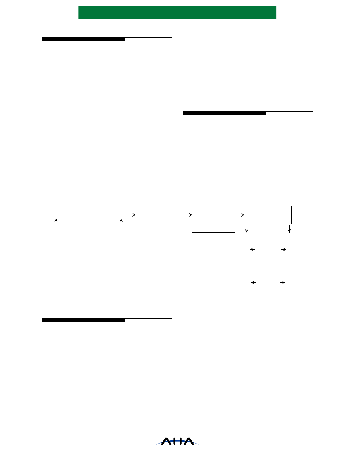
2.9.2 CONTINUOUS OPERATION
Multiple blocks of data may be processed
through the device continuou sly as shown in Figure
4. Consecutive blocks are input into the device at
the rate of C
may or may not be continuous depending on
whether parity is being output (controlled by
NOPAR) and the choice of C
operation is described by several equations. The
following terms are used in these equations:
C
- Input clock rate per byte: Ci ≥ 4 for
i
- Output clock rate per byte: Co ≥ 2
C
o
C
- Minimum of Ci and Co: If Ci < Co then
m
N - Reed-Solomon block length
K - Reed-Solomon message length
R - Reed-Solomon parity length (R = N − K)
L - Output data length: If parity is bei ng output
clocks/byte. The output data stream
i
continuous operation
C
= Ci else Cm= C
m
from the chip (NOPAR = 0), L = N; else if
the parity is not being output (NOPAR = 1)
L = K
MAXIMUM
LATENCY
(µsecs)
Average Rate
. Continuous
o
o
AVERAGE
RATE
(MBytes/sec)
--------------------------------------------------------------- -=
Maximum Latency µsec()
MAXIMUM
LATENCY
(# of clocks)
N
Equation 2:
N 1–()Ci× R 48
B. Processing Latency
Processing latency is the time from the beginning
of a block on the input to the block being ready for
output. Maximum processing latency, expressed in
number of clocks, for continuous operation is:
Equation 3:
Latency N 1–()C
C. Start and End of Output
Similar to the burst operation, Output B uffer
may be used to temporarily “hold” data from one
block while the Input Buffer is being filled.
However, these con ditions must be satisfied: the
output of a data block must start after the latency
equation (Equation 3) is satisfied, but before the
maximum delay is reached . The maximum delay is:
MAXIMUM
LATENCY
(µsecs)
NC
×
---------------
Ci1–
×=60R
i
(MBytes/sec)
NC
i
-----------------++ +≥
Cm1–
NC
-----------------+++
C
A VERAGE
RATE
×
m
×
m
1–
m
A. Conditions for Continuous Operation
The allowable input and output data rates are
related to the Reed-Solomon block length by the
following two inequali ties. C
chosen so that these equations are satisfied.
Equation 1:
PS4013B-0600 Page 9 of 24
, Co, N and K must be
i
Equation 4:
NC
×
maximum_delay 3 NC
if maximum_delay
---------------------------------------------
C
i
if maximum_delay
--------------------------------------------- 2 N, then maximum_delay× 2 NC
C
i
367, then maximum_delay 367 C
×× LC
i
o
i
---------------–×–=
C
1–
i
×=≥
××=>
i
i
Page 14

Advanced Hardwar e Architectures, Inc.
Data of one block must be fully emptied L × Co clocks after the start of empty process.
All of the conditions on the maximum delay given in Equation 4 must be satisfied. If any are not, the
output data strea m wil l begi n t o inhibit ECC processi ng. Eventually this will cause the in put buffer to over
fill and RDYIN to become inactive.
Figure 4: Burst and Continuous Operations
(Note: Blocks are shown from right to left as they are input into and output from the chip in Forward Order.
Block i is the first input block, block i + 1 is secon d in put bl ock. X
is the first input message byte of a block. Yo
K − 1
is the last input check symbol of a block. Notes 1 and 2 in burst operation are described in Section 2.9.1 Burst
Operation - Caveats.)
Burst Operation
Input Data:
Output Data:
Block i+1 Block i
. . . . . . . . . .
Y
0
X
K-1
. . . . . . . . . . . . . . . . . .
Y
0
Processing Latency
. . . . . . . . . .
Y
0 K-1
2
X
1
X
K-1
Block iBlock i+1
. . . . . . . . . .
Y
0
X
K-1
Continuous Operation
Input Data:
Output Data:
Block i+3 Block i+2 Block i+1 Block i
. . . . . . . . . . . . . . . . . . . . . . . . . . . . . . . . . . . . . . . .
Y
0
X
For a 50 MHz system using the required clocks pe r byte, max imum latenci es and da ta rates for for ward
order output are shown in the tab le f or con ti nuous operation. Input and Output rat es ar e ass umed t he same
in this table. Note: Other frequency operations are also possible.
Block i+3 Block i+2 Block i+1 Block i
. . . . . . . . . . . . . . . . . . . . . . . . . . . . . . . . . . . . . . . .
Y
0
Y
0
K-1
Y
X
K-1
0
Y
X
0
K-1
Y
X
0
K-1
Y
X
0
K-1
X
K-1
Y
X
0
K-1
X
K-1
Table 3: Continuous Operation Using 50 MHz Clock and Specified Clocks/Byte, Forward
Output Order
CHECK BYTES ‘R’ = 20 CHECK BYTES ‘R’ = 2
BLOCK
LENGTHS ‘N’
MINIMUM
REQUIRED
(clocks/byte)
25 6 8.34 5.08 5 10.0 4.26
50 5 10.00 7.75 5 10.0 7.39
100 4 12.50 12.18 4 12.5 11.82
150 4 12.50 17.52 4 12.5 17.16
200 4 12.50 22.86 4 12.5 22.50
225 4 12.50 25.52 4 12.5 25.16
255 4 12.50 28.72 4 12.5 28.36
MAXIMUM
DATA RATE
(MBytes/sec)
MAXIMUM
LATENCY
(µsecs)
MINIMUM
REQUIRED
(clocks/byte)
MAXIMUM
DATA RATE
(MBytes/sec)
MAXIMUM
LATENCY
(µsecs)
For Intelsat IESS-308, Rev F, Inner FEC Rates, use Table 4 for a system with 50 MHz clock.
Note: Other frequency operations are also possible.
Page 10 of 24 PS4013B-0600
Page 15

Advanced Hardware Architectures, Inc.
Gx() x αi–()
i 120=
119 R+
∏
=
T able 4: Continuous Operation for IESS-308 Codes Using 50 MHz Clock and Specified Clocks/Byte,
Forward Output Order
BLOCK
LENGTHS ‘N’
MESSAGE
LENGTH ‘K’
ERROR
CAPABILITY ‘t’
MINIMUM
REQUIRED
(clocks/byte)
MAXIMUM
DA TA RATE
(MBytes/sec)
MAXIMUM
LATENCY
(# of clocks)
126 112 7 4 12.5 742 14.84
194 178 8 4 12.5 1107 22.14
208 192 8 4 12.5 1181 23.62
219 201 9 4 12.5 1242 24.82
225 205 10 4 12.5 1276 25.52
Appendix B shows a spreadsheet table of block lengths vs. latencies for a 50 MHz clock system.
2.10 REED-SOLOMON (ECC) MODULE AND ERROR RATE PERFORMANCE
The module implements a full error correcting
Reed-Sol omon (RS) decoder whose function is to
perform the necessary corrections on the input
blocks. The code used by the dec ode r is capable of
generating corrections for up to 10 (t = 10) byteerrors in an RS b lock over the block length bet ween
R + 1 to 255 bytes . The number of message bytes in
an RS block, K, is equal to the RS block length
minus R (K = N − R). The RS code implemented
uses the primitive polynomial
8
P(x) = x
+ x7 + x2 + x + 1
to generate GF(256). The generator polynomial for
the code is:
An RS block consists of message and
redundancy bytes. Th e number of me ssage byte s in
the block, K, is programmable dur ing initializati on.
The number of check bytes is R and can be
programmed during in itialization to be 2 through 20
in increments of 1.
The ECC Module may be programmed to
output corrections or corrected data. If
“corrections” is selected, to obtain corrected data,
externally XOR the output correction vector with
the corresponding message or check byte. For
example, if “corrections” is selected for a block of
200 bytes with errors in locations 100, 123, 1 53, 176
and 199; output block will be 0’s for all locati ons
except for thos e positions. The bytes output at these
positions are referred to as correction vectors and
are XOR’d externally w ith the messag e bytes to
obtain the correct value. If the output of the
AHA4013B is programmed to output corrected
data, the correc ti on v ector is applied internally and
the corrected data is output.
The Symbol Error Rate Performance of the
Reed-Solomon code used is shown in Figure 5.
MAXIMUM
LATENCY
(µsecs)
Figure 5: Symbol (Byte) Error Rate Performance Curves for Codeword Length = 255 Bytes
PS4013B-0600 Page 11 of 24
-0
10
-2
10
-4
10
-6
10
-8
10
P
-10
10
-12
10
-14
10
-16
10
-0 -3
10
-1
-2
10
10
t=1 0
t=8
10-510
t=5
-4
t=3
10
t=1
-6
-7
10
-8
1010
P
Page 16

Advanced Hardwar e Architectures, Inc.
C
BER
P
UE
mN×
-------------- -=
P
UE
107–=
C
BER
10
7–
8255×
----------------- -4.910
11–
×==
The most common measures of per formance for
Reed-Solomon code are P
, PSE, and C
UE
BER
. PSE is
the probability of symbol errors and is the ratio of
the number of received symbol errors to the total
number of received symbols. In the AHA4013B
device the symbol lengt h, m, i s e qua l t o 8 b it s. P
UE
is the probability of an uncorr ectable error and is the
ratio of the number of uncor rectable cod e blocks to
the total number of received code blocks. An
uncorrectable error occurs when more than t
received symbols ar e in error . C
Bit Error Rate. The C
is the reciprocal of
BER
is the Corrected
BER
expected number of correct bits between errors.
If input noise is random, .
If with , and
P
SE
4–
810
×=t5=
.
The figure shows probability of symbol error
and uncorrectable error for block size (N) of 255. It
shows the ability of variou s levels of Reed-Solomon
error corre ction to restore the integrity of the
corrupted data. For example, using 255 byte blocks,
if 1 out of 1000 of the received bytes have one or
more bit errors, RS correction with t = 5 will restore
the data to 1 error in 2 million blocks (510 million
bytes).
For a detailed discussion on error rate
performance of Reed-Solomon c ode, ref er to AHA
Application Note, Primer: Reed-Solomon Error
Correction Codes (ECC), (ANRS01).
2.11 DETERMINING DECODER
PERFORMANCE BOUNDARIES
P = R This configuration maximizes the abili ty to
correct errors, particularly if R itself has
been chosen to be its maximum value of 20.
This is the usual choice. T his situation
causes the CRTN output t o fl ag a message
block as uncorrectable at an error level
exceeding that of which the device is
capable.
P < R This in creases the le vel of error de tection
capability. This situatio n causes the CRTN
output to flag a message block as
uncorrectable at an error level below that of
which the device is capable.
Caveat: Output block may be corrupted if a block
exceeds the correction ability of the ECC module.
2.12 ERASURES
The chip is capable of utilizing erasure
information. R erasures may be corrected in any
block assuming there are no unmarked errors.
The correction capability is: E + 2e ≤ R
Where E = number of erasures (marked errors)
e = number of unmarked errors
R= number of check symbols
If there are more than P or R erasures the
erasure information is discarded, and full error
correction is attempted. The chip can be
programmed to either call such a block
uncorrectable or not. I f pr ogr ammed not to call the
block uncorrectable (ERC bit set to 1), the ECC will
utilize the full error correction capability to decide if
the block is correctable.
AHA4013B supports a programmable feature
that allows a system designer to determine the
channel performance. This progra mmab le feature,
referred to as error threshold, P, sets a number of
errors to be allowed by the chip prior to flagging the
block uncorrectable. Erasure Rejection Control bit
of the Control Byte register determines the
condition of CRTN output pin.
P and R are both independently selectable by
the user during the Init ializat ion Contr ol Sequ ence.
The various configur ations of P and R are des cribed
as follows:
P > R This is not a sensible choice since this
implies that more check bytes are allocated
for (correction-only) purposes than there
are total check bytes (for both correction
and detection). The device will work as if P
was set equal to R.
3.0 OPERATIONAL DESCRIPTION
This section describes the relationship of
associated signals for various functions of the chip.
3.1 CLOCK
The clock input to the chip must meet the t iming
requirements shown in Fig ure 6. The chip is entirely
static thus allowing the clock to stop in either the
active or inactive state for an indefinite period
without loss of stored information.
Page 12 of 24 PS4013B-0600
Page 17

Advanced Hardware Architectures, Inc.
CLK
123
4
5
1
Figure 6: CLK Characteristics
NUMBER DESCRIPTION MINIMUM MAXIMUM UNITS
1 CLK rise time 5 nsec
2 CLK high time 8 nsec
3 CLK fall time 5 nsec
4 CLK low time 8 nsec
5 CLK period 20 nsec
All timing diagrams in this specification use the clock at the CLK pin as the reference point.
3.2 INITIALIZATION
This section describes the Rese t and Initialization Sequence timing. For a detailed discuss io n on these
sequences, refer to Section 2.6 Reset and Initialization Sequence.
Figure 7: Initialization and Reset Timing
CLK
112 2
RSTN
DSIN
DSON
3
DI
at least 2
clock cy cles
RESET
23 6145
at least 1
Input 6 bytes data for initialization
INIT IA L IZ E
clock cycle
at least 2
clock cycles
Data
NUMBER DESCRIPTION MINIMUM MAXIMUM UNITS
1 RSTN and DSIN setup time 7 nsec
2 RSTN and DSIN hold time 0 nsec
3 RSTN and DSIN assertion 2 Clock cycles
Initialization bytes are strobed into the device
while RSTN and DSIN are low d uring risi ng edges
of CLK. The R STN must be active low for at least
two clocks before the first initializat ion byte is
strobed in and remain active for at least one clock
after the final byte. Initialization register data may
be strobed at a minimum of 1 clock per byte. After
power-on the initializing registers’ contents are
undefined.
For a detailed description of the Initialization
Registers, refer to Section 2.6 Reset and
Initialization Sequence.
PS4013B-0600 Page 13 of 24
3.3 DATA INPUT
The chip latches the input data on the DI pins on
the rising edge of the CLK when DSIN and RDYIN
are both active. The two figures below show the
timing diagrams for buffer Ready and buffer Not
Ready conditions.
Page 18

Advanced Hardwar e Architectures, Inc.
1 1
1
22
22
22
22
22
111
1
11
1
valid valid
valid valid valid
valid
CLK
DI
DSIN
RDYIN
ERASE
RSTN
high = erase
1
1
22
2
2
22
2
1
1
11
1
valid
valid valid valid
valid
CLK
DI
DSIN
RDYIN
3
3
3
3
RSTN
Figure 8: Data Input - Buffer Always Ready
If RSTN is low during write, message bytes are treated as being part of the initialization sequence. If
RSTN is high, the data is treated as being part of RS block. In the example above ERASE is asserted high
in four sample clocks.
NUMBER DESCRIPTION MINIMUM MAXIMUM UNITS
1 DI, ERASE and DSIN setu p time 7 nsec
2 DI, ERASE and DSIN hold time 0 nsec
Figure 9: Data Input - Buffer Not Ready
NUMBER DESCRIPTION MINIMUM MAXIMUM UNITS
1 DI, ERASE and DSIN setu p time 7 nsec
2 DI, ERASE and DSIN hold time 0 nsec
3 RDYIN output delay 13 nsec
Any input data clocked while RDYIN is inactive are ignored. This is shown in Figure 9.
3.4 DATA OUTPUT
The DO pins are driven from a register clocked
on the rising edge of CLK.
RDYON being active. When RDYON is inactive,
data on the DO pins is undefined, and DSON is
ignored. The DSON signal acknowl edges receiving
the data and is used by the device to internally
Page 14 of 24 PS4013B-0600
Valid data on the DO pins is indicated by
increment the address counter and output the next
location in the buffer. This data output timing is
shown in Figure 10.
Page 19

Advanced Hardware Architectures, Inc.
Figure 10: Data Output
CLK
3
DO, ERR
333
valid
12 111111 122 222 22
valid va lid valid valid
DSON
444
RDYON
NUMBER DESCRIPTION MINIMUM MAXIMUM UNITS
1 DSON setup time 8 nsec
2 DSON hold time 2 nsec
3 DO output delay 3 13 nsec
4 RDYON output delay 3 13 nsec
CR TN is va li d for an RS block when the first message byte, X
, is strobed out of the c hip. Figure 1 1
K−1
shows Reverse Order output . In thi s opera tion, CRTN is valid on the last byte of the block from the Output
Buffer. In this example only message bytes are output, no check bytes.
Figure 11: CRTN Timing - Reverse Order Output
CLK
3 333
DO
Block m
Byte X
K-3
12 111111 122 222 22
DSON
CRTN
444
RDYON
Note: CRTN is active (low) if RS block m is correctable. If the number of errors detected in block m exceeds the
error threshold, P, CRTN is inactive (high).
Block m
Byte X
Block m
4
Byte X
error
VALID
See Note
correctable
K-2
Block m+1
Byte X
K-1
0
Block m+1
Byte X
1
NUMBER DESCRIPTION MINIMUM MAXIMUM UNITS
1 DSON setup time 7 nsec
2 DSON hold time 2 nsec
3 DO output delay 3 13 nsec
4 RDYON, CRTN output delay 3 13 nsec
PS4013B-0600 Page 15 of 24
Page 20

Advanced Hardwar e Architectures, Inc.
4.0 SIGNAL SPECIFICATIONS
4.1 INPUT SPECIFICATIONS
PIN
NUMBER
43 DI[7] 10 7 0 CLK
44 DI[6] 10 7 0 CLK
1DI[5] 10 7 0 CLK
2DI[4] 10 7 0 CLK
3DI[3] 10 7 0 CLK
4DI[2] 10 7 0 CLK
5DI[1] 10 7 0 CLK
6DI[0] 10 7 0 CLK
42 DSIN 10 7 0 CLK
33 DSON 10 8 2 CLK
35 RSTN 10 7 0 CLK
41 CLK 10 N/A N/A N/A
34 ERASE 10 7 0 CLK
N/A = Not Applicable
SIGNAL
NAME
(Refer to Section 4.5 DC Electrical Characteristics for pad specifications)
SELF LOAD
(maximum in pF)
4.2 OUTPUT SPECIFICATIONS
PIN
NUMBER
26 DO[7] 60 3 13 CLK
24 DO[6] 60 3 13 CLK
23 DO[5] 60 3 13 CLK
22 DO[4] 60 3 13 CLK
21 DO[3] 60 3 13 CLK
20 DO[2] 60 3 13 CLK
19 DO[1] 60 3 13 CLK
18 DO[0] 60 3 13 CLK
31 RDYON 60 3 13 CLK
32 RDY IN 60 3 13 CLK
28 CRTN 60 3 13 CLK
27 ERR 60 3 13 CLK
SIGNAL
NAME
LOAD CAP
(maximum in pF)
TSETUP
(min in nsec)
TDEL
(min in nsec)
THOLD
(min in nsec)
TDEL
(max in nsec)
STROBE
STROBE
REF
(Refer to Section 4.5 DC Electrical Characteristics for pad specifications)
4.3 POWER & GROUND PINS
PIN NUMBER SIGNAL NAME
8, 10, 11, 16, 17, 29, 30, 37, 40 GND
7, 9, 12, 15, 25, 36, 38, 39 VDD
Page 16 of 24 PS4013B-0600
Page 21

Advanced Hardware Architectures, Inc.
4.4 AC ELECTRICAL CHARACTERISTICS
CLOCK RATE
Symbol Characteristic Min Max Units Test Conditions
Fclock Clock frequency 0 50 MHz
Tlow Clock low time 8 nsec Vil to Vil
Thigh Clock high time 8 nsec Vih to Vih
Trise Clock rise time 5 nsec Vil to Vih
Tfall Clock fall time 5 nsec Vil to Vih
INPUTS
Symbol Characteristic Min Max Units Test Conditions
Tsetup Input setup time 7 nsec See Notes 1 and 3
Thold Input hold time 0 nsec See Notes 1 and 2
Notes:
1) Setup and hold times measured from a Vih on the clock input pin.
2) DSON has a 2 nsec hold time.
3) DSON has a 8 nsec setup time.
OUTPUTS
Symbol Characteristic Min Max Units Test Conditions
T out DO[7:0] Output delay 3 13 nsec See Note
Tout
Note: Output delay measured from Vih on the clock input pin to Vol/Voh on the signal pin. The output loads for
RDYON, RDYIN, ERR, CRTN
Output delay
the AC test are given in Section 4.2 Output Specifications.
3 13 nsec See Note
PS4013B-0600 Page 17 of 24
Page 22

Advanced Hardwar e Architectures, Inc.
4.5 DC ELECTRICAL CHARACTERISTICS
ABSOLUTE MAXIMUM STRESS RATINGS
Symbol Characteristic Min Max Units Test Conditions
Tstg Storage temperature -55 150 deg C
Vdd Supply voltage -0.5 6.0 V
Vin Input voltage Vss-0.5 Vdd+0.5 V
Package: 44-pin PLCC (JEDEC Standard)
OPERATING CONDITIONS
Symbol Characteristic Min Max Units Test Conditions
Vdd Supply voltage 4.75 5.25 V
Idd Supply current 1.0 mA
Idd Supply current 185 mA Dynamic
Ta Operating temperature 0 70 deg C
P Power 0.89 W
Static; Clock
stopped externally
INPUTS
Symbol Characteristic Min Max Units Test Conditions
Vih Input high voltage 2.0 Vdd V
Vil Input low voltage Vss 0.8 V 50 MHz
Iil Input leakage -10 10 µΑ 0<Vin<Vdd
Cin Capacitance 10 pF Not 100% tested
OUTPUTS
Symbol Characteristic Min Max Units Test Conditions
Voh Output high voltage 2.4 Vdd V Ioh=8mA
Vol Output low voltage Vss 0.4 V Iol=8mA
Ioh Output high current -8 mA Voh=2.4V
Iol Output low current 8 mA Vol=0.4V
Page 18 of 24 PS4013B-0600
Page 23

5.0 PACKAGING
PLCC Dimensions
A
.050
(1.27)
Packaging
B
min/max
.685/.695
(17.40/17.65)
Advanced Hardware Architectures, Inc.
Inches
(Millimeters)
C
min/max
.650/.656
(16.51/16.66)
AHA4013B-050 PJC
D
min/max
.165/.180
(4.19/4.57)
Pin 1 Identification
E
min
.020
(0.51)
C
B
F
±
.002
(0.051)
G
±
.0035
(0.089)
YYWWD-(COUNTRY OF ORIGIN)
E
F = Lead Planarity
Complete Pac kage Drawing Available Upon Request.
LLLLL
A
YYWWD = Data Code
Note:
LLLL = Lead Skew
D
G = Lead Skew
PS4013B-0600 Page 19 of 24
Page 24

Advanced Hardwar e Architectures, Inc.
6.0 ORDERING INFORMATION
6.1 AVAILABLE PARTS
PART NUMBER DESCRIPTION
AHA4013B-050 PJC 12.5 MBytes/sec Reed-Solomon Error Correction Device
6.2 PART NUMBERING
AHA 4013 B- 050 P J C
Manufacturer
Device
Number
Device Number:
4013B
Package Material Codes:
Revision
Level
Speed
Designation
Package
Material
Package Type
Test
Specification
P Plastic
Package Type Codes:
J J - Leaded Chip Carrier
Test Specifications:
C Commercial 0°C to +70°C
7.0 RELATED TECHNICAL PUBLICATIONS
PART NUMBER DESCRIPTION
PB4013B
PS4011C
PS4012B
ABRS03 AHA Application Brief – AHA4011 and AHA4012 Device Differences
ABRS04 AHA Application Brief – Reed-Solomon Evaluation Software Version 3.0
ABRS06 AHA Application Brief – AHA4011 and AHA4013 Device Differences
ABRS09 AHA Application Brief – AHA4013A and AHA4013B Device Differences
ABSTD1
ANRS01 AHA Application Note – Primer : Reed- Solomon Er ror Corr ecti on Codes ( ECC)
ANRS02 AHA Application Note – Interleaving for Burst Error Correcti on
ANRS03 AHA Application Note – Reed-Solomon Evaluation Software Version 3.0
ANRS05 AHA Application Note – Serial I/O Interface to AHA4011/AHA4012
RSEVAL Reed-Solomon Evaluation Software Version 3.0 (Windows)
IESS-308,
Appendix F
AHA Product Brief – AHA4013 12.5 MBytes/sec Reed-Solomon Error
Correction Device
AHA Product Specification – AHA4011C 10 MBytes/sec Reed-Sol omon Er ror
Correction Device
AHA Product Specificat ion – AHA4012 B 1.5 MBytes/s ec Reed-So lomon Error
Correction Device
AHA Application Brief – AHA Data Compress ion and Forward Error Correction
Standards
Concatenation of Reed-Solomon (RS) Outer Coding with the Existing Inner FEC
(Not available from AHA)
Page 20 of 24 PS4013B-0600
Page 25

APPENDIX A
Table of Elements
Advanced Hardware Architectures, Inc.
BLOCK
SIZE ‘N’
13 dd 14 3d 15 7a 16 f4
17 6f 18 de 19 3b 20 76
21 ec 22 5f 23 be 24 fb
25 71 26 e2 27 43 28 86
29 8b 30 91 31 a5 32 cd
33 1d 34 3a 35 74 36 e8
37 57 38 ae 39 db 40 31
41 62 42 c4 43 f 44 1e
45 3c 46 78 47 f0 48 67
49 ce 50 1b 51 36 52 6c
53 d8 54 37 55 6e 56 dc
57 3f 58 7e 59 fc 60 7f
61 fe 62 7b 63 f6 64 6b
65 d6 66 2b 67 56 68 ac
69 df 70 39 71 72 72 e4
73 4f 74 9e 75 bb 76 f1
77 65 78 ca 79 13 80 26
81 4c 82 98 83 b7 84 e9
85 55 86 aa 87 d3 88 21
89 42 90 84 91 8f 92 99
93 b5 94 ed 95 5d 96 ba
97 f3 98 61 99 c2 100 3
101 6 102 c 103 18 104 30
105 60 106 c0 107 7 108 e
109 1c 110 38 111 70 112 e0
113 47 114 8e 115 9b 116 b1
117 e5 118 4d 119 9a 120 b3
121 e1 122 45 123 8a 124 93
125 a1 126 c5 127 d 128 1a
129 34 130 68 131 d0 132 27
133 4e 134 9c 135 bf 136 f9
137 75 138 ea 139 53 140 a6
141 cb 142 11 143 22 144 44
145 88 146 97 147 a9 148 d5
149 2d 150 5a 151 b4 152 ef
153 59 154 b2 155 e3 156 41
157 82 158 83 159 81 160 85
161 8d 162 9d 163 bd 164 fd
165 7d 166 fa 167 73 168 e6
169 4b 170 96 171 ab 172 d1
173 25 174 4a 175 94 176 af
177 d9 178 35 179 6a 180 d4
181 2f 182 5e 183 bc 184 ff
185 79 186 f2 187 63 188 c6
HEX
VALUE
11223448
510 620 740 880
9871089119512ad
BLOCK
SIZE ‘N’
HEX
VALUE
BLOCK
SIZE ‘N’
HEX
VALUE
BLOCK
SIZE ‘N’
HEX
VALUE
PS4013B-0600 Page 21 of 24
Page 26

Advanced Hardwar e Architectures, Inc.
BLOCK
SIZE ‘N’
189 b 190 16 191 2c 192 58
193 b0 194 e7 195 49 196 92
197 a3 198 c1 199 5 200 a
201 14 202 28 203 50 204 a0
205 c7 206 9 207 12 208 24
209 48 210 90 211 a7 212 c9
213 15 214 2a 215 54 216 a8
217 d7 218 29 219 52 220 a4
221 cf 222 19 223 32 224 64
225 c8 226 17 227 2e 228 5c
229 b8 230 f7 231 69 232 d2
233 23 234 46 235 8c 236 9f
237 b9 238 f5 239 6d 240 da
241 33 242 66 243 cc 244 1f
245 3e 246 7c 247 f8 248 77
249 ee 250 5b 251 b6 252 eb
253 51 254 a2 255 c3
For example, for a block si ze of 205, the value to be pro gra med in Byte 1 of the Initialization Regi ste r
is 0xc7.
/*This is a C progr am to g enerat e Table of Elements. Pass a value of bl ock l ength, N in de cimal to th is ,
and obtain the Element value in hex.*/
int alpha(n)
int n;
{
int i,b,c;
c=01;
for (i=1;i<n;i++ ) {
b=c<<1;
if (b>0377)
c=b;
}
return c;
}
HEX
VALUE
b=b^0607;
BLOCK
SIZE ‘N’
HEX
VALUE
BLOCK
SIZE ‘N’
HEX
VALUE
BLOCK
SIZE ‘N’
HEX
VALUE
main()
{
int i;
printf("Enter N--> ");
scanf("%d",&i);
if(i<1 || i>255)
printf("1<=N<=255");
else
printf("\nN = %d\tALPHA = %2x\n\n", i, alpha(i));
}
Page 22 of 24 PS4013B-0600
Page 27

Advanced Hardware Architectures, Inc.
APPENDIX B
AHA4013B Data Rate Calculations in Continuous Operation
Assumptions and Equations:
1) 50 MHz Clock is used.
2) Input Rate (C
3) Latency =
4) Data Rate = 50 MHz/C
5) GOOD or BAD based on inequality equation:
6) GOOD or BAD based on inequality equation:
7) Check symbols are input into and output from the chip along with message symbols.
) = Output Rate (Co)
i
CiN 1–()R 60+()N
clocks/byte
i
R 60 N
------------------------------------------------- N 367≤+
N 1–()C
× R 48 N
C
i
--------------
×++×
Ci1–
C
m
----------------
×++
Cm1–
C
i
C
i
i
--------------× N
Ci1–
C
----------------×++ +≥
Cm1–
m
(5)
(6)
Note: The following tables show examples of Data Rates and Latencies for various block sizes. Other block sizes
are also possible.
CLOCKS
/BYTE
NT
MAXIMUM LATENCY
CLOCKS µSECONDS
DA TA RATE
(MB/sec)
EQUATION 5 EQUATION 6
4 25 10 209 4.18 12.50 GOOD BAD
4 50 10 343 6.86 12.50 GOOD BAD
4 53 10 359 7.18 12.50 GOOD BAD
4 75 10 476 9.52 12.50 GOOD GOOD
4 100 10 609 12.16 12.50 GOOD GOOD
4 126 7 742 14.88 12.50 GOOD G OOD
4 194 8 1107 22.16 12.50 GOOD GOOD
4 208 8 1181 23.60 12.50 GOOD GOOD
4 219 9 1242 24.88 12.50 GOOD GOOD
4 200 10 1143 22.88 12.50 GOOD GOOD
4 225 10 1276 25.52 12.50 GOOD GOOD
4 250 10 1409 28.16 12.50 GOOD GOOD
4 255 10 1436 28.72 12.50 GOOD GOOD
CLOCKS
/BYTE
NT
MAXIMUM LATENCY
CLOCKS µSECONDS
DA TA RATE
(MB/sec)
EQUATION 5 EQUATION 6
4 25 5 199 3.98 12.50 GOOD BAD
4 50 5 333 6.66 12.50 GOOD GOOD
4 75 5 466 9.36 12.50 GOOD GOOD
4 100 5 599 12.00 12.50 GOOD G OOD
4 125 5 733 14.64 12.50 GOOD G OOD
4 150 5 866 17.36 12.50 GOOD G OOD
4 175 5 999 20.00 12.50 GOOD G OOD
4 200 5 1133 22.64 12.50 GOOD GOOD
4 225 5 1266 25.36 12.50 GOOD GOOD
4 250 5 1399 28.00 12.50 GOOD GOOD
4 255 5 1426 28.56 12.50 GOOD GOOD
PS4013B-0600 Page 23 of 24
Page 28

Advanced Hardwar e Architectures, Inc.
CLOCKS
/BYTE
4 25 3 195 3.90 12.50 GOOD BAD
4 50 3 329 6.58 12.50 GOOD GOOD
4 75 3 462 9.28 12.50 GOOD GOOD
4 100 3 595 11.92 12.50 GOOD G OOD
4 125 3 729 14.56 12.50 GOOD G OOD
4 150 3 862 17.28 12.50 GOOD G OOD
4 175 3 995 19.92 12.50 GOOD G OOD
4 200 3 1129 22.56 12.50 GOOD GOOD
4 225 3 1262 25.28 12.50 GOOD GOOD
4 250 3 1395 27.92 12.50 GOOD GOOD
4 255 3 1422 28.48 12.50 GOOD GOOD
CLOCKS
/BYTE
4 25 1 191 3.82 12.50 GOOD BAD
4 50 1 325 6.50 12.50 GOOD GOOD
4 75 1 458 9.20 12.50 GOOD GOOD
4 100 1 591 11.84 12.50 GOOD G OOD
4 125 1 725 14.48 12.50 GOOD G OOD
4 150 1 858 17.20 12.50 GOOD G OOD
4 175 1 991 19.84 12.50 GOOD G OOD
4 200 1 1125 22.48 12.50 GOOD GOOD
4 225 1 1258 25.20 12.50 GOOD GOOD
4 250 1 1391 27.84 12.50 GOOD GOOD
4 255 1 1418 28.40 12.50 GOOD GOOD
NT
NT
MAXIMUM LATENCY
CLOCKS µSECONDS
MAXIMUM LATENCY
CLOCKS
µSECONDS
DA TA RATE
(MB/sec)
DA TA RATE
(MB/sec)
EQUATION 5 EQUATION 6
EQUATION 5 EQUATION 6
Page 24 of 24 PS4013B-0600
 Loading...