

Page 1

Pr oduct Specification
AHA4012B
1.5 MBytes/sec Reed-Solomon
Error Correction Device
Advanced Hardware
Architectures, Inc.
2365 NE Hopkins Court
Pullman, WA 99163-5601
509.334.1000
Fax: 509.334.9000
e-mail: sales@aha.com
http://www.aha.com
TM
Advanced Hardware
Architectures
The Data Coding Leader
PS4012B-0100
Page 2

Table of Contents
Advanced Hardware Architectures, Inc.
1.0 Introduction
1.1 Features . . . . . . . . . . . . . . . . . . . . . . . . . . . . . . . . . . . . . . . . . . . . . . . . . . . . . . . . . . . . . . . . . . . . . . . . . . . . .1
1.2 Conventions, Notations and Definitions . . . . . . . . . . . . . . . . . . . . . . . . . . . . . . . . . . . . . . . . . . . . . . . . . . . . .1
1.2.1 Definition of Correction Terms . . . . . . . . . . . . . . . . . . . . . . . . . . . . . . . . . . . . . . . . . . . . . . . . . . . . . . .2
2.0 Functional Description
2.1 Functional Overview . . . . . . . . . . . . . . . . . . . . . . . . . . . . . . . . . . . . . . . . . . . . . . . . . . . . . . . . . . . . . . . . . . .2
2.2 Correcting Capability and Polynomials. . . . . . . . . . . . . . . . . . . . . . . . . . . . . . . . . . . . . . . . . . . . . . . . . . . . . .3
2.3 Signal Descriptions. . . . . . . . . . . . . . . . . . . . . . . . . . . . . . . . . . . . . . . . . . . . . . . . . . . . . . . . . . . . . . . . . . . . .4
2.4 Pinout . . . . . . . . . . . . . . . . . . . . . . . . . . . . . . . . . . . . . . . . . . . . . . . . . . . . . . . . . . . . . . . . . . . . . . . . . . . . . . .5
2.5 Data Flow . . . . . . . . . . . . . . . . . . . . . . . . . . . . . . . . . . . . . . . . . . . . . . . . . . . . . . . . . . . . . . . . . . . . . . . . . . . .5
2.5.1 Shortened Blocks . . . . . . . . . . . . . . . . . . . . . . . . . . . . . . . . . . . . . . . . . . . . . . . . . . . . . . . . . . . . . . . . .5
2.6 Reset and Initialization Sequence. . . . . . . . . . . . . . . . . . . . . . . . . . . . . . . . . . . . . . . . . . . . . . . . . . . . . . . . . .6
2.6.1 Initialization Registers. . . . . . . . . . . . . . . . . . . . . . . . . . . . . . . . . . . . . . . . . . . . . . . . . . . . . . . . . . . . . .6
2.7 Encode, Decode or Pass-through Operations . . . . . . . . . . . . . . . . . . . . . . . . . . . . . . . . . . . . . . . . . . . . . . . .7
2.8 Buffers. . . . . . . . . . . . . . . . . . . . . . . . . . . . . . . . . . . . . . . . . . . . . . . . . . . . . . . . . . . . . . . . . . . . . . . . . . . . . . .8
2.9 Data Rate and Latencies. . . . . . . . . . . . . . . . . . . . . . . . . . . . . . . . . . . . . . . . . . . . . . . . . . . . . . . . . . . . . . . .8
2.9.1 Burst Operation . . . . . . . . . . . . . . . . . . . . . . . . . . . . . . . . . . . . . . . . . . . . . . . . . . . . . . . . . . . . . . . . . .8
2.9.2 Continuous Operation. . . . . . . . . . . . . . . . . . . . . . . . . . . . . . . . . . . . . . . . . . . . . . . . . . . . . . . . . . . . . .9
2.10 Reed-Solomon (ECC) Module and Error Rate Performance . . . . . . . . . . . . . . . . . . . . . . . . . . . . . . . . . . . .11
2.11 Determining Decoder Performance Boundaries. . . . . . . . . . . . . . . . . . . . . . . . . . . . . . . . . . . . . . . . . . . . . .12
2.12 Erasures . . . . . . . . . . . . . . . . . . . . . . . . . . . . . . . . . . . . . . . . . . . . . . . . . . . . . . . . . . . . . . . . . . . . . . . . . . . .12
3.0 Operational Description
3.1 Clock. . . . . . . . . . . . . . . . . . . . . . . . . . . . . . . . . . . . . . . . . . . . . . . . . . . . . . . . . . . . . . . . . . . . . . . . . . . . . . .12
3.2 Initialization. . . . . . . . . . . . . . . . . . . . . . . . . . . . . . . . . . . . . . . . . . . . . . . . . . . . . . . . . . . . . . . . . . . . . . . . . .13
3.3 Data Input . . . . . . . . . . . . . . . . . . . . . . . . . . . . . . . . . . . . . . . . . . . . . . . . . . . . . . . . . . . . . . . . . . . . . . . . . . .13
3.4 Data Output. . . . . . . . . . . . . . . . . . . . . . . . . . . . . . . . . . . . . . . . . . . . . . . . . . . . . . . . . . . . . . . . . . . . . . . . . .14
. . . . . . . . . . . . . . . . . . . . . . . . . . . . . . . . . . . . . . . . . . . . . . . . . . . . . . . . . . . . . . . . . . . . . . . . . . . . . .1
. . . . . . . . . . . . . . . . . . . . . . . . . . . . . . . . . . . . . . . . . . . . . . . . . . . . . . . . . . . . . . . . . . . . .2
. . . . . . . . . . . . . . . . . . . . . . . . . . . . . . . . . . . . . . . . . . . . . . . . . . . . . . . . . . . . . . . . . . .12
4.0 Signal Specifications
4.1 Input Specifications. . . . . . . . . . . . . . . . . . . . . . . . . . . . . . . . . . . . . . . . . . . . . . . . . . . . . . . . . . . . . . . . . . . .16
4.2 Output Specifications . . . . . . . . . . . . . . . . . . . . . . . . . . . . . . . . . . . . . . . . . . . . . . . . . . . . . . . . . . . . . . . . . .16
4.3 Power & Ground Pins . . . . . . . . . . . . . . . . . . . . . . . . . . . . . . . . . . . . . . . . . . . . . . . . . . . . . . . . . . . . . . . . . .17
4.4 AC Electrical Characteristics. . . . . . . . . . . . . . . . . . . . . . . . . . . . . . . . . . . . . . . . . . . . . . . . . . . . . . . . . . . . .17
4.5 DC Electrical Characteristics . . . . . . . . . . . . . . . . . . . . . . . . . . . . . . . . . . . . . . . . . . . . . . . . . . . . . . . . . . . .18
5.0 Packaging
6.0 Ordering Information
6.1 Available Parts . . . . . . . . . . . . . . . . . . . . . . . . . . . . . . . . . . . . . . . . . . . . . . . . . . . . . . . . . . . . . . . . . . . . . . .19
6.2 Part Numbering. . . . . . . . . . . . . . . . . . . . . . . . . . . . . . . . . . . . . . . . . . . . . . . . . . . . . . . . . . . . . . . . . . . . . . .20
7.0 Related Technical Publications
Appendix A
Appendix B
. . . . . . . . . . . . . . . . . . . . . . . . . . . . . . . . . . . . . . . . . . . . . . . . . . . . . . . . . . . . . . . . . . . . . . . . . . . . . . .19
. . . . . . . . . . . . . . . . . . . . . . . . . . . . . . . . . . . . . . . . . . . . . . . . . . . . . . . . . . . . . . . . . . . . . . . . . . . . . . . . .21
. . . . . . . . . . . . . . . . . . . . . . . . . . . . . . . . . . . . . . . . . . . . . . . . . . . . . . . . . . . . . . . . . . . . . . . . . . . . . . . . .23
. . . . . . . . . . . . . . . . . . . . . . . . . . . . . . . . . . . . . . . . . . . . . . . . . . . . . . . . . . . . . . . . . . . . .16
. . . . . . . . . . . . . . . . . . . . . . . . . . . . . . . . . . . . . . . . . . . . . . . . . . . . . . . . . . . . . . . . . . . . . .19
. . . . . . . . . . . . . . . . . . . . . . . . . . . . . . . . . . . . . . . . . . . . . . . . . . . . . . . . . . . . .20
PS4012B-0100
i
Page 3

Advanced Hardware Architectures, Inc.
Figures
Figure 1: Block Diagram. . . . . . . . . . . . . . . . . . . . . . . . . . . . . . . . . . . . . . . . . . . . . . . . . . . . . . . . . . . . . . . . . . . . . .3
Figure 2: Typical Applications Diagram . . . . . . . . . . . . . . . . . . . . . . . . . . . . . . . . . . . . . . . . . . . . . . . . . . . . . . . . . .4
Figure 3: Pinout . . . . . . . . . . . . . . . . . . . . . . . . . . . . . . . . . . . . . . . . . . . . . . . . . . . . . . . . . . . . . . . . . . . . . . . . . . . .5
Figure 4: Data Input and Output Order. . . . . . . . . . . . . . . . . . . . . . . . . . . . . . . . . . . . . . . . . . . . . . . . . . . . . . . . . . .5
Figure 5: Burst and Continuous Operations. . . . . . . . . . . . . . . . . . . . . . . . . . . . . . . . . . . . . . . . . . . . . . . . . . . . . .10
Figure 6: Symbol (Byte) Error Rate Performance Curves for Codeword Length = 255 Bytes. . . . . . . . . . . . . . . .11
Figure 7: CLK Characteristics . . . . . . . . . . . . . . . . . . . . . . . . . . . . . . . . . . . . . . . . . . . . . . . . . . . . . . . . . . . . . . . .12
Figure 8: Reset and Initialization Timing . . . . . . . . . . . . . . . . . . . . . . . . . . . . . . . . . . . . . . . . . . . . . . . . . . . . . . . .13
Figure 9: Data Input - Input Buffer Always Ready . . . . . . . . . . . . . . . . . . . . . . . . . . . . . . . . . . . . . . . . . . . . . . . . .13
Figure 10: Data Input - Buffer Not Ready. . . . . . . . . . . . . . . . . . . . . . . . . . . . . . . . . . . . . . . . . . . . . . . . . . . . . . . . .14
Figure 11: Data Output. . . . . . . . . . . . . . . . . . . . . . . . . . . . . . . . . . . . . . . . . . . . . . . . . . . . . . . . . . . . . . . . . . . . . . .14
Figure 12: CRTN Timing . . . . . . . . . . . . . . . . . . . . . . . . . . . . . . . . . . . . . . . . . . . . . . . . . . . . . . . . . . . . . . . . . . . . .15
ii
PS4012B-0100
Page 4

Advanced Hardware Architectures, Inc.
Tables
Table 1: Initialization Register Settings for Encode, Decode and Pass-Through Operations. . . . . . . . . . . . . . . . .7
Table 2: Burst Operation Using 6 MHz Clock and 1 Clock/Byte . . . . . . . . . . . . . . . . . . . . . . . . . . . . . . . . . . . . . . .9
Table 3: Continuous Operation Using 6 MHz Clock and Specified Clocks/Byte. . . . . . . . . . . . . . . . . . . . . . . . . .10
Table 4: Continuous Operation for IESS-308 Codes Using 6 MHz Clock and Specified Clocks/Byte . . . . . . . . .10
PS4012B-0100
iii
Page 5

Advanced Hardware Architectures, Inc.
1.0 INTRODUCTION
The AHA4012B is a single chip integrated
circuit that implements a Reed-Solomon Forward
Error Correction alg ori thm. The AHA4012B is the
lowest cost member of the AHA PerFEC family
of forward error correction (FEC) devices
conforming to the Intelsat IE S S- 308 specific ation.
Data flow through the devic e can occur in bursts at
6 MBytes per second or contin uous at 1.5 MBytes
per second maximum.
The device supports several programmable
parameters, including; block size, error threshold,
number of check bytes and mode of operations.
Shortened blocks are supported without requirement of zero padding. The dat a input port is u sed to
initialize the progr ammable parameters a nd the two
on-chip buffers are used to input and output data.
Discontinuities in data flow may be controlled by
dedicated control pins.
High operating frequenc y, in put and output data
rate flexibility, low processing latency and various
programmable parameters make this device ideal
for many applications including: DTV, DBS,
ADSL, Satellite Communications, ISDN, High
Performance Modems and networks.
This specification provides full electrical and
mechanical information to help a system engineer
develop a system using AHA401 2B. This document
contains descriptions on correction terms, pinout,
functions and featu res , DC and AC ch ar acteristics,
package and mechanical specifications, ordering
information and Related Technical Publications.
Software simulat ion of the RS code as implemented
in the device is also available. Please contact AHA
or its authorized sa les representatives worldwide for
copies of Related Technical Publications and
software simula t io n.
1.1 FEATURES
PERFORMANCE:
• Polynomial complies to Int elsat IESS-308;
RTCA DO-217 Appendix F, Revision D and
proposed ITU-TS SG-18 (Formerly CCITT SG-
18) Standards
• 6 MBytes/sec burst transfer rate with a 6 MHz
clock for all block lengths
• Maximum channel rate of 1.5 MBytes/sec
continuous for block lengths from 54 bytes
through 255 bytes using a 6 MHz clock
• Processi n g latency tim e less than 101 µsec in
continuous operation for block lengths of 100
bytes
FLEXIBILITY:
• Programmable to correc t fro m 1 to 10 error by tes
or 20 erasure bytes per block
• Block lengths programmable from 3 to 255 bytes
• Encode, decode or pass-through capabi li ty inline with data flow
• Continuous or burst mode operation
• Programm a ble error th re shold to help determine
channel performance
SYSTEM INTERFAC E:
• Byte wide synchronous I/O ports with internal
buffering on both ports
• Input data pins used for programmable
parameters
• Dedicated control pins permit discontinuities in
system data flow
OTHERS:
• 44 pin PLCC; 50 mil lead pitch
• Pin and plug compatible with the higher
performance AHA4011
• Software emulation of the algorithm available
1.2 CONVE NTIONS, NOTATIONS AND
DEFINITIONS
– Certain signals are logically true at a voltage
defined as “low” in the dat a sheet. All such signals
have an “N” appended to the end of the signal
name. For example, RSTN and DSON.
– “Signal assertion” means the output signal is
logically true.
– Hex values are defined with a pr efix of “0x” , such
as “0x10”.
– A range of signal names is denoted by a set of
colons between t he number s. Most sign ific ant bi t
is always shown first, followed by least significan t
bit. For example, DI[7:0] represents Data Input
Bus 7 through 0.
– A product of two variables is expressed with an
“×”, for example, N × C
Length multiplied by Input clocks/byte.
– Mega Bytes per second is referred to as MBytes/
sec or MB/sec.
– Channel Rate is defined as transfer rate includi ng
user data and error correction check bytes.
represents Codeword
i
PS4012B-0100 Page 1 of 24
Page 6

Advanced Hardware Architectures, Inc.
1.2.1 DEFINITION OF CORRECTION T E RMS
TERM
NAME
(other references)
Message Length
K
(user data or message
bytes)
Check symbols
R
(parity or redundan cy)
Codeword Length
N
(block lengt h)
t Error Corrections
P Error Threshold
e Number of Errors
E Number of Erasures
G Burden of Correction
DEFINITION
Number of user data symbols in one message bloc k.
Size of a symbol in AHA4012B is 8-bits. Message
length is K = N − R. The first message byte is
referred to as X
Symbols appended to the user data to detect and
correct errors. The number of check symbols
required in a system is R ≤ E + 2e.* The first check
symbol is referred to as Y
.
is Y
0
Sum of message and check symbols. N = K + R.
Maximum number of error corrections performed
by the device. The value is t = Integer .
The threshold limit to determine uncorrectability
of a Codeword and the number of check bytes
allocated for correct io n-only pur po ses (not for
detection).
An error is defined as an erroneous byte whose
correct value and position within the message
block are both unknown.
An erasure is defined as a n error whose posi tion is
known within the message block.**
A measure of the bur den of correction bein g placed
on the capabilities of the device for that message
block. The value G = 2e + E.
; the last message byte is X0.
K−1
; the last check symbol
R−1
NK–
-------------2
RANGE
(number of bytes)
1 through 253
(1, 2, 3, 4 . . . 253)
2 through 20 in
increments of 1
(2, 3, 4 . . . 20)
3 through 255
(3, 4, 5, 6 . . . 255)
1 through 10
(1, 2, 3 . . . 10)
2 through 20
(2, 3, 4 . . . 20)
0 through N
0 through N
0 through R
* For every 2 check bytes, the AHA4012B can correct either 2 erasures or 1 error.
** An erasure is detected by a parity detector or a signal dropout detector. The presence of an erasure is
indicated by asserting the ERASE signal when the erased byte is clocked into the AHA4012B.
2.0 FUNCTIONAL DESCRIPTION
This section describes an architectural
overview of the chip and its many functions,
features and operating modes. The block diagram
for the chip sh ows the Reed-Solomon ECC mod ule,
the Input and Output Buffers and their associated
control. All input an d output data are cl ocked on the
rising edge of CLK.
2.1 FUNCTIONAL OVERVIEW
The AHA4012B Reed-Solomon codec (coder/
decoder) is the lowest cost member of the AHA
PerFEC
devices. This single chip, three-layer metal, CMOS
device can operate in encode, decode or passthrough modes.
TM
family of forward error correction (FEC)
The ECC core imp lements a full err or
correcting R eed-Solomon decoder. This code is
capable of correct ing up to 10 (t = 10 ) byte-errors or
20 (t = 10) erasures in a block.
Page 2 of 24 PS4012B-0100
Page 7
Advanced Hardware Architectures, Inc.
R
# erasures 2 # errors()+≥
The ECC core has three phases of operation:
Data In, Calculation and Data Out. Data to be
processed is first input into a singl e po rted Input
Buffer using a control signal DSIN. ECC core
arbitrates fo r the input data out of th e Input Buffer.
ECC core has access to the Input Buffer on clock
edges where DSIN is not asserted.
Each block is processed within the ECC core
and calculations are made. The entire block is
processed through the ECC core and transferred
into the Output Buf fer. The device asserts RDYON
signal and holds active until the Output Buffer is
completely emptied.
The ECC core loads the Output Buffer in
reverse order fo r either mode. Da ta is strobed o ut of
the device in forward order.
The use of internal buffers is restricted per the
rules defined in Section 2.9
Latencies
.
Data Rate and
Maximum delay required for each block of a
given length to pass thr ough the de vice is fixed and
does not vary with the location or the number of
errors received. This delay (or latency), expressed
in the number of clocks is discussed in a later
section.
2.2 CORRECTING CAPABILITY AND
P OLYNOMIALS
For every 2 check bytes, the de c oder corrects
either 2 erasures or 1 error. An erasure can be
determined with a parity detector or a signal dropout
detector external to the chip. An erasure is indicated
by the ERASE signal when the erased byte is
clocked into the device.
Correcting “erasures” takes only half as much
of the correction capa bility of the RS code as it takes
to correct “err ors”, since the p osition informat ion is
already known for “er asures”. The correction abil ity
of the code is bounded as:
Valid block length (N) is defined by the
relationship:
1
R
255≤≤+
N
where R ranges from 2 to 20.
A complete codeword can therefore ra nge from
a minimum of 3 to a maximum of 255 bytes.
For further discussion on error rate
performance, refer to Section 2.10
(ECC) Module and Error Rate Performa nce
Reed-Solomon
.
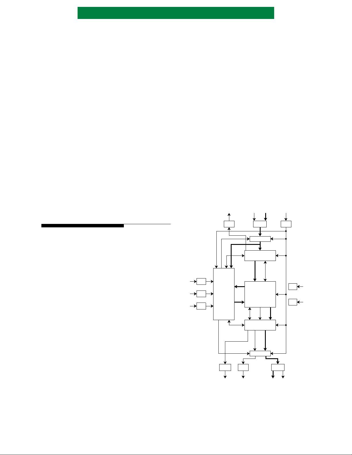
Figure 1: Block Diagram
RDYIN
RDYIN CLK
ERASE DI[7:0] CLK
DI
Compared w ith other codes , RS codes require
relatively few “overhead” check bytes to be added
to the data stream to achieve a high degree of er ror
detection and correction. Since the AHA4012B
deals with bytes (or symbols) rather than with
individual bits, when a byte is in error it does not
matter how many bits within the byt e are corrupted;
it is counted as one error.
The Reed-Solomon code is defined over the
finite field GF(28). The field defining primitive
polynomial is:
Px()x8x7x2x
1++++=
and the generator polynomial , dep endent on the
variable R, is given by:
119R+
()
Gx
=
∏
i
αi–()
x
120=
where R {2, 3, 4, 5, . . . 20} for the AHA4012B.
This polynomial is specifie d in international
standards, Intelsat IESS-308; RTCA DO-217
Appendix F, Revision D and the proposed ITU-TS
SG-18 (Formerly CCITT SG-18).
REGISTER
INPUT BUFFER
367x9
RSTN
RSTN
DSIN
DSON
DSIN
DSON
CONTROL
RDYON
RDYON CRTN DO[7:0] ERR
ECC CORE
OUTPUT BUFFER
REGISTER
CRTN
256x9
DO
A typical system bloc k diagram is shown in the
following figure.
GND
VDD
GND
VDD
PS4012B-0100 Page 3 of 24
Page 8
Advanced Hardware Architectures, Inc.
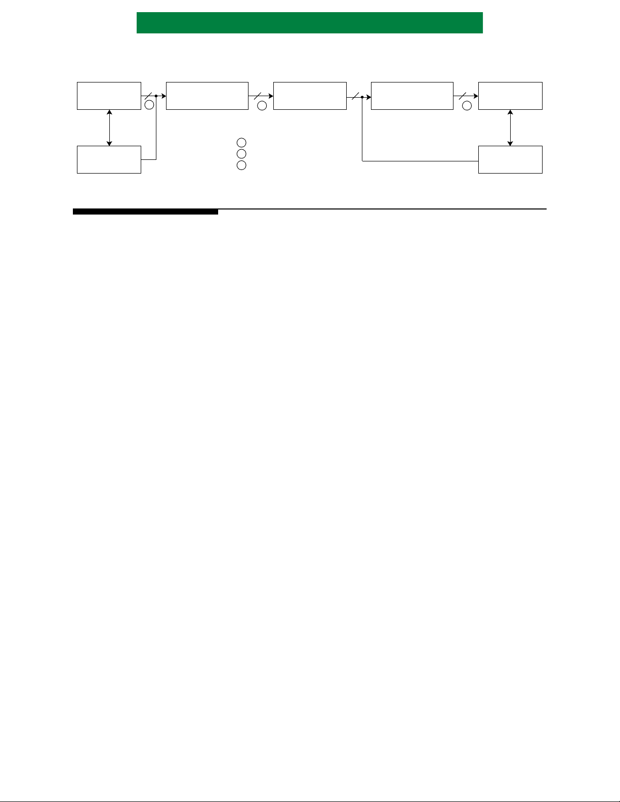
Figure 2: Typical Applications Diagram
ENCODER COMMUNICATIONS DECODER
DATA SOURCE
SYSTEM
CONTROLLER
8 8 8 8
A
AHA4012B
ECC COPROCESSOR
BLOCK FORMAT AT:
A
B
C
B C
KDATA PLUS R “DUMMY” BYTES
KDATA PLUS R CHECK BYTES
KDATA BYTE S
2.3 SIGNAL DESCRIPTIONS
CHANNEL
1 TO x BITS WIDE
AHA4012B
ECC COPROCESSOR
DATA SINK
SYSTEM
CONTROLLER
Input Pins
DI[7:0] Data Input Bus. The input byte and ERASE
are latched on the rising edge of the clock
when both DSIN and RDYIN are active. I f
either DSIN or RDYIN are inactive, the DI
and ERASE are ignored.
DSIN Data Input Strobe. Enables data from DI to
be loaded into the chip. When RDYIN is
active, DSIN being active on the rising
edge of the cl ock loads the input data i n the
device. DSIN must be activ e for o ne c lock
edge only per each input byte. DSIN is
ignored if RDYIN is inactive. Signal is
active low.
DSON Data Output Strobe. This input strobe
acknowledges to the chip that data
available on the Outpu t Bus, DO, has be en
received by the system. The device uses
this strobe to increment its internal address
counter to the next data location. DSON
must be active for one clock edge only p er
each output byte. DSON is ignored if
RDYON is inactive. Active low.
ERASE Erasure input flag fo r symbol currently on
DI. Signal is active high. ERASE signal is
used for marking all check Bytes as
erasures (dummy check Bytes) during
encode operation. It is also used to mark
input symbols that contain errors during
decoding. If not used, conn ect this signal to
ground.
RSTN Reset. Input pi n. When RSTN is active and
DSIN and DSON are inactive, the device
forces all internal control circuitry into a
known state and initializes all data path
elements. RSTN is active during
Initialization Phase. In this phase, chip
parameters are programmed by using DI
and DSIN. Signal is active low.
CLK Clock. System clock input. Refer to
Section 4.4
for clock requirements.
AC Electrical Characteristics
Output Pins
RDYIN Ready Input. Indicates the chip's abili t y to
accept data input on DI. If ac tive, DSIN is
allowed to enable the loading of input data
on DI. When inactive, DSIN is ignored.
Signal is active low.
DO[7:0] Data Output. The output byte is available
on this bus. The val ue of the outpu t byte is
undefined if RDYON is inactive. Requ ires
an acknowledge strobe, DSON, at a rising
edge of the clock to increment internal
address counter and output the next
location in the buffer. DO bus is al w ays
driven and is not tristated by the device.
R D Y O NReady Output. This output pin indicates the
chip's abil ity to gener ate output data. If
active, DSON is allowed to increment the
internal address counter for the next data
byte. When inactive DSON is ignored and
DO is undefined. Signal is active low.
CRTN Correctable. The output pin when active
indicates the blo ck did not exceed th e error
threshold programmed by P. Error
threshold must be programmed with the
same value as the number of chec k symbols
R if erasures are not used. This signal is
valid when the first mess age byte , X
the block is available out of the chip.
During all other times the signal is
undefined. Signal is valid for at least one
clock. Active low.
ERR Error. Output pin indicates the current
value on DO[7:0] is a corrected byte.
Active high.
K−1
, of
Page 4 of 24 PS4012B-0100
Page 9
Advanced Hardware Architectures, Inc.
2.4 PINOUT
Figure 3: Pinout
INPUT
DI0
DI1
DI2
DI3
65432
7
VDD
8
GND
9
VDD
10
GND
11
GND
12
VDD
13
*NC
*NC
VDD
GND
GND
AHA4012B-006 PJC
14
15
16
17
1819202122232425262728
DO0
DO1
DO2
DO3
OUTPUT
*NC = No connect, reserved for future considerations.
2.5 DATA FLOW
DI4
DI5
DI6
1
4443424140
DO4
DO5
DO6
DI7
DISN
TM
DO7
VDD
CLK
ERR
GND
CRTN
39
38
37
36
35
34
33
32
31
30
29
VDD
VDD
GND
VDD
RSTN
ERASE
DSON
RDYIN
RDYON
GND
GND
device requires reinitialization only when the
parameters are changed or a reset is required.
The device processes data as “blocks”
containing Message and Check Bytes. Order of
input bytes must be f irst message byte X
last message byte X
through last check byte Y0. The device
Y
R−1
, followed by first check byte
0
through
K−1
contains an internal counter to keep track of start
and end of block. No external signal is required to
indicate start and end of block. The device processes
the block in this manner:
- a block is clocked into the Input Buffer;
- transferred into the ECC module ;
- passed to t he Output Buffer in the reverse order
from what was received at the Input Port; and
- clocked out through the Output Port via the
Output Buffer. Consecutive blocks may be
input into the Input Buffer while the Output
Buffer is be ing emptied.
Data is available through the Output Port in
forward order . Data is clocked out in the same order
as it is input.
2.5.1 SHORTENED BLOCKS
The device is first initialized for various
programmable parameters including: Erasure
Multiplier, Error Threshold, Number of Check
bytes, Number of Message bytes per block, Block
Length and a Control byte. Following t his six-byte
initialization, the device may be used to encode,
decode or pass-through multiple blocks of data. The
Figure 4: Data Input and Output Order
. . . . . .
Y1Y
0
Last
Byte
In
X
Y
X
1
0R-2YR-1
X
K-2XK-1
First
Byte
In
INPUT
BUFFER
This device allows for shortened RS blocks,
thus not requiring zero padding when decoding.
During encoding, converseley, zero padding is not
performed. When the device is programmed to
decode a block of less than 244 Bytes, only the
message Bytes followed by check Bytes are sent.
Prepending with zero value Bytes to fill out the
block to 255 Bytes is not required.
ECC
Core
OUTPUT
BUFFER
Data Available
Forward Order
Last Byte Out
First Byte Out
Y
0
.
.
.
Y
R-1
X
0
.
.
.
X
K-1
PS4012B-0100 Page 5 of 24
Page 10

Advanced Hardware Architectures, Inc.
2.6 RESET AND INITIALIZATION SEQUENCE
Reset and initialization first requires pulling the
RSTN low signal for at least two clocks wh ile the
DSIN and DSON signals are held inactive, i.e.,
high.
Following this sequence, the six internal
registers, refer red to as “Initializ ation Registers” are
strobed by DSIN. These byte s are loaded in orde r of
1 through 6.
The RSTN must be active low for at least two
clocks before the fi rst initialization byte is strobed
in and remain active for at least one clock after the
final byte. RSTN must be high for at least two
clocks before the first message byte can be strobed
into the device. For a detailed timing diagram, see
Figure 8
a reset is necessary.
correctly for proper operation of the chip. The
device has no provisions for reading back
Initialization Regist er setti ngs. This sequenc e must
be used if the device needs to be reset or any one
register needs updating, i.e., all registers must be
reinitialized for a change to any one register.
2.6.1 INITIALIZATION REGISTERS
BYTE 1, ERASURE MULTIPLIER:
[7:0] Multiplier value that must be programmed
BYTE 2, ERROR THRESHOLD:
[4:0] The threshold for determining
[6:5] Reserved. Set to 0.
[7] Not used. Don't care.
BYTE 3, CHECK BYTES:
[4:0] Number of check bytes in RS code, R.
[6:5] Reserved. Set to 0.
[7] Not used. Don't care.
: Reset and Initialization Timing
The chip must b e reset and initialize d any time
Caveat: All six registers must be initialized
as shown in Appendix A. The table sho ws a
value to be programmed corresponding to
the block length selected.
uncorrectability of a data block, and the
number of check bytes allocated for
correction-only purposes. When not using
erasures set to the sa me value as BYTE 3,
CHECK BYTES. Minimum value of 0x02
sets the Threshold t o 2 and 0x14 sets to the
maximum, 20.
Minimum setting of 0x02 indicates two
check bytes for R = 2 an d 0x14 indicates the
maximum of 20.
.
BYTE 4, MESSAGE BYTES:
[7:0] Number of message bytes in code, K.
Minimum setting of 0x01 ind ica tes 1 byte,
setting to 0xFD indicat es the maximum 253
message bytes.
BYTE 5, BLOCK LENGTH:
[7:0] Number of bytes in block, N. Setting to
0x03 indicates 3 bytes, setting to 0xFF
indicates 255 bytes.
BYTE 6, CONTROL BYTE:
[0] RES Reserved. Set to 0.
[1] NOPAR Parity Symbol Control
When set to 0, check byt es ar e
output following the message
bytes.
When set to 1, check byt es ar e
not output following the
message bytes. Co rrection will
be done regardless depending
upon the bit 4, RAW, setting.
[3:2] RES Reserved. Set both bits t o1.
[4] RAW Raw Data
When set to 0, outputs
corrected data.
When set to 1, outputs raw
uncorrected input data.
[5] ERC Erasure Rejection Control.
This bit is only used by the
device when the Erasures
exceed the ERROR
THRESHOLD or R settings.
This bit is ignored when the
Erasures are less than or equal
to ERROR THRESHOLD
or R.
When set to 0, if Erasures are
greater than the ERROR
THRESHOLD or R then
erasures are discar ded and full
correction is performed. The
block is flagged uncorrectable
and the output CRTN will be
high during the first message
byte of the block.
When set to 1, if Erasures are
greater than ERROR
THRESHOLD or R then
erasures are discar ded and full
correction is performed. The
output CR TN will be high only
when the block is
uncorrectable.
[7:6] Reserved, Set to 0.
Page 6 of 24 PS4012B-0100
Page 11

Advanced Hardware Architectures, Inc.
2.7 ENCODE, DECODE OR PASS-THROUGH OPERATIONS
The device performs three functions: encoding, decoding and pass-through. As an encoder the device
outputs the message block followed by “corrected” check bytes. As a decoder, the device outputs the
corrected message b ytes with o r without c heck bytes fol lowing the message. In pass-t hrough operat ion, the
device passes the i nput data a s it is re ceived . In all th ree opera tions, the input bloc k flows t hrough the I nput
Buffer into the ECC module and out of the Output Buffer. Latencies for all three operations are the same.
The device is in itialized for the three opera tions as shown in the table be low.
Table 1: Initialization Register Settings for Encode, Decode and Pass-Through Operations
INITIALIZATION REGISTER BIT(S) ENCODE DECODE PASS-THROUGH
ERASURE MULTIPLIER [7:0] Appendix A Value Appendix A Value Appendix A Value
ERROR THRESHOLD [7:0] Set to R R or less R
CHECK BYTES [7:0] Set to R R R
Set to the Number
MESSAGE BYTES [7:0]
BLOCK LENGTH [7:0]
[7:6] Reserved 0 0 0
5(ERC)000
CONTROL BYTE
4(RAW)001
[3:2] Reserved 1 1 1
1(NOPAR) 0 System specific 0
0(RESV)000
of Message Bytes
in block, K
Set to the tota l of
Message and
Check bytes, N
KK
NN
As an encoder, the device is used with the
Erasures featur e enabled in t he following s equence.
(Asserting the ERASE signal high enables the
Erasure feature . )
1) After initiali zation, the device receives t he
message data followed by “d ummy” check
bytes. “Dummy” check bytes are clocked
into the device with the ERASE signal
asserted. The number of “dummy” check
bytes must equal R.
2) The ECC core processes the block by
“correcting” the check bytes and feeding
the codeword into the Output Buffer in
reverse order.
3) The block is then made available on the
output bus, DO. The state of the output
RDYON determines the availability of
data. ERR signal is asserted while the
“corrected check bytes” are output on the
output bus, DO. CRTN is asserted low
during the first mes sage byte out of the chip
indicating that the bloc k did not exceed the
error thres ho ld.
As a decoder, the device works similar to the
encode operation in the following sequence.
1) Following initialization, the system clocks
the message data and the check bytes into
the Input Buffer. ERASE signal may be
asserted as desired by the system. State of
the output signal, RDYIN determines the
chip’ s abi lity to a ccept dat a input on the DI
bus.
2) The ECC Core processes the block by
performing necessa ry corrections and feeds
the codeword into the Output Buffer in
reverse order.
3) The data is available on the output port. The
state of the output signal, RDYON
determines the availa bility of valid data. An
output byt e wh ich has bee n corrected is
indicated by the device asserting ERR.
CRT N may be high or low depending up on
the THRESHOLD Register and ERC bit
programmed and the errors encountered.
PS4012B-0100 Page 7 of 24
Page 12

Advanced Hardware Architectures, Inc.
NC
i
×
R60N
++ +
In pass-through operation, data flows through
the device similar to the Encode and Decode
operations. During initialization the device is
programmed as shown above. Check Bytes are
programmed in the range of 0x02 to 0x14.5. The
Block length here is the sum of message Bytes and
Check Bytes like encode and decode modes of
operation even thou gh the device passes through t he
blocks of data unchanged.
1) Following initialization, the system clocks
the codeword into the In put Buffer.
2) The codeword is processed by the ECC
module and passed on to the Out put Buf fer
without correction.
3) The uncorrected codeword is available at
the output port. State of the RDYON
determines the availability of valid data.
The ERASE input is ignored during the
Input phase and ERR and CRTN outputs
are not valid.
Caveat: The device has no provis ions for indicating
the start and/or en d of mess age or c heck byt es. It is
the system designer s responsi bility t o keep track of
message and check bytes transitions, if required.
2.8 BUFFERS
The Input Port contains a single-ported 367x9
buffer. The Output Port contains a single-ported
256x9 buffer. These buffers store input and output
data during the correc tion process and help maintain
the desired system data rate. The buffers suppor t the
ECC module during its operation phases: Data in,
Calculation and Data out. A Reset operation as
described in Section 2.6
Sequence
clears the buffers.
The use of internal buffers is restricted per the
rules defined in Section 2.9
Latencies
. These rules define the limitations of
using the buf fers to temporarily stor e more than one
block. It is highly recommended that the system
designer clearly understand these rules prior to
designing the system.
The Input Buffer receives input data on the DI
bus when the ECC module is in the calculat ion or in
data-in phases at the desired system rat e. The ability
of the Input Buff er to accept data is indic ated by
RDYIN.
The Output Buffer accept s corre cted data fr om
the ECC during the data-out phase. Corrections are
placed in the buffer at 1 clock per byte by the ECC
module to be removed by the system at its desired
rate. RDYON is asserted low when the Output
Buffer is able to out put data.
Reset and Initialization
Data Rate and
2.9 DATA RATE AND LATENCIES
This section descri bes data rates and proces sing
latencies for burst and continuous operations.
Processing latenci es are the same in encode, decode
or pass-through mode operations.
The input and output rates need not be the same
for burst and conti nuous operations. No registers ar e
required to program th e device for either operation.
Continuous block fl ow is achieved by us ing the
appropriate number of clocks per byte and block
length. Alternatively, data flow into and out of the
device is controlled usi ng control signals, DSIN and
DSON.
2.9.1 BURST OPERATION
Maximum processing latency , i n forward order,
expressed in numb er of clocks, for burst operation is
determined by:
Definitions:
= input clock rate per byte. If Ci=1, use a value
C
i
N = block length
R = number of check bytes
Processing Latency = Del ay from first input byte t o
For a 6 MHz system using 1 clock per byte,
latencies and da ta rates are shown in the table for
burst operation. Inp ut and Output Burst Rat es in all
cases will be 6 MByt es/sec. Note: Other frequency
operations may be derived similarly.
Output Buffer may be used to hold data from
one block while the Input Buf fer is being filled wi th
the following block. Two rules listed in the caveats
are required to accomplish this. These are illustrated
in Figure 5
Caveats:
1. Output of block i must start c oincident with or
2. Output of block i must be complete:
of 2 in the latency equation.
for C
i
first output byte
: Burst and Continuous Operations
.
before the input of block i + 1.
Processing Latency − N − 8 clocks after the
start of block i + l on the input.
Page 8 of 24 PS4012B-0100
Page 13

Advanced Hardware Architectures, Inc.
Table 2: Burst Operation Using 6 MHz Clock and 1 Clock/Byte
CHECK BYTES ‘R’ = 20 CHECK BYTES ‘R’ = 2
BLOCK
LENGTHS ‘N’
MAXIMUM
LATENCY
(# of clocks)
MAXIMUM
LATENCY
(µsecs)
AVERAGE
RATE
(MBytes/sec)
MAXIMUM
LATENCY
(# of clocks)
MAXIMUM
LATENCY
(µsecs)
25 155 26 1.0 137 23 1.1
50 230 38 1.3 212 35 1.4
100 380 63 1.6 362 60 1.7
150 530 89 1.7 512 85 1.8
200 680 113 1.8 662 111 1.8
255 845 141 1.8 827 138 1.8
Average Rate
2.9.2 CONTINUOUS OPERATION
---------------------------------------------------------------=
Maximum Latency (µsec)
N
B. Processing Latency
Processing latency is the time from the
Multiple blocks of data may be processed
through the device conti nuously as shown in Figure
: Burst and Continuous Operations
5
blocks are input into the device at the rate of C
. Consecutive
i
beginning of a blo ck on the i nput to the block being
ready for output. Maximum processing latency,
expressed in number of clocks, for continuous
operation is:
clocks/byte. Data may be out put in bursts depending
on whether parity is being output (controlled by
NOPAR) and the choice of C
. Continuous
o
operation is described by several equations. The
Equation 3:
Latency
1–()
C
×=60
N
i
following terms are used in these equations:
- Input clock rate per byte: Ci ≥ 4 for
C
i
continuous operation
- Output clock rate per byte: Co ≥ 2
C
o
- Minimum of Ci and Co: if Ci < Co then
C
m
= Ci; else Cm = C
C
m
o
N - Reed-Solomon block length
K - Reed-Solomon message length
R - Reed-Solomon parity length (R = N − K)
L - Output data length – If parity is being
output from the chip (NOPAR = 0), L = N;
if the parity is n ot being output
(NOPAR = 1), L = K
A. Conditions for Continuous Operation
The allowable input and output d a ta rates are
related to the Reed-Solomon block length by the
following two inequaliti es. C
chosen so that these equations are satisfied.
, Co, N and K must be
i
C. Start and End of Output
Similar to the burst operation, Output Buffer
may be used to temporarily “hold” data from one
block while the Input Buffer is being fill ed .
However, these conditions must be satisfied: the
output of a data block must start after the latency
equation (Equation 3) is satisfied, but before the
maximum delay is reached . The maximu m delay is :
Equation 4:
maximum_delay 3
if maximum_delay
---------------------------------------------
C
i
if maximum_delay
---------------------------------------------
C
i
367, then maximum_delay 367
2N, then maximum_delay× 2
Data of one block must be fully empt ied L × Co
××
NC
i
clocks after the start of empty process.
Equation 1:
Equation 2:
N
NC
60
×
C
i
-----------------++
C
C
i
R
R
----------------------------------------
1–()
×
m
48
m
1–
N
NC
---------------
C
i
×
367≤+
i
1–
×
NC
m
-----------------++ +≥
1–
C
m
All of the conditions on the maximum delay
given in Equation 4 must be satisfied. If any are not,
the output data stream will begin to inhibit ECC
processing. Eventually this will cause the input
buffer to over fill and R DYIN to bec o me inactive .
AVERAG E
RATE
(MBytes/sec)
×
NC
m
-----------------+++
R
LC
C
m
o
1–
×
NC
---------------–×–=
1–
C
i
i
×=≥
C
××=>
NC
i
i
PS4012B-0100 Page 9 of 24
Page 14

Advanced Hardware Architectures, Inc.
Figure 5: Burst and Continuous Operations
(Note: Blocks are shown from right to left as they are input into and output from the chip. Block i is the first input
block, block i + 1 is second input block. X
is the first input message byte of a block. Yo is the last input check
K−1
symbol of a block. Timings 1 and 2 in burst operation are described in Section 2.9.1 Burst Operation – Caveats.
Burst Mode Operation
Input Data:
Output Data:
Y
0 K-1
Block i+1 Block i
. . . . . . . . . .
Y
0
X
Y
K-1
0
Processing Latency
. . . . . . . . . . . . . . . . . .
. . . . . . . . . .
2
X
1
X
K-1
Block iBlock i+1
. . . . . . . . . .
Y
0
X
K-1
Continuous Mode Operation
Input Data:
Output Data:
Block i+3 Block i+2 Block i+1 Block i
. . . . . . . . . . . . . . . . . . . . . . . . . . . . . . . . . . . . . . . .
Y
0
X
K-1
For a 6 MHz system using the required clocks per byte, maximum latencies and da ta rates for forward
order output are shown in th e tab le f or con ti nuous operation. Input and Output rates are ass umed the same
in this table.
Note: Other frequen cy operation s are also possible
Table 3: Continuous Operation Using 6 MHz Clock and Specified Clocks/Byte
CHECK BYTES ‘R’ = 20 CHECK BYTES ‘R’ = 2
BLOCK
LENGTHS ‘N’
MINIMUM
REQUIRED
(clocks/byte)
25 6 1.0 39 5 1.2 36
50 5 1.2 65 5 1.2 62
100 4 1.5 10 1 4 1.5 99
150 4 1.5 14 6 4 1.5 143
200 4 1.5 19 1 4 1.5 187
225 4 1.5 21 3 4 1.5 210
255 4 1.5 23 9 4 1.5 237
MAXIMUM
DATA RATE
(MBytes/sec)
Block i+3 Block i+2 Block i+1 Block i
. . . . . . . . . . . . . . . . . . . . . . . . . . . . . . . . . . . . . . . .
Y
0
Y
0
Y
X
K-1
0
Y
X
0
K-1
Y
X
0
K-1
Y
X
0
K-1
Y
X
0
K-1
X
K-1
.
MAXIMUM
LATENCY
(µsecs)
MINIMUM
REQUIRED
(clocks/byte)
MAXIMUM
DATA RATE
(MBytes/sec)
X
K-1
MAXIMUM
LATENCY
(µsecs)
For Intelsat IESS-308, Rev F, Inner FEC Rates, use Table 4 below for a system with 6 MHz clock.
Note: Other frequency operations are also possible.
Table 4: Continuous Operation for IESS-308 Codes Using 6 MHz Clock and Specified Clocks/Byte
BLOCK
LENGTHS ‘N’
MESSAGE
LENGTH ‘K’
ERROR
CAPABILITY ‘t’
MINIMUM
REQUIRED
(clocks/byte)
126 112 7 4 1.5 742 124
194 178 8 4 1.5 1107 185
208 192 8 4 1.5 1181 197
219 201 9 4 1.5 1242 207
225 205 10 4 1.5 1276 213
Appendix B shows a spreadsheet table of block lengths vs. latencies for a 6 MHz clock system.
Page 10 of 24 PS4012B-0100
MAXIMUM
DATA RATE
(MBytes/sec)
MAXIMUM
LATENCY
(# of clocks)
MAXIMUM
LATENCY
(µsecs)
Page 15

Advanced Hardware Architectures, Inc.
Gx
()
x
α
i
–()
i
120=
119R+
∏
=
2.10 REED-SOLOMON (ECC) MODULE AND ERROR RATE PERFORMANCE
The module implements a full error correcting
Reed-Solomon (RS) decoder whose function is to
perform the necessary corrections on the input
blocks. The code used by the decoder is capable of
generating c orrections fo r up to 10 (t = 10) byteerrors in an RS bloc k over the bloc k length betwee n
R + 1 to 255 bytes. The number of message bytes in
an RS block, K, is equal to the RS block length
minus R (K = N − R). The RS code implemented
uses the primitive polynomial
Px()x8x7x2x
1++++=
to generate GF(256). The generator polynomial for
the code is:
Figure 6: Symbol (Byte) Error Rate Performance Curves for Codeword Length = 255 Bytes
-0
10
-2
10
-4
10
-6
10
-8
10
P
-10
10
-12
10
-14
10
-16
10
-0 -3
10
-1
10
t=10
-2
10
An RS block consists of message and
redundancy bytes. The numbe r of messa ge bytes i n
the block, K, is programmable during initializa tion.
The number of check bytes is R and can be
programmed during in itialization to b e 2 through 20
in increments of 1.
The ECC Module outputs corrected data by
performing an XOR of the correction vector with
the corresponding message or check byte.
Corrected bytes are flagged with a signal ERR
asserted.
The Symbol Error Rate Performa nce of the
Reed Solomon code used is shown in Figure 6.
t=1
t=8
10-510
t=5
-4
t=3
-6
-7
10
10
-8
1010
P
The most common measures of per formance for
Reed-Solomon code are P
, PUE and C
SE
. PSE is the
BER
probability of symbol errors and is the ratio of the
number of received symbol errors to the total
number of received symbols. In the AHA4012B
device the symbol length, m, is equal t o 8 bits. P
UE
is the probability of an unco rrectable error and is the
ratio of the number of uncor rectable cod e blocks to
the total number of received code blocks. An
uncorrecta ble error occur s when more th an t
received symbols are in error. C
Bit Error Rate. The C
is the reciprocal of
BER
is the Corr ected
BER
expected number of correct bits between errors.
The figure shows probability of symbol error
and uncorrectable error for block size (N) of 255. It
shows the ability of various levels of Reed-Solomon
error correction to restore the integrity of the
corrupted data. For example, using 255 byte blocks,
if 1 out of 1000 of the received bytes have one or
more bit errors, RS co rrection with t = 5 will re store
the data to 1 error in 2 million blocks (510 million
bytes).
For a detailed discu ssion on error rate
performance of Reed-Solomon code, refer to the
AHA Application Note,
Error Correction Codes (ECC)
Primer: Reed-Solomon
(ANRS01).
If input noise is random,
P
UE
BER
810
× with t 5,==
BER
--------------=
×
mN
4–
7–
10
----------------- -4.910
8255×
×===
11–
C
If P
SE
107– and C
P
UE
PS4012B-0100 Page 11 of 24
Page 16

Advanced Hardware Architectures, Inc.
CLK
12 3
4
5
1
2.11 DETERMINING DECODER PERFORMANCE BOUNDARIES
AHA4012B supports a programmable feature
that allows a system designer to determine the
channel performance. This prog rammable feature,
referred to as error threshold, P, sets a number of
errors to be allowed by the chip prior to flagging the
block uncorrectable. Erasure Rejection Control bit
of the Control Byte register determines the
condition of CRTN output pin.
P and R are both independently selectable by
the user during the Init ializat ion Con trol Sequ ence.
The various configur ations of P and R are des cribed
as follows:
P > R This is not a sensible choice since this
implies that more check bytes are allocated
for (correction-only) purposes than there
are total check bytes (for both correction
and detection). The device will work as if P
was set equal to R.
P = R This configuration maximizes the ability to
correct errors, particularly if R itself has
been chosen to be its maximum value of 20.
This is the usual choice. This situation
causes the CRTN output to flag a message
block as uncorrectable at an error level
exceeding that of which the device is
capable.
P < R This increases the level of error detection
capability. This situatio n causes the CRTN
output to flag a message block as
uncorrectable at an error level below tha t of
which the device is capable. This mode
only works with erasures.
Caveat: Output block may be corrupted if a block
exceeds the correction ability of the ECC module.
2.12 ERASURES
The chip is capable of utilizing erasure
information. R erasures may be corrected in any
block assuming there are no unmarked errors.
≤+
The correction ca pability is:
E2eR
where E = number of erasures (marked errors)
e = number of unmarked errors
R= number of check symbols
If there are more than P or R erasures the
erasure information is discarded, and full error
correction is attempted. The chip can be
programmed to either call such a block
uncorrectable or not. If pr ogr ammed not to call the
block uncorrectable (ERC bi t set to 1), the ECC will
utilize the full error correction capability to decide if
the block is correctable.
3.0 OPERATIONAL DESCRIPTION
This section describes the relationship of
associated signals for various functions of the chip.
3.1 CLOCK
The clock input to the chip must meet th e timing
requirements shown in Fig ure 7. The chip is entirely
static thus allowing the clock to stop in either the
active or inactive state for an indefinite period
without loss of stored information.
Figure 7: CLK Characteristics
NUMBER DESCRIPTION MINIMUM MAXIMUM UNITS
1 CLK rise time 5 nsec
2 CLK high time 50 nsec
3 CLK fall time 5 nsec
4 CLK low time 50 nsec
5 CLK period 166.7 nsec
All timing diagrams in this specification use the clock at the CLK pin as the reference point.
Page 12 of 24 PS4012B-0100
Page 17

Advanced Hardware Architectures, Inc.
1 1
1
22
22
22
22
22
111
1
11
1
valid valid
valid valid valid
valid
CLK
DI
DSIN
RDYIN
ERASE
RSTN
high = era s e
3.2 INITIALIZATION
This section describes the Reset and Initialization Sequence timing. For a detailed discussion on these
sequences, refer to Section 2.6
Figure 8: Reset and Initialization Timing
CLK
RSTN
DSIN
DSON
3
DI
Reset and Initialization Sequence
112 2
23 61
.
45
at least 2
clock edges Input 6 bytes data f o r initialization
RESET
INITIALIZE
at least 1
clock edge
at least 2
clock edges
Data
NUMBER DE SCRIPTION MINIMUM MAXIMUM UNITS
1 RSTN and DSIN setup time 10 nsec
2 RSTN and DSIN hold time 0 nsec
3 RSTN and DSIN assertion 2 Clock edges
Initialization bytes are strobed into the device while RSTN and DSIN are low during rising edges of
CLK. The RSTN must be active low for at least two clocks before the first initialization byte is strobed in
and remain active for at least one clock after the final byte. If ini tialization bytes are not loaded while RSTN
is active, the bytes maintain their previously defined values. After power-on the initializing registers'
contents are undefined.
For a detailed description of the Initialization Registers, refer to Section 2.6
Sequence
.
Reset and Initializ ation
3.3 DATA INPUT
The chip latches the in put dat a on the DI p ins on th e risi ng ed ge of the CLK whe n DSIN and RDYI N are
both active. The two figures below show the timing diagrams for Buffer Ready and Buffer Not Ready conditions.
Figure 9: Data Input - Input Buffer Always Ready
PS4012B-0100 Page 13 of 24
Page 18

Advanced Hardware Architectures, Inc.
1
1
22
2
2
22
2
1
1
11
1
valid
valid valid valid
valid
CLK
DI
DSIN
RDYIN
3
3
3
3
RSTN
NUMBER DE SCRIPTION MINIMUM MAXIMUM UNITS
1 DI, ERASE and DSIN setup time 10 nsec
2 DI, ERASE and DSIN hold time 0 nsec
If RSTN is low during write, message bytes are treated as being part of the initialization sequence. If
RSTN is high, the data is treated as being part of RS block. In the example above ERASE is asserted high
in four sample clocks and C
is 3, 2, 1, 1, 2 clocks per byte.
i
Figure 10: Data Input - Buffer Not Ready
NUMBER DESCRIPTION MINIMUM MAXIMUM UNITS
1 DI, ERASE and DSIN setup time 10 nsec
2 DI, ERASE and DSIN hold time 0 nsec
3 RDYIN output delay 15 nsec
Any input data clocked while RDYIN is inactive are ignored. This is shown in Figure 10.
3.4 DATA OUTPUT
The DO pins are driven from a register clocked on the rising edge of CLK.
Valid data on the DO pi ns is indic ated by RDYON being acti ve. When RDYON is inact ive, data on t he
DO pins is undefined, and DSON is i gnored. The DSON signal a cknowledges receivin g the data and is us ed
by the device to i nternally incr ement the addr ess counter and output the next location in the buffer . This data
output timing is shown in Figure 11. C
Figure 11: Data Output
CLK
3
DO, ERR
DSON
RDYON
valid
3
is 4, 1, 1 and 1 clock per byte in this example.
o
33
val id valid v a l id valid
12 111111 122
2
3
22 22
33
NUMBER DESCRIPTION MINIMUM MAXIMUM UNITS
1 DSON setup time 10 nsec
2 DSON hold time 2 nsec
3 DO and RDYON output delay 15 nsec
Page 14 of 24 PS4012B-0100
Page 19

Advanced Hardware Architectures, Inc.
CRTN is valid for an RS block when the first message byte, X
, is strobed out of the chip. Figure 12
K-1
shows the output timing. CR TN is vali d on the first byte of th e block from the Output Buf fer . In this example
only message bytes are output, no check bytes.
Figure 12: CRTN Timing
CLK
3 333
DO
Block m
Byte X
1
12 11111122 2222
Block m Block m+1
Byte X
0
Block m+1
Byte X
Byte X
K-1
K-2
DSON
error
3
CRTN
3
VALID
See Note
correctable
RDYON
NUMBER DESCRIPTION MINIMUM MAXIMUM UNITS
1 DSON setup time 10 nsec
2 DSON hold time 2 nsec
3 DO and RDYON output delay 15 nsec
Note: CRTN is active (low) if RS block m is correctable. If the number of errors detected in block m exceeds the
error threshold, P, CRTN is inactive (high).
PS4012B-0100 Page 15 of 24
Page 20

Advanced Hardware Architectures, Inc.
4.0 SIGNAL SPECIFICATIONS
4.1 INPUT SPECIFICATIONS
PIN
NUMBER
43 DI[7] 10 10 0 CLK
44 DI[6] 10 10 0 CLK
1 DI[5] 10 10 0 CLK
2 DI[4] 10 10 0 CLK
3 DI[3] 10 10 0 CLK
4 DI[2] 10 10 0 CLK
5 DI[1] 10 10 0 CLK
6 DI[0] 10 10 0 CLK
42 DSIN 10 10 0 CLK
33 DSON 10 10 2 CLK
35 RSTN 10 10 0 CLK
41 CLK 10 N/A N/A N/A
34 ERASE 10 10 0 CLK
N/A = Not Applicable
SIGNAL
NAME
(Refer to DC ELECTRICAL CHARACTERISTICS for pad specifications)
SELF LOAD
(maximum in pF)
4.2 OUTPUT SPECIFICATIONS
PIN
NUMBER
26 DO[7] 60 0 15 CLK
24 DO[6] 60 0 15 CLK
23 DO[5] 60 0 15 CLK
22 DO[4] 60 0 15 CLK
21 DO[3] 60 0 15 CLK
20 DO[2] 60 0 15 CLK
19 DO[1] 60 0 15 CLK
18 DO[0] 60 0 15 CLK
31 RDYON 60 0 15 CLK
32 RDYIN 60 0 15 CLK
28 CRTN 60 0 15 CLK
27 ERR 60 0 15 CLK
SIGNAL
NAME
LOAD CAP
(maximum in pF)
TSETUP
(min in nsec)
TDEL
(min in nsec)
THOLD
(min in nsec)
TDEL
(max in nsec)
STROBE
STROBE
REF
(Refer to DC ELECTRICAL CHARACTERISTICS for pad specifications)
Page 16 of 24 PS4012B-0100
Page 21

Advanced Hardware Architectures, Inc.
4.3 POWER & GROUND PINS
PIN NUMBER SIGNAL NAME
8, 10, 11, 16, 17, 29, 30, 37, 40 GND
7, 9, 12, 15, 25, 36, 38, 39 VDD
4.4 AC ELECTRICAL CHARACTERISTICS
CLOCK RATE
Symbol Characteristic Min Max Units Test Conditions
Fclock Clock frequency 0 6 MHz
Tlow Clock low time 50 nsec
Thigh Clock high time 50 nsec
Trise C lock rise time 5 nsec Vil to Vih
Tfall Clock fall time 5 nsec Vil to Vih
INPUTS
Symbol Characteristic Min Max Units Test Conditions
Tsetup Input setup time 10 nsec See
Thold Input hold time 0 nsec See
Notes:
1) Setup and hold times measured from a valid high [2.0V] on the clock input pin.
2) DSON has a 2 nsec hold time.
Note 1
Notes 1 and 2
OUTPUTS
Symbol Characteristic Min Max Units Test Conditions
Tout Output delay 0 15 nsec See
Note: Output delay meas ured from valid high [ 2.0V] o n th e clock inp ut p ad. The ou tput l oads for t he AC te st are
given in Section 4.2 Output Specifications.
Note
PS4012B-0100 Page 17 of 24
Page 22

Advanced Hardware Architectures, Inc.
4.5 DC ELECTRICAL CHARACTERISTICS
ABSOLUTE MAXIMUM STRESS RATINGS
Symbol Characteristic Min Max Units Test Conditions
Tstg Storage temperature −55 150 deg C
Vdd Supply voltage −0.5 6.0 V
Vin Input voltage Vss−0.5 Vdd+0.5 V
Package: 44-pin PLCC (JEDEC Standard)
OPERATING CONDITIONS
Symbol Characteristic Min Max Units Test Conditions
Vdd Supply voltage 4.75 5.25 V
Idd Supply current 1.0 mA
Idd Supply current 30 mA Vdd=5V
Ta
Ta
PPower .16W
Operating temperature
(commercial part marking)
Operating temperature
(industrial part marking)
070deg C
-40 85 deg C
Static; Clock
stopped externally
INPUTS
Symbol Characteristic Min Max Units Test Conditions
Vih Input high voltage 2.0 Vdd V
Vil Input low voltage Vss 0.8 V 6 MHz
Iil Input leakage −10 10 µΑ 0<Vin<Vdd
Cin Capacitance 10 pF Not 100% tested
OUTPUTS
Symbol Characteristic Min Max Units Test Conditions
Voh Output high voltage 2.4 Vdd V Ioh=8mA
Vol Output low voltage Vss 0.4 V Iol=8mA
Ioh Output high current −8mAVoh=2.4V
Iol Output lo w current 8 mA Vol=0.4V
Page 18 of 24 PS4012B-0100
Page 23

5.0 PACKAGING
PLCC Dimension s
Advanced Hardware Architectures, Inc.
Inches
(Millimeters)
A
.050
(1.27)
Packaging
B
min/max
.685/.695
(17.40/17.65)
C
min/max
.650/.656
(16.51/16.66)
AHA4012B-006 PJC
YYWWD-(COUNTRY OF ORIGIN)
E
D
min/max
.165/.180
(4.19/4.57)
Pin 1 Identification
TM
LLLLL
A
E
min
.020
(0.51)
C
D
F
±
.002
(0.051)
B
G
±
.0035
(0.089)
F = Lead Planarity
:
YYWWD = Data Code
Note
LLLL = Lead Skew
Complete Package Drawing Available Upon Request.
G = Lead Skew
6.0 ORDERING INFORMATION
6.1 AVAILABLE PARTS
PART NUMBER DESCRIPTION
AHA4012B-006 PJC Reed-Solomon ECC Integrated Circuit - Commercial Temperature
AHA4012B-006 PJI Reed-Solomon ECC Integrated Circuit - Industrial Temperature
PS4012B-0100 Page 19 of 24
Page 24

Advanced Hardware Architectures, Inc.
6.2 PART NUMBERING
AHA 4012 B- 006 P J C, I
Manufacturer
Device
Number
Device Number:
4012
Revision Letter:
B
Package Material Codes:
P Plastic
Package Type Codes:
J J - Leaded Chip Carrier
Temperature Specifica ti o ns:
Revision
Level
Speed
Designation
Package
Material
Package Type
Temperature
Specification
C Commercial 0°C to + 70°C
I Industrial -40°C to + 85°C
7.0 RELATED TECHNICAL PUBLICATIONS
PART NUMBER DESCRIPTION
PB4012B
PS4011
PS4013
ABRS03 AHA Application Brief – AHA4011 and AHA4012 Device Differences
ABRS04 AHA Appl ic at ion Brief – Reed-Solomon Evaluation Software Version 3.0
ABRS08 AHA Application Brief – AHA4012A and AHA4012B Device Differences
ABSTD1
ANRS01 AHA Application Note – Primer: Reed-Solomon Error Correction Codes (ECC)
ANRS02 AHA Application No te – Interleav in g for Burst Error Correction
ANRS03 AHA Application No te – Reed-Solomon Evaluation Software Version 3.0
ANRS05 AHA Application Note – Serial I/O Interface to AHA4011/AHA4012
ANRS12
ANRS13 AHA Application Note – Co nverting from LSI Logic’s L647xx Device to AHA4011/12
RSEVAL Reed-Solomon Evaluation Software Version 3.0 (Windows)
IESS-308,
Appendix F
AHA Product Brief – AHA4012B 1.5 MBytes/sec Reed-Solomon Error Correction
Device
AHA Product Specificatio n – AHA4011 10 MByt es/sec Reed-Solomon Error Correction
Device
AHA Product Specification – AHA4013 12.5 MBytes/sec Reed-Solomon Error
Correction Device
AHA Application Brief – AHA Data Compression and Forward Error Correction
Standards
AHA Application Note – Frequently Asked Questions and Answers About the
AHA4011/AHA4012
Concatenation of Reed-Solomon (RS) Outer Coding with the Existing Inner FEC (
available from AHA
)
Not
Page 20 of 24 PS4012B-0100
Page 25

APPENDIX A
Table of Elements
Advanced Hardware Architectures, Inc.
BLOCK
SIZE ‘N ’
13 dd 14 3d 15 7a 16 f4
17 6f 18 de 19 3b 20 76
21 ec 22 5f 23 be 24 fb
25 71 26 e2 27 43 28 86
29 8b 30 91 31 a5 32 cd
33 1d 34 3a 35 74 36 e8
37 57 38 ae 39 db 40 31
41 62 42 c4 43 f 44 1e
45 3c 46 78 47 f0 48 67
49 ce 50 1b 51 36 52 6c
53 d8 54 37 55 6e 56 dc
57 3f 58 7e 59 fc 60 7f
61 fe 62 7b 63 f6 64 6b
65 d6 66 2b 67 56 68 ac
69 df 70 39 71 72 72 e4
73 4f 74 9e 75 bb 76 f1
77 65 78 ca 79 13 80 26
81 4c 82 98 83 b7 84 e9
85 55 86 aa 87 d3 88 21
89 42 90 84 91 8f 92 99
93 b5 94 ed 95 5d 96 ba
97 f3 98 61 99 c2 100 3
101 6 102 c 103 18 104 30
105 60 106 c 0 107 7 108 e
109 1c 110 38 111 70 112 e0
113 47 114 8e 115 9b 116 b1
117 e5 118 4d 119 9a 120 b3
121 e1 122 45 123 8a 124 9 3
125 a1 126 c5 127 d 128 1a
129 34 130 68 131 d 0 132 27
133 4e 134 9c 135 bf 136 f9
137 75 138 ea 139 53 140 a6
141 cb 142 11 143 22 144 4 4
145 88 146 97 147 a9 148 d5
149 2d 150 5 a 151 b4 152 ef
153 59 154 b2 155 e3 156 41
157 82 158 83 159 8 1 160 85
161 8d 162 9d 163 b d 164 fd
165 7d 166 fa 167 73 168 e6
169 4b 170 96 171 ab 172 d1
173 25 174 4 a 175 94 176 af
177 d9 178 35 179 6a 180 d4
181 2 f 182 5e 18 3 bc 184 ff
185 79 186 f2 187 63 188 c6
HEX
VALUE
11223448
510 620 740 880
9871089119512ad
BLOCK
SIZE ‘N ’
HEX
VALUE
BLOCK
SIZE ‘N’
HEX
VALUE
BLOCK
SIZE ‘N’
HEX
VALUE
PS4012B-0100 Page 21 of 24
Page 26

Advanced Hardware Architectures, Inc.
BLOCK
SIZE ‘N ’
189 b 190 16 191 2c 192 58
193 b0 194 e7 195 49 196 92
197 a3 198 c1 199 5 200 a
201 14 202 28 203 50 204 a0
205 c7 206 9 207 12 208 24
209 48 210 90 211 a7 212 c9
213 15 214 2a 215 54 216 a8
217 d7 218 29 219 52 220 a4
221 cf 222 19 223 32 224 64
225 c8 226 17 227 2e 228 5c
229 b8 230 f7 231 69 232 d2
233 23 234 46 235 8c 236 9f
237 b9 238 f5 239 6d 240 da
241 33 242 66 243 cc 244 1f
245 3e 246 7c 247 f8 248 77
249 ee 250 5b 251 b6 252 eb
253 51 254 a2 255 c3
For example, for a block size of 205, the value to be programed in Byte 1 of the Initialization Register
is 0xc7.
HEX
VALUE
BLOCK
SIZE ‘N ’
HEX
VALUE
BLOCK
SIZE ‘N’
HEX
VALUE
BLOCK
SIZE ‘N’
VALUE
HEX
/*This is a C progr am to g enerat e Table of Elements. Pass a value of bloc k leng th, N i n deci mal to th is,
and obtain the Element value in hex.*/
int alpha(n)
int n;
{ int i,b,c;
c=01;
for (i=1;i<n;i++) {
b=c<<1;
if (b>0377)
b=b^0607;
c=b;
}
return c;
}
main()
{
int i;
printf(“Enter N--> ”);
scanf(“%d”,&i);
if(i<1 || i>25 5)
printf(“1<=N<=255”);
else
printf(“\nN = %d\tALPHA = %2x\n\n”, i, alpha(i));
}
Page 22 of 24 PS4012B-0100
Page 27

Advanced Hardware Architectures, Inc.
APPENDIX B
AHA4012B Data Rate Calculations in Continuous Operation
Assumptions and Equations:
1) 6 MHz Clock is used; clock period =167 ns.
2) Input Rate (C
3) Latency =
4) Data Rate = 6 MHz/C
5) GOOD or BAD based on inequality equation:
6) GOOD or BAD based on inequality equation:
7) Check symbols are input into and output from the chip along with message symbols.
) = Output Rate (Co)
i
1–()
CiN
R
clocks/byte
i
N
C
60+()
1–()
--------------
N
×++×
C
i
R60N
-------------------------------------------------
×
C
R48N
i
C
i
i
1–
----------------
×++
C
C
m
1–
m
×
C
--------------
C
i
367≤+
N
i
1–
C
m
----------------
×++ +≥
N
1–
C
m
(5)
(6)
Note: The following tables show examples of Data Rates and Latencies for various block sizes. Other block sizes
are also possible.
CLOCKS
/BYTE
NT
MAXIMUM LATENCY
CLOCKSµSECONDS
DATA RATE
(MB/sec)
EQUATION 5 EQUATION 6
4 25 10 209 35 1.5 GOOD BAD
4 50 10 343 57 1.5 GOOD BAD
4 53 10 359 60 1.5 GOOD BAD
4 75 10 476 79 1.5 GOOD GOOD
4 100 10 609 102 1.5 GOOD GOOD
4 126 7 742 124 1.5 GOOD GOOD
4 194 8 1107 185 1.5 GOOD GOOD
4 208 8 1181 197 1.5 GOOD GOOD
4 219 9 1242 207 1.5 GOOD GOOD
4 200 10 1143 191 1.5 GOOD GOOD
4 225 10 1276 213 1.5 GOOD GOOD
4 250 10 1409 235 1.5 GOOD GOOD
4 255 10 1436 240 1.5 GOOD GOOD
CLOCKS
/BYTE
NT
MAXIMUM LATENCY
CLOCKSµSECONDS
DATA RATE
(MB/sec)
EQUATION 5 EQUATION 6
4 25 5 199 33 1.5 GOOD BAD
4 50 5 333 56 1.5 GOOD GOOD
4 75 5 466 78 1.5 GOOD GOOD
4 100 5 599 100 1.5 GOOD GOOD
4 125 5 733 122 1.5 GOOD GOOD
4 150 5 866 145 1.5 GOOD GOOD
4 175 5 999 167 1.5 GOOD GOOD
4 200 5 1133 189 1.5 GOOD GOOD
4 225 5 1266 211 1.5 GOOD GOOD
4 250 5 1399 234 1.5 GOOD GOOD
4 255 5 1426 238 1.5 GOOD GOOD
PS4012B-0100 Page 23 of 24
Page 28

Advanced Hardware Architectures, Inc.
CLOCKS
/BYTE
4 25 3 195 33 1.5 GOOD BAD
4 50 3 329 55 1.5 GOOD GOOD
4 75 3 462 77 1.5 GOOD GOOD
4 100 3 595 99 1.5 GOOD GOOD
4 125 3 729 122 1.5 GOOD GOOD
4 150 3 862 144 1.5 GOOD GOOD
4 175 3 995 166 1.5 GOOD GOOD
4 200 3 1129 189 1.5 GOOD GOOD
4 225 3 1262 211 1.5 GOOD GOOD
4 250 3 1395 233 1.5 GOOD GOOD
4 255 3 1422 237 1.5 GOOD GOOD
CLOCKS
/BYTE
4 25 1 191 32 1.5 GOOD BAD
4 50 1 325 54 1.5 GOOD GOOD
4 75 1 458 76 1.5 GOOD GOOD
4 100 1 591 99 1.5 GOOD GOOD
4 125 1 725 121 1.5 GOOD GOOD
4 150 1 858 143 1.5 GOOD GOOD
4 175 1 991 165 1.5 GOOD GOOD
4 200 1 1125 188 1.5 GOOD GOOD
4 225 1 1258 210 1.5 GOOD GOOD
4 250 1 1391 232 1.5 GOOD GOOD
4 255 1 1418 237 1.5 GOOD GOOD
NT
NT
MAXIMUM LATENCY
CLOCKSµSECONDS
MAXIMUM LATENCY
CLOCKSµSECONDS
DATA RATE
(MB/sec)
DATA RATE
(MB/sec)
EQUATION 5 EQUATION 6
EQUATION 5 EQUATION 6
Page 24 of 24 PS4012B-0100
 Loading...