

Page 1

PS3210B-1299
The Data Coding Leader
Advanced Hardware
Architectures
TM
Advanced Hardware
Architectures, Inc.
2365 NE Hopkins Court
Pullman, WA 99163-5601
509.334.1000
Fax: 509.334.9000
e-mail: sales@aha.com
http://www.aha.com
Product Specification
AHA3210B
10 MBytes/sec DCLZ
Data Compression Coprocessor IC
Page 2

Advanced Hardware Architectures, Inc.
PS3210B-1299 i
Table of Contents
1.0 Introduction . . . . . . . . . . . . . . . . . . . . . . . . . . . . . . . . . . . . . . . . . . . . . . . . . . . . . . . . . . . . . . . . . . . . . . . . . . . . .1
1.1 Features . . . . . . . . . . . . . . . . . . . . . . . . . . . . . . . . . . . . . . . . . . . . . . . . . . . . . . . . . . . . . . . . . . . . . . . . . . . .1
1.2 Applications. . . . . . . . . . . . . . . . . . . . . . . . . . . . . . . . . . . . . . . . . . . . . . . . . . . . . . . . . . . . . . . . . . . . . . . . . .1
1.3 Functional Overview . . . . . . . . . . . . . . . . . . . . . . . . . . . . . . . . . . . . . . . . . . . . . . . . . . . . . . . . . . . . . . . . . . .1
2.0 Modes of Operation. . . . . . . . . . . . . . . . . . . . . . . . . . . . . . . . . . . . . . . . . . . . . . . . . . . . . . . . . . . . . . . . . . . . . . .2
2.1 Port A and B Port Data Bus Configuration . . . . . . . . . . . . . . . . . . . . . . . . . . . . . . . . . . . . . . . . . . . . . . . . . .2
2.1.1 Dual Data Bus Mode: In-Line Application. . . . . . . . . . . . . . . . . . . . . . . . . . . . . . . . . . . . . . . . . . . . .3
2.1.2 Single Data Bus Mode: Look-Aside Application. . . . . . . . . . . . . . . . . . . . . . . . . . . . . . . . . . . . . . . .3
2.1.3 Port A Peripheral Chip Interface. . . . . . . . . . . . . . . . . . . . . . . . . . . . . . . . . . . . . . . . . . . . . . . . . . . .4
2.2 Data Processing Modes . . . . . . . . . . . . . . . . . . . . . . . . . . . . . . . . . . . . . . . . . . . . . . . . . . . . . . . . . . . . . . . .4
2.2.1 Compression Mode . . . . . . . . . . . . . . . . . . . . . . . . . . . . . . . . . . . . . . . . . . . . . . . . . . . . . . . . . . . . .4
2.2.2 Compression Flush Mode. . . . . . . . . . . . . . . . . . . . . . . . . . . . . . . . . . . . . . . . . . . . . . . . . . . . . . . . .5
2.2.3 Decompression Mode. . . . . . . . . . . . . . . . . . . . . . . . . . . . . . . . . . . . . . . . . . . . . . . . . . . . . . . . . . . .7
2.2.4 Decompression Output Disabled Mode . . . . . . . . . . . . . . . . . . . . . . . . . . . . . . . . . . . . . . . . . . . . . .8
2.2.5 Pass Through A to B Mode . . . . . . . . . . . . . . . . . . . . . . . . . . . . . . . . . . . . . . . . . . . . . . . . . . . . . . .9
2.2.6 Pass Through B to A Mode . . . . . . . . . . . . . . . . . . . . . . . . . . . . . . . . . . . . . . . . . . . . . . . . . . . . . .10
3.0 Register Description . . . . . . . . . . . . . . . . . . . . . . . . . . . . . . . . . . . . . . . . . . . . . . . . . . . . . . . . . . . . . . . . . . . . .11
3.1 DCLZ Control: Address 00 Hex - Read/Write . . . . . . . . . . . . . . . . . . . . . . . . . . . . . . . . . . . . . . . . . . . . . . .12
3.2 DCLZ Status: Address 01 Hex - Read Only . . . . . . . . . . . . . . . . . . . . . . . . . . . . . . . . . . . . . . . . . . . . . . . .13
3.3 Comp Ratio Optimization: Address 02 Hex - Read/Write . . . . . . . . . . . . . . . . . . . . . . . . . . . . . . . . . . . . . .14
3.4 DMA Configuration: Address 03 Hex - Read/Write. . . . . . . . . . . . . . . . . . . . . . . . . . . . . . . . . . . . . . . . . . .14
3.5 Port A Control 0: Address 04 Hex - Read/Write . . . . . . . . . . . . . . . . . . . . . . . . . . . . . . . . . . . . . . . . . . . . .15
3.6 Port A Control 1: Address 05 Hex - Read/Write . . . . . . . . . . . . . . . . . . . . . . . . . . . . . . . . . . . . . . . . . . . . .16
3.7 Port A Status: Address 06 Hex - Read Only . . . . . . . . . . . . . . . . . . . . . . . . . . . . . . . . . . . . . . . . . . . . . . . .17
3.8 Port A Byte Count: Address 07,08,09 Hex - Read/Write. . . . . . . . . . . . . . . . . . . . . . . . . . . . . . . . . . . . . . .18
3.9 Port B Control 0: Address 0A Hex - Read/Write . . . . . . . . . . . . . . . . . . . . . . . . . . . . . . . . . . . . . . . . . . . . .18
3.10 Port B ControL 1: Address 0B Hex - Read/Write. . . . . . . . . . . . . . . . . . . . . . . . . . . . . . . . . . . . . . . . . . . . .19
3.11 Port B Status: Address 0C Hex - Read Only. . . . . . . . . . . . . . . . . . . . . . . . . . . . . . . . . . . . . . . . . . . . . . . .20
3.12 Port B Byte Count: Address 0D,0E,0F Hex - Read/Write . . . . . . . . . . . . . . . . . . . . . . . . . . . . . . . . . . . . . .20
3.13 Port B Byte Comparator: Address 10,11,12 Hex - Read/Write . . . . . . . . . . . . . . . . . . . . . . . . . . . . . . . . . .21
3.14 Record Length: Address 13,14,15 Hex - Read/Write . . . . . . . . . . . . . . . . . . . . . . . . . . . . . . . . . . . . . . . . .2 1
3.15 Record Count: Address 16,17,18 Hex - Read/Write . . . . . . . . . . . . . . . . . . . . . . . . . . . . . . . . . . . . . . . . . .22
3.16 Interrupt Status: Address 19 Hex - Read Only . . . . . . . . . . . . . . . . . . . . . . . . . . . . . . . . . . . . . . . . . . . . . .22
3.17 Interrupt Clear: Address 19 Hex - Write Only . . . . . . . . . . . . . . . . . . . . . . . . . . . . . . . . . . . . . . . . . . . . . . .23
3.18 Interrupt Disable: Address 1A Hex - Read/Write. . . . . . . . . . . . . . . . . . . . . . . . . . . . . . . . . . . . . . . . . . . . .23
3.19 Identification: Address 1F Hex - Read Only . . . . . . . . . . . . . . . . . . . . . . . . . . . . . . . . . . . . . . . . . . . . . . . .23
4.0 Pin Description. . . . . . . . . . . . . . . . . . . . . . . . . . . . . . . . . . . . . . . . . . . . . . . . . . . . . . . . . . . . . . . . . . . . . . . . . .24
4.1 Processor Interface. . . . . . . . . . . . . . . . . . . . . . . . . . . . . . . . . . . . . . . . . . . . . . . . . . . . . . . . . . . . . . . . . . .24
4.2 Port A Interface . . . . . . . . . . . . . . . . . . . . . . . . . . . . . . . . . . . . . . . . . . . . . . . . . . . . . . . . . . . . . . . . . . . . . .26
4.3 Port B Interface . . . . . . . . . . . . . . . . . . . . . . . . . . . . . . . . . . . . . . . . . . . . . . . . . . . . . . . . . . . . . . . . . . . . . .27
5.0 Pinout . . . . . . . . . . . . . . . . . . . . . . . . . . . . . . . . . . . . . . . . . . . . . . . . . . . . . . . . . . . . . . . . . . . . . . . . . . . . . . . . .28
6.0 Electrical Specifications . . . . . . . . . . . . . . . . . . . . . . . . . . . . . . . . . . . . . . . . . . . . . . . . . . . . . . . . . . . . . . . . . .29
6.1 Absolute Maximum Ratings. . . . . . . . . . . . . . . . . . . . . . . . . . . . . . . . . . . . . . . . . . . . . . . . . . . . . . . . . . . . .29
6.2 Recommended Operating Conditions. . . . . . . . . . . . . . . . . . . . . . . . . . . . . . . . . . . . . . . . . . . . . . . . . . . . .29
6.2.1 DC Specifications. . . . . . . . . . . . . . . . . . . . . . . . . . . . . . . . . . . . . . . . . . . . . . . . . . . . . . . . . . . . . .29
6.2.2 AC Specifications. . . . . . . . . . . . . . . . . . . . . . . . . . . . . . . . . . . . . . . . . . . . . . . . . . . . . . . . . . . . . .29
6.2.3 Pin Capacitance. . . . . . . . . . . . . . . . . . . . . . . . . . . . . . . . . . . . . . . . . . . . . . . . . . . . . . . . . . . . . . .30
7.0 Timing Specifications . . . . . . . . . . . . . . . . . . . . . . . . . . . . . . . . . . . . . . . . . . . . . . . . . . . . . . . . . . . . . . . . . . . .31
Page 3

Advanced Hardware Architectures, Inc.
ii PS3210B-1299
8.0 Packaging. . . . . . . . . . . . . . . . . . . . . . . . . . . . . . . . . . . . . . . . . . . . . . . . . . . . . . . . . . . . . . . . . . . . . . . . . . . . . .44
9.0 Ordering Information. . . . . . . . . . . . . . . . . . . . . . . . . . . . . . . . . . . . . . . . . . . . . . . . . . . . . . . . . . . . . . . . . . . . .45
9.1 Available Parts. . . . . . . . . . . . . . . . . . . . . . . . . . . . . . . . . . . . . . . . . . . . . . . . . . . . . . . . . . . . . . . . . . . . . . .45
9.2 Part Numbering. . . . . . . . . . . . . . . . . . . . . . . . . . . . . . . . . . . . . . . . . . . . . . . . . . . . . . . . . . . . . . . . . . . . . .45
10.0 AHA Related Technical Publications. . . . . . . . . . . . . . . . . . . . . . . . . . . . . . . . . . . . . . . . . . . . . . . . . . . . . . . .45
Page 4

Advanced Hardware Architectures, Inc.
PS3210B-1299 iii
Figures
Figure 1: Functional Block Diagram . . . . . . . . . . . . . . . . . . . . . . . . . . . . . . . . . . . . . . . . . . . . . . . . . . . . . . . . . . . . . .2
Figure 2: Dual Data Bus Mode . . . . . . . . . . . . . . . . . . . . . . . . . . . . . . . . . . . . . . . . . . . . . . . . . . . . . . . . . . . . . . . . . .3
Figure 3: Single Data Bus Mode. . . . . . . . . . . . . . . . . . . . . . . . . . . . . . . . . . . . . . . . . . . . . . . . . . . . . . . . . . . . . . . . .3
Figure 4: Port A Peripheral Chip Interface . . . . . . . . . . . . . . . . . . . . . . . . . . . . . . . . . . . . . . . . . . . . . . . . . . . . . . . . .4
Figure 5: Compression Mode . . . . . . . . . . . . . . . . . . . . . . . . . . . . . . . . . . . . . . . . . . . . . . . . . . . . . . . . . . . . . . . . . . .5
Figure 6: Compression Flush Mode . . . . . . . . . . . . . . . . . . . . . . . . . . . . . . . . . . . . . . . . . . . . . . . . . . . . . . . . . . . . . .6
Figure 7: Decompression Mode . . . . . . . . . . . . . . . . . . . . . . . . . . . . . . . . . . . . . . . . . . . . . . . . . . . . . . . . . . . . . . . . .7
Figure 8: Decompression Output Disabled Mode. . . . . . . . . . . . . . . . . . . . . . . . . . . . . . . . . . . . . . . . . . . . . . . . . . . .8
Figure 9: Pass Through A to B Mode . . . . . . . . . . . . . . . . . . . . . . . . . . . . . . . . . . . . . . . . . . . . . . . . . . . . . . . . . . . . .9
Figure 10: Pass Through B to A Mode . . . . . . . . . . . . . . . . . . . . . . . . . . . . . . . . . . . . . . . . . . . . . . . . . . . . . . . . . . . .10
Figure 11: Pinout Diagram . . . . . . . . . . . . . . . . . . . . . . . . . . . . . . . . . . . . . . . . . . . . . . . . . . . . . . . . . . . . . . . . . . . . .28
Figure 12: Dynamic Current - Idd vs. Compression Ratio. . . . . . . . . . . . . . . . . . . . . . . . . . . . . . . . . . . . . . . . . . . . . .30
Figure 13: Clock Timing . . . . . . . . . . . . . . . . . . . . . . . . . . . . . . . . . . . . . . . . . . . . . . . . . . . . . . . . . . . . . . . . . . . . . . .31
Figure 14: Reset Timing - Power Up. . . . . . . . . . . . . . . . . . . . . . . . . . . . . . . . . . . . . . . . . . . . . . . . . . . . . . . . . . . . . .31
Figure 15: Reset Timing . . . . . . . . . . . . . . . . . . . . . . . . . . . . . . . . . . . . . . . . . . . . . . . . . . . . . . . . . . . . . . . . . . . . . . .31
Figure 16: Processor Read Cycle - DSN, RWN Controlled. . . . . . . . . . . . . . . . . . . . . . . . . . . . . . . . . . . . . . . . . . . . .32
Figure 17: Processor Write Cycle - DSN, RWN Controlled. . . . . . . . . . . . . . . . . . . . . . . . . . . . . . . . . . . . . . . . . . . . .33
Figure 18: Processor Read Cycle - IORDN Controlled. . . . . . . . . . . . . . . . . . . . . . . . . . . . . . . . . . . . . . . . . . . . . . . .34
Figure 19: Processor Write Cycle - IOWRN Controlled. . . . . . . . . . . . . . . . . . . . . . . . . . . . . . . . . . . . . . . . . . . . . . . .35
Figure 20: Processor Read Cycle from Port A Peripheral - DSN, RWN Controlled . . . . . . . . . . . . . . . . . . . . . . . . . .36
Figure 21: Processor Write Cycle to Port A Peripheral - DSN, RWN Controlled . . . . . . . . . . . . . . . . . . . . . . . . . . . .37
Figure 22: Processor Read Cycle from Port A Peripheral - IORDN Controlled. . . . . . . . . . . . . . . . . . . . . . . . . . . . . .38
Figure 23: Processor Write Cycle to Port A Peripheral - IOWRN Controlled . . . . . . . . . . . . . . . . . . . . . . . . . . . . . . .39
Figure 24: DMA Slave Transfer Timing for Data Into Port A,B . . . . . . . . . . . . . . . . . . . . . . . . . . . . . . . . . . . . . . . . . .40
Figure 25: DMA Slave Transfer Timing for Data Out of Port A,B . . . . . . . . . . . . . . . . . . . . . . . . . . . . . . . . . . . . . . . .41
Figure 26: DMA Master Transfer Timing for Data Into Port A,B . . . . . . . . . . . . . . . . . . . . . . . . . . . . . . . . . . . . . . . . .42
Figure 27: DMA Master Transfer Timing for Data Out of Port A,B . . . . . . . . . . . . . . . . . . . . . . . . . . . . . . . . . . . . . . .43
Figure 28: AHA3210B Package Specifications. . . . . . . . . . . . . . . . . . . . . . . . . . . . . . . . . . . . . . . . . . . . . . . . . . . . . .44
Page 5

Advanced Hardware Architectures, Inc.
iv PS3210B-1299
Tables
Table 1: Data Bus Modes . . . . . . . . . . . . . . . . . . . . . . . . . . . . . . . . . . . . . . . . . . . . . . . . . . . . . . . . . . . . . . . . . . . . .3
Table 2: Register Address Map. . . . . . . . . . . . . . . . . . . . . . . . . . . . . . . . . . . . . . . . . . . . . . . . . . . . . . . . . . . . . . . .11
Table 3: DCLZ Mode Bit Decode. . . . . . . . . . . . . . . . . . . . . . . . . . . . . . . . . . . . . . . . . . . . . . . . . . . . . . . . . . . . . . .12
Table 4: Supported Modes for DCLZ Control Register Bits. . . . . . . . . . . . . . . . . . . . . . . . . . . . . . . . . . . . . . . . . . .13
Table 5: DATA BUS MODE Bit Decode. . . . . . . . . . . . . . . . . . . . . . . . . . . . . . . . . . . . . . . . . . . . . . . . . . . . . . . . . .15
Table 6: Port A DMA Bus Master/Slave Pin Configuration . . . . . . . . . . . . . . . . . . . . . . . . . . . . . . . . . . . . . . . . . . .15
Table 7: Port B DMA Bus Master/Slave Pin Configuration . . . . . . . . . . . . . . . . . . . . . . . . . . . . . . . . . . . . . . . . . . .15
Table 8: Clock Timing Specification. . . . . . . . . . . . . . . . . . . . . . . . . . . . . . . . . . . . . . . . . . . . . . . . . . . . . . . . . . . . .31
Table 9: Reset Timing Specifications. . . . . . . . . . . . . . . . . . . . . . . . . . . . . . . . . . . . . . . . . . . . . . . . . . . . . . . . . . . .31
Table 10: Processor Read Cycle Timings - DSN, RWN Controlled. . . . . . . . . . . . . . . . . . . . . . . . . . . . . . . . . . . . . .32
Table 11: Processor Write Cycle Timings - DSN, RWN Controlled. . . . . . . . . . . . . . . . . . . . . . . . . . . . . . . . . . . . . .33
Table 12: Processor Read Cycle Timings - IORDN Controlled . . . . . . . . . . . . . . . . . . . . . . . . . . . . . . . . . . . . . . . . .34
Table 13: Processor Write Cycle Timings - IOWRN Controlled . . . . . . . . . . . . . . . . . . . . . . . . . . . . . . . . . . . . . . . . .35
Table 14: Processor Read Cycle Timings from Port A Peripheral - DSN, RWN Controlled . . . . . . . . . . . . . . . . . . .36
Table 15: Processor Write Cycle to Port A Peripheral Timings - DSN, RWN Controlled. . . . . . . . . . . . . . . . . . . . . .37
Table 16: Processor Read Cycle from Port A Peripheral Timings - IORDN Controlled . . . . . . . . . . . . . . . . . . . . . . .38
Table 17: Processor Write Cycle to Port A Peripheral Timings - IOWRN Controlled. . . . . . . . . . . . . . . . . . . . . . . . .39
Table 18: DMA Slave Transfer Timing for Data Into Port A,B . . . . . . . . . . . . . . . . . . . . . . . . . . . . . . . . . . . . . . . . . .40
Table 19: DMA Slave Transfer Timing for Data Out of Port A,B . . . . . . . . . . . . . . . . . . . . . . . . . . . . . . . . . . . . . . . .41
Table 20: DMA Master Transfer Timing for Data Into Port A,B . . . . . . . . . . . . . . . . . . . . . . . . . . . . . . . . . . . . . . . . .42
Table 21: DMA Master Transfer Timing for Data Out of Port A,B . . . . . . . . . . . . . . . . . . . . . . . . . . . . . . . . . . . . . . .43
Page 6

PS3210B-1299 Page 1 of 45
Advanced Hardware Architectures, Inc.
1.0 INTRODUCTION
The AHA3210B is a single-chip CMOS
lossless compression and decompression int egrated
circuit under development implementing the
industry standard Data Compression Lempel Ziv
(DCLZ) adaptive compression algorithm. The
device processes data in compression,
decompression or pass-through modes. The
AHA3210B is based on the earlier 10 MBytes/sec
introduction, AHA3210. It maintains the same
pinout, performance, flexibility and I/O interface as
AHA3210.
Content Addressable Memor y within the DCLZ
engine eliminates external SRAMs typically
required for dictionary storage in a compression
system. Other supporting system features include
two 24-bit counters, automatic multiple-record
transfer, compression ratio optimization and DCLZ
error detection logic.
The DCLZ algorithm is approved by several
standards organi zations including QIC, DA T , ANSI,
ISO and ECMA. DCLZ has been accepted by
Hewlett-Packard and other system companies
worldwide as their standard of choice in their tape
storage peripherals. The algorithm exhibits an
average compression ratio of 2 to 1 over typical
computer data.
This specification contains a functional
overview, operation modes, register descriptions,
DC and AC Electrical characteristics, ordering
information and Related Technical Publications. It
is intended for hardware and software engineers
designing a compress ion system u sing AHA3210B.
AHA designs and develops lossless
compression, forward error correction and data
storage formatter/controller ICs. Technical
publications are available upon request from us or
our sales representatives/agents worldwide.
1.1 FEATURES
PERFORMANCE:
• 10 MBytes/sec data compressi on, decompr ession
or pass-through rate with a 20 MHz clock
• 2 to 1 average compression ratio
• High compression of small records
• Automatic multiple-record transfers without
microprocessor intervention
• Dynamic compression ratio monitoring
• Error checking in decompression mode
reportable via an interrupt
FLEXIBILITY:
• In-Line and Look-Aside architectures supported
• Polled or interrupt driven I/O
• Two independent DMA ports programmable for
8 or 16-bit t ransfers; mast er or slave mode
SYSTEM INTERFACE:
• Single chip data compression solution
• No SRAM required
• Programmable interrupts
• Interfaces directly with AHA’s tape format
controller, AHA5140, and industry standard
SCSI controllers
OTHERS:
• Open standard DCLZ adaptive lossless
compression algorithm
• Standards include: QIC DDS/DAT, ANSI, ISO
and ECMA
• Low power stand-by operation
• EIAJ-standard 100 pin plastic quad flat package
• Software emulation of the algorithm available
1.2 APPLICATIONS
• DDS-DAT, QIC, 8mm or DLT tape drives
• High performance laser printers
1.3 FUNCTIONAL OVERVIEW
The AHA3210B Data Compression
Coprocessor IC is a high performance, single chip
data compression solution, for use in tape drives,
disk drives and embedded controller applications.
The processor interface is us ed to t ran sf er da ta
to the registers inside the chip. The PROCMODE
strapping pin selects between a Motorola and an
Intel style processor interface.
The DCLZ Engine implements the DCLZ
lossless data compression algorithm. It contains a
compressor, which inputs uncompres sed data from
the Port A interface, compresses it, and sends the
compressed codes to the Port B interface. The
DCLZ Engine also contains a de compressor , whic h
inputs compressed co des f rom the Port B interfa ce,
decompresses it, and sends the uncompressed data
to the Port A interfac e. The Recor d Lengt h regis ter
and Record Count register al low uncompressed data
to be partitioned into fixed sized blocks, and then
compressed and decompressed automatically.
Page 7
Page 2 of 45 PS3210B-1299
Advanced Hardware Architectures, Inc.
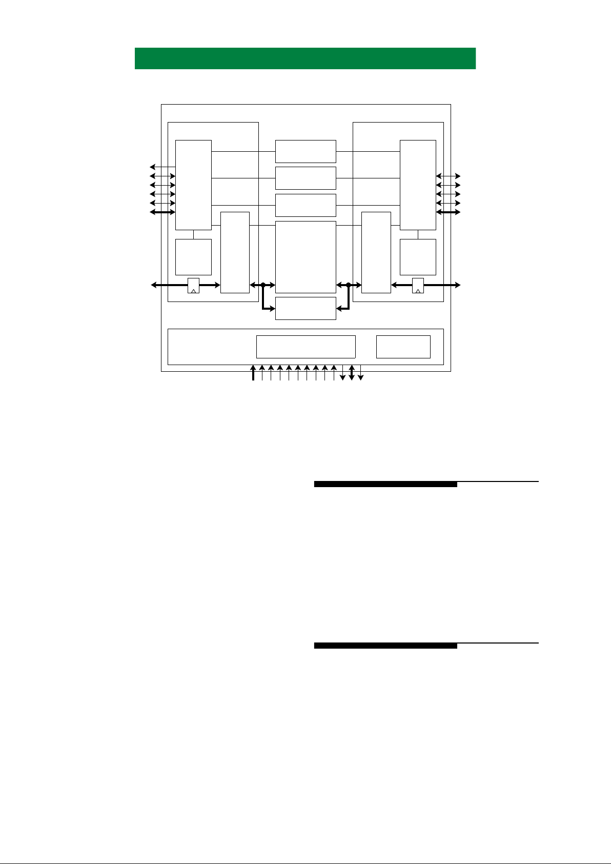
Figure 1: Functional Block Diagram
The Pass Through Controller bloc k allows data
to be transferred bet ween Port A and Port B without
being compressed or decompressed.
Port A and Port B are two independent DMA
interfaces. For compression and decompre ssi on
operations, Port A transf ers uncompressed data and
Port B transfers compre ssed cod es. Each p ort has a
byte counter , which counts the number of bytes that
are transferred through the port. The configuration
of the DMA interface on each po rt is programmable.
These functions incl ude DMA master or slave, eight
or sixteen bit t ransfers, and contr ol pin enabling and
polarity . The Port B Byte Count register has a Port B
Byte Comparator register, allowing the chip to
interrupt after a programmed amount of data has
been transferred on the Port B data bus, DB[15:0].
Register accesses to a peripheral chip connected to
Port A are also supported.
2.0 MODES OF OPERATION
There are two classes of the modes of operatio n
for this chip. The first class is determined by the
Port A and Port B DMA data bus configurations.
Port A and Port B can be dual independent data
buses, or Port A and Port B can be connected to
create a single data bus. The second class is
determined by the method data is processed through
the chip in compression, decompression or pass
through modes.
2.1 PORT A AND B PORT DATA BUS
CONFIGURATION
Port A and Port B data bus configuration is
controlled by the DATA BUS MODE[2:0] bits in
the DMA Configuration regi ster . These bits contro l
the single and dual data bus modes, as well as Port
A and Port B being the DMA bus master or slave
(see Table 1).
PORT A
BYTE
COUNTER
PORT B
BYTE
COUNTER
PORT A
DMA
STATE
MACHINE
PORT A
FIFO
PORT B
DMA
STATE
MACHINE
PORT B
FIFO
SINGLE DATA
BUS ARBITER
RECORD COUNT
REGISTER
RECORD LENGTH
REGISTER
PROCESSOR INTERFACE
STATE MACHINE
PASS THROUGH
CONTROLLER
INTERRUPT
LOGIC
PROCESSOR
INTERFACE
DCLZ
ENGINE
PORT A INTERFACE PORT B INTERFACE
ACSN
DREQA
DACKA
AOE
AWE
DAPTY[1:0]
DA[15:0]
A[4:0]
PORTACSN
CSN
RWN/IOWRN
DSN/IORDN
PROCMODE
TRISTATEN
TEST
RESTN
CLK
DTACKN/READY
D[7:0]
INTN/INT
DREQB
DACKB
BOE
BWE
DBPTY[1:0]
DB[15:0]
(8 Bytes) (8 Bytes)
AHA3210B Compression Chip
Page 8
PS3210B-1299 Page 3 of 45
Advanced Hardware Architectures, Inc.
Table 1: Data Bus Modes
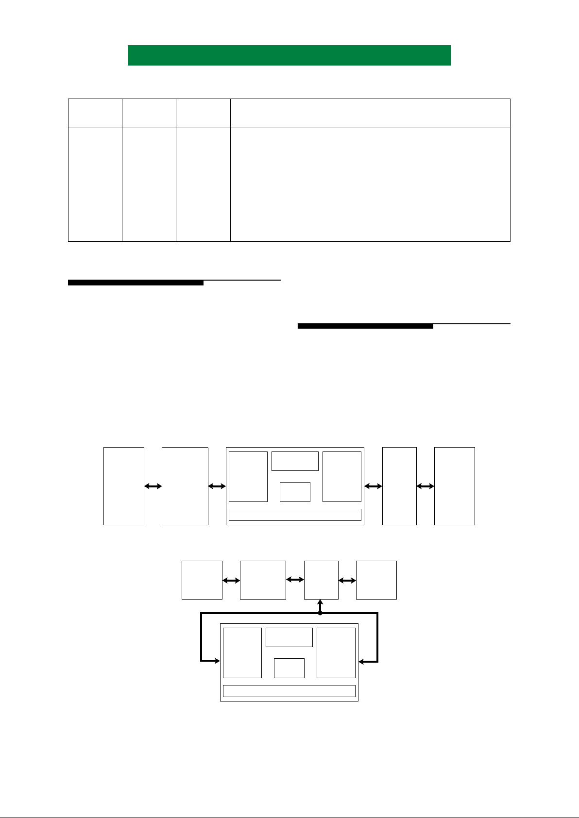
2.1.1 DUAL DATA BUS MODE: IN-LINE
APPLICATION
In dual data bus mode, Port A and Port B
transfer data on unique, independent data buses.
This is used for in-line applications, whe n data is
transferred from th e host interface, t hrough the data
compression coprocessor, and into the system
buffer (see Figure 2).
In dual data bus mode, the data rate during
compression is sustained at 10 MB/sec, except
when the compression ratio is less than 1 (which
occurs briefly when a compression dictionary is
first being built, or when data is actually
expanding). The data rate during decompression,
pass through A to B, a nd pass through B to A modes
is sustained at 10 MBytes/sec (see Figure 3).
2.1.2 SINGLE DATA BUS MODE: LOOK-ASIDE
APPLICATION
In single data bus mode, Port A and Port B
transfer data on a common data bus. This
connection is made external to the chip, on the PC
board. This is used in a look aside application, when
the data compression coproc essor transfers data into
and out of the system buffer.
Figure 2: Dual Data Bus Mode
Figure 3: Single Data Bus Mode
DATA BUS
MODE[2]
DA TA BUS
MODE[1]
DATA BUS
MODE[0]
FUNCTION
0 0 0 Dual data bus: Port B slave, Port A slave
0 0 1 Dual data bus: Port B slave, Port A master
0 1 0 Dual data bus: Port B master, Port A slave
0 1 1 Dual data bus: Port B master, Port A master
1 0 0 Dual data bus: Port B slave, Port A slave with peripheral access
101Reserved
1 1 0 Dual data bus: Port B master, Port A slave with peripheral access
1 1 1 Single data bus: Port B master, Port A master
HOST
INTERFACE
BUS
INTERFACE
PROCESSOR INTERFACE
SYSTEM
TAPE
DRIVE
BUS CONTROLLER
BUFFER
INTERFACE
PORT A
INTERFACE
SINGLE DATA
BUS ARBITER
DCLZ
ENGINE
PORT B
INTERFACE
HOST
INTERFACE
BUS
INTERFACE
PROCESSOR INTERFACE
SYSTEM
TAPE
DRIVE
BUS CONTROLLER
BUFFER
INTERFACE
PORT A
INTERFACE
SINGLE DATA
BUS ARBITER
DCLZ
ENGINE
PORT B
INTERFACE
Page 9
Page 4 of 45 PS3210B-1299
Advanced Hardware Architectures, Inc.
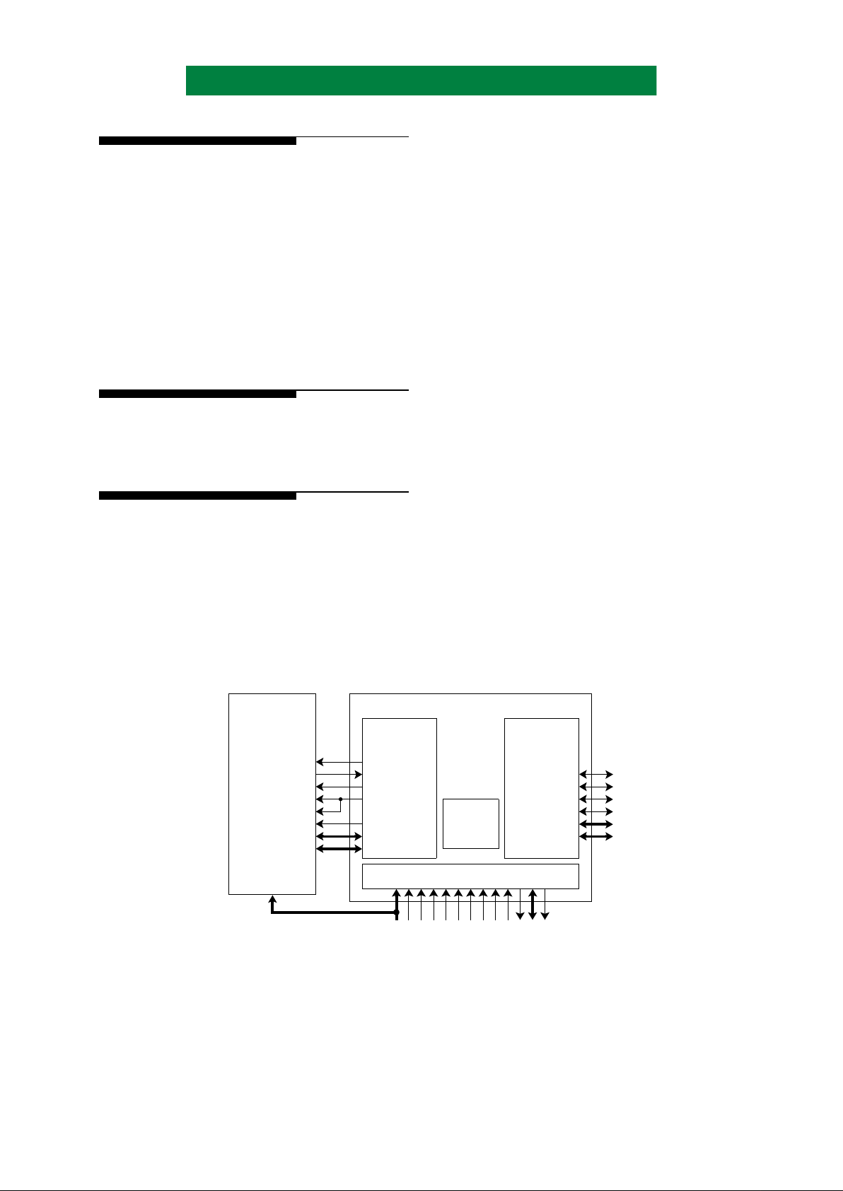
2.1.3 PORT A PERIPHERAL CHIP INTERFACE
A peripheral chip can be connected to Port A,
and have its registers accessed through the
processor interface of the data compression chip
(see Figure 4). This is used in in-line applications,
for peripheral chips with a common DMA and
processor data bus (such as the NCR 53C90A/B and
the NCR 53C94/5/6 SCSI controllers).
It is the firm ware’s responsib ility to ensure
accesses to the peripheral chip’s registers do not
occur while DMA transfers ar e occurring on Port A.
This mode is only s upported when Port A is a DMA
slave, in dual data bus mode.
2.2 DATA PROCESSING MODES
The data processing modes a re controlled by the
DCLZ MODE[2:0] bits in the DCLZ Control
register.
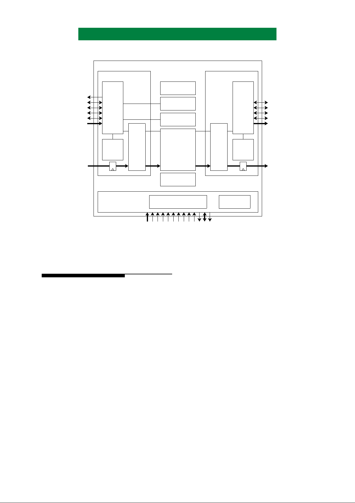
2.2.1 COMPRESSION MODE
During compression mode, uncompres sed data
flows into Port A. It is then comp ressed by the
DCLZ engine. The resulting compressed data is
then transferred out of Port B (see Figure 5).
The uncompressed data i s partitioned into fixed
sized recor ds. The size is stored in the Record
Length register inside the chip. After a record has
been compressed, an end of record codeword is
inserted into the compres sed data. The end of record
codewords are then used during decompression, to
control data flow.
Multiple records can be compressed without
processor intervention. The Record Count register
inside the chip stores the number of records to
compress. A compression sequence has been
completed after the last byte of the last record has
been compressed and transfer red out of Port B. This
event sets the Port B End of Transfer interrupt.
Compression ratio is defined as the number of
uncompressed bytes divided by the number of
compressed bytes. The Port A Byte Counter co unts
the number of uncompressed bytes. The Por t B Byte
Counter counts the number of compressed bytes.
The compression ratio can also be automatically
controlled, by programming the Comp Ratio
Optimization register.
The following sequence is used to p rog ram the
chip to compress multiple, fixed size records:
- Program Record Length register
- Program Record Count register
- Program Interrupt Disable register
- Enable PORT B END OF TRANSFER Interrupt
- Program Comp Ratio Optimization register
- Program DCLZ Control register
DCLZ MODE[2:0] Compression
COMP RATIO OPT ENABLE 1
RESET DICT AFTER EOR 0
RESET DICT 0
PAUSE AFTER EOR 0
PAUSE 0
- The PORT B END OF TRANSFER interrupt signals
compression completed
Figure 4: Port A Peripheral Chip Interface
PROCESSOR INTERFACE
DCLZ
ENGINE
PORT B
CS/
DREQ
DACK/
DBWR/
RD/
DBP[1:0]
DB[15:0]
DREQB
DACKB
BOE
BWE
DBPTY[1:0]
DB[15:0]
INTERFACE
ACSN
DREQA
DACKA
AOE
AWE
DAPTY[1:0]
DA[15:0]
WR/
A[3:0]
PORT A
INTERFACE
PERIPHERAL
A[4:0]
PORTACSN
CSN
RWN/IOWRN
DSN/IORDN
PROCMODE
TRISTATEN
TEST
RESETN
CLK
DTACKN/READY
D[7:0]
INTN/INT
CHIP
AHA3210B Compression Chip
Page 10
PS3210B-1299 Page 5 of 45
Advanced Hardware Architectures, Inc.
Figure 5: Compression Mode
2.2.2 COMPRESSION FLUSH MODE
Normal compression operat ions complete when
the Record Length register and the Record Count
register both decrement to zero. All data in the chip
is then compressed, and transferred out of Port B.
There is no data in the chip, and the chip is said to be
flushed (see Figure 6).
Consider the scenario when a compression
operation is require d to comple te premat urel y (i.e.,
before the Record Length register and the Record
Count register have both decremented to zero). In
this scenario, Port A DMA i s inactive, because there
is no more uncompressed data to transfer into the
chip. Due to the DCLZ data compression algor ithm,
there may be partially compr essed data in the DCLZ
engine at this ti me.
Compression flush mode is used to complete
the compression operation , transfer all compr essed
data out of Port B, and get the chi p into t he flus hed
state. Note that the compression flush operation
inserts an end of recor d code word at the appropriate
location, near the end of the compressed data
stream.
The chip should only be programmed into
compression flus h m od e wh en the Port A Inter fa ce
is empty (i.e., when the Port Inte rface Byte Count in
the Port A Status register is zero) and the DCLZ
engine contains data (i.e., when the DCLZ Engine
Flushed bit in the DCLZ S tatus r egister is zero) and
the DCLZ Engine is not already in the process of
flushing (i.e., The DCLZ EOR COUNT bit in the
DCLZ Status register is zero).
PORT A
BYTE
COUNTER
PORT B
BYTE
COUNTER
PORT A
DMA
STATE
MACHINE
PORT A
FIFO
PORT B
DMA
STATE
MACHINE
PORT B
FIFO
SINGLE DATA
BUS ARBITER
RECORD COUNT
REGISTER
RECORD LENGTH
REGISTER
PROCESSOR INTERFACE
STATE MACHINE
PASS THROUGH
CONTROLLER
INTERRUPT
LOGIC
PROCESSOR
INTERFACE
DCLZ
ENGINE
PORT A INTERFACE PORT B INTERFACE
ACSN
DREQA
DACKA
AOE
AWE
DAPTY[1:0]
DA[15:0]
A[4:0]
PORTACSN
CSN
RWN/IOWRN
DSN/IORDN
PROCMODE
TRISTATEN
TEST
RESTN
CLK
DTACKN/READY
D[7:0]
INTN/INT
DREQB
DACKB
BOE
BWE
DBPTY[1:0]
DB[15:0]
(8 Bytes) (8 Bytes)
AHA3210B Compression Chip
Page 11
Page 6 of 45 PS3210B-1299
Advanced Hardware Architectures, Inc.
The following sequence is use d to prog ram the
chip for Compression Flush mode for the scenario
described above:
- Program DCLZ Control register
DCLZ MODE[2:0] Compression
COMP RATIO OPT ENABLE 1
RESET DICT AFTER EOR 0
RESET DICT 0
PAUSE AFTER EOR 0
PAUSE 1
- Wait until the PAUSED bit in the DCLZ Status register is set
- Program Record Count register to 000000 hex
- Program Interrupt Disable register
- Enable PORT B END OF TRANSFER Interrupt
- If the DCLZ Engine Flushed bit is zero and the DCLZ EOR
COUNT bit is zero, then there is data in the DCLZ Engine to
transfer out via compression flush mode.
BEGIN
- Program DCLZ Control register
DCLZ MODE[2:0] Compression flush
COMP RATIO OPT ENABLE 1
RESET DICT AFTER EOR 0
RESET DICT 0
PAUSE AFTER EOR 0
PAUSE 0
- The PORT B END OF TRANSFER interrupt signals
compression completed
END
- If the DCLZ Engine Flushed bit is zero and the DCLZ EOR
COUNT bit is one, then the DCLZ Engine is already in the
process of flushing.
BEGIN
- Program DCLZ Control register
DCLZ MODE[2:0] Compression
COMP RATIO OPT ENABLE 1
RESET DICT AFTER EOR 0
RESET DICT 0
PAUSE AFTER EOR 0
PAUSE 0
- The PORT B END OF TRANSFER interrupt signals
compression completed
END
- If the DCLZ Engine Flushed bit is one and the Port B Interface
Byte Count is not zero, then there is data in the Port B Interface
to transfer out.
BEGIN
- Program DCLZ Control register
DCLZ MODE[2:0] Compression
COMP RATIO OPT ENABLE 1
RESET DICT AFTER EOR 0
RESET DICT 0
PAUSE AFTER EOR 0
PAUSE 0
- The PORT B END OF TRANSFER interrupt signals
compression completed
END
- If the DCLZ Engine Flushed bit is one and the Port B Interface
Byte Count is zero, then the DCLZ Engine and the Port B
Interface are already flushed.
Figure 6: Compression Flush Mode
PORT A
BYTE
COUNTER
PORT B
BYTE
COUNTER
PORT A
DMA
STATE
MACHINE
PORT A
FIFO
PORT B
DMA
STATE
MACHINE
PORT B
FIFO
SINGLE DATA
BUS ARBITER
RECORD COUNT
REGISTER
RECORD LENGTH
REGISTER
PROCESSOR INTERFACE
STATE MACHINE
PASS THROUGH
CONTROLLER
INTERRUPT
LOGIC
PROCESSOR
INTERFACE
DCLZ
ENGINE
PORT A INTERFACE PORT B INTERFACE
ACSN
DREQA
DACKA
AOE
AWE
DAPTY[1:0]
DA[15:0]
A[4:0]
PORTACSN
CSN
RWN/IOWRN
DSN/IORDN
PROCMODE
TRISTATEN
TEST
RESTN
CLK
DTACKN/READY
D[7:0]
INTN/INT
DREQB
DACKB
BOE
BWE
DBPTY[1:0]
DB[15:0]
(8 Bytes) (8 Bytes)
AHA3210B Compression Chip
Page 12
PS3210B-1299 Page 7 of 45
Advanced Hardware Architectures, Inc.
2.2.3 DECOMPRESSION MODE
During decompression mode, compressed data
flows into Port B. It is then uncompressed by the
DCLZ engine. The resulting uncompressed data is
then transferred out of Port A.
The compressed data is partitioned into records,
with End of Record codewords embedded in the
compressed data. Multiple records can be
automatically decompressed, by programming the
number of records into the Record Coun t register . A
decompression sequence has been completed after
the last byte of the last record has been
uncompressed and then transferred out of Port A.
This event sets the Port A End of T r ansfer int errupt.
The following sequence is used to p rogram the
chip to decompress multiple records:
- Program Record Count register
- Program Interrupt Disable register
- Enable PORT A END OF TRANSFER Interrupt
- Program DCLZ Control register
DCLZ MODE[2:0] Decompression
COMP RATIO OPT ENABLE 0
RESET DICT AFTER EOR 0
RESET DICT 0
PAUSE AFTER EOR 0
PAUSE 0
- The PORT A END OF TRANSFER Interrupt signals
decompression completed
Figure 7: Decompression Mode
PORT A
BYTE
COUNTER
PORT B
BYTE
COUNTER
PORT A
DMA
STATE
MACHINE
PORT A
FIFO
PORT B
DMA
STATE
MACHINE
PORT B
FIFO
SINGLE DATA
BUS ARBITER
RECORD COUNT
REGISTER
RECORD LENGTH
REGISTER
PROCESSOR INTERFACE
STATE MACHINE
PASS THROUGH
CONTROLLER
INTERRUPT
LOGIC
PROCESSOR
INTERFACE
DCLZ
ENGINE
PORT A INTERFACE PORT B INTERFACE
ACSN
DREQA
DACKA
AOE
AWE
DAPTY[1:0]
DA[15:0]
A[4:0]
PORTA CSN
CSN
RWN/IOWRN
DSN/IORDN
PROCMODE
TRISTATEN
TEST
RESTN
CLK
DTACKN/READY
D[7:0]
INTN/INT
DREQB
DACKB
BOE
BWE
DBPTY[1:0]
DB[15:0]
(8 Bytes) (8 Bytes)
AHA3210B Compression Chip
Page 13
Page 8 of 45 PS3210B-1299
Advanced Hardware Architectures, Inc.
2.2.4 DECOMPRESSION OUTPUT DISABLED
MODE
The DCLZ algorithm allows the compression
dictionary to be shared between multiple records.
To decompress records in the middle of a multiple
record sequence, the pr eceding records must first be
decompressed, in order to properly build the
compression dictionary.
Decompression output disabled mode allows
the preceding records to be decompressed, while
discarding the unwanted un compr essed data. Once
this is completed, the chip can be programmed to
decompression mode, to decompr ess and output the
desired records.
In decompression output disabled mode, the
data is discarded between the Port A Interface and
the Port A pins. Port A DMA remains inactive . The
Port B Byte Counter, the Port A Byte Counter, the
Port B Interface Byte Count, the Port A Interface
Byte Count, the Record Count regis ter , and the Port
A End of Transfer Interrupt operate as in
decompression mode. It is recommended that the
Port A Interface be empty and th e chip paused
before switching between decompression output
disabled and decompression modes.
The following sequence is used to p rog ram the
chip to decompress multiple records in output
disabled mode:
- Program Record Count register
- Program Interrupt Disable register
- Enable PORT A END OF TRANSFER Interrupt
- Program DCLZ Control register
DCLZ MODE[2:0] Decomp; Output
Disabled Mode
COMP RATIO OPT ENABLE 0
RESET DICT AFTER EOR 0
RESET DICT 0
PAUSE AFTER EOR 0
PAUSE 0
- The PORT A END OF TRANSFER Interrupt signals
decompression output disabled completed
Figure 8: Decompression Output Disabled Mode
PORT A
BYTE
COUNTER
PORT B
BYTE
COUNTER
PORT A
DMA
STATE
MACHINE
PORT A
FIFO
PORT B
DMA
STATE
MACHINE
PORT B
FIFO
SINGLE DATA
BUS ARBITER
RECORD COUNT
REGISTER
RECORD LENGTH
REGISTER
PROCESSOR INTERFACE
STATE MACHINE
PASS THROUGH
CONTROLLER
INTERRUPT
LOGIC
PROCESSOR
INTERFACE
DCLZ
ENGINE
PORT A INTERFACE PORT B INTERFACE
ACSN
DREQA
DACKA
AOE
AWE
DAPTY[1:0]
DA[15:0]
A[4:0]
PORTA CSN
CSN
RWN/IOWRN
DSN/IORDN
PROCMODE
TRISTATEN
TEST
RESTN
CLK
DTACKN/READY
D[7:0]
INTN/INT
DREQB
DACKB
BOE
BWE
DBPTY[1:0]
DB[15:0]
(8 Bytes) (8 Bytes)
AHA3210B Compression Chip
Page 14
PS3210B-1299 Page 9 of 45
Advanced Hardware Architectures, Inc.
2.2.5 PASS THROUGH A TO B MODE
During pass through A to B mode, data enters
Port A, is transferred through the Port A Interface
and the Port B Interface, and then transferred out of
Port B. The data is not altered as it passes through
the chip.
The Record Le ngth register determines the
number of bytes in a record. The Record Count
register determines the number of records. Multiply
the values of these two registers to determine the
total number of bytes that will be transferred
through the chip. The pass through sequence has
been completed after the last byte of the last record
has been transferred out of Port B. This event sets
the Port B End of Transfer interrupt.
The following sequence is used to p rogram the
chip to pass through data from Port A to Port B:
- Program Record Length register
- Program Record Count register
- Program Interrupt Disable register
- Enable PORT B END OF TRANSFER Interrupt
- Program DCLZ Control register
DCLZ MODE[2:0] Pass through A to B
COMP RATIO OPT ENABLE 0
RESET DICT AFTER EOR 0
RESET DICT 0
PAUSE AFTER EOR 0
PAUSE 0
- The PORT B END OF TRANSFER interrupt signals pass
through A to B completed
Figure 9: Pass Through A to B Mode
PORT A
BYTE
COUNTER
PORT B
BYTE
COUNTER
PORT A
DMA
STATE
MACHINE
PORT A
FIFO
PORT B
DMA
STATE
MACHINE
PORT B
FIFO
SINGLE DATA
BUS ARBITER
RECORD COUNT
REGISTER
RECORD LENGTH
REGISTER
PROCESSOR INTERFACE
STATE MACHINE
PASS THROUGH
CONTROLLER
INTERRUPT
LOGIC
PROCESSOR
INTERFACE
DCLZ
ENGINE
PORT A INTERFACE PORT B INTERFACE
ACSN
DREQA
DACKA
AOE
AWE
DAPTY[1:0]
DA[15:0]
A[4:0]
PORTACSN
CSN
RWN/IOWRN
DSN/IORDN
PROCMODE
TRISTATEN
TEST
RESTN
CLK
DTACKN/READY
D[7:0]
INTN/INT
DREQB
DACKB
BOE
BWE
DBPTY[1:0]
DB[15:0]
(8 Bytes) (8 Bytes)
AHA3210B Compression Chip
Page 15

Page 10 of 45 PS3210B-1299
Advanced Hardware Architectures, Inc.
2.2.6 PASS THROUGH B TO A MODE
During pass through B to A mode, data enters
Port B, is transferred through the Port B Interface
and Port A In terface, and is then transferred out of
Port A. The data is not altered as it passes through
the chip.
The Record Le ngth register determines the
number of bytes in a record. The Record Count
register determines the number of records. Multiply
the values of these two registers to determine the
total number of bytes that will be transferred
through the chip. The pass through sequence has
been completed after the last byte of the last record
has been transferred out of Port A. This event sets
the Port A End of Transfer interrupt.
The following sequence is used to p rogram the
chip to pass through data from Port B to Port A:
- Program Record Length register
- Program Record Count register
- Program Interrupt Disable register
- Enable PORT A END OF TRANSFER Interrupt
- Program DCLZ Control register
DCLZ MODE[2:0] Pass through B to A
COMP RATIO OPT ENABLE 0
RESET DICT AFTER EOR 0
RESET DICT 0
PAUSE AFTER EOR 0
PAUSE 0
- The PORT A END OF TRANSFER interrupt signals pass
through B to A completed
Figure 10: Pass Through B to A Mode
PORT A
BYTE
COUNTER
PORT B
BYTE
COUNTER
PORT A
DMA
STATE
MACHINE
PORT A
FIFO
PORT B
DMA
STATE
MACHINE
PORT B
FIFO
SINGLE DATA
BUS ARBITER
RECORD COUNT
REGISTER
RECORD LENGTH
REGISTER
PROCESSOR INTERFACE
STATE MACHINE
PASS THROUGH
CONTROLLER
INTERRUPT
LOGIC
PROCESSOR
INTERFACE
DCLZ
ENGINE
PORT A INTERFACE PORT B INTERFACE
ACSN
DREQA
DACKA
AOE
AWE
DAPTY[1:0]
DA[15:0]
A[4:0]
PORTACSN
CSN
RWN/IOWRN
DSN/IORDN
PROCMODE
TRISTATEN
TEST
RESTN
CLK
DTACKN/READY
D[7:0]
INTN/INT
DREQB
DACKB
BOE
BWE
DBPTY[1:0]
DB[15:0]
(8 Bytes) (8 Bytes)
AHA3210B Compression Chip
Page 16

PS3210B-1299 Page 11 of 45
Advanced Hardware Architectures, Inc.
3.0 REGISTER DESCRIPTION
Table 2: Register Address Map
Notations:
* These registers have one or more reserved bits set to ‘0’. These registers read back ‘0’ from these reserved bits.
** A soft reset is generated by writing a reset command to DCLZ MODE[2:0].
U - These bits remain unchanged after a soft reset.
x - Indicates undefined bit.
ADDRESS READ WRITE
HARD
RESET
SOFT**
RESET
0x00 DCLZ Control DCLZ Control 1110,0000 111U,UUUU
0x01 DCLZ Status Reserved 0000,0011 0000,0011
0x02 Comp Ratio Optimization Comp Ratio Optimization 0000,0000 Unchanged
0x03 *DMA Configuration DMA Configuration 0000,0101 Unchanged
0x04 Port A Control 0 Port A Control 0 0000,0000 Unchanged
0x05 *Port A Control 1 Port A Control 1 x000,00xx Unchanged
0x06 Port A Status Reserved 0000,0000 0U00,0000
0x07 Port A Byte Count [7:0] Port A Byte Count [7:0] 0000,0000 Unchanged
0x08 Port A Byte Count [15:8] Port A Byte Count [15:8] 0000,0000 Unchanged
0x09 Port A Byte Count [23:16] Port A Byte Count [23:16] 0000,0000 Unchanged
0x0A Port B Control 0 Port B Control 0 0000,0000 Unchanged
0x0B *Port B Control 1 Port B Control 1 x000,00xx Unchanged
0x0C Port B Status Reserved 0000,0000 0U00,0000
0x0D Port B Byte Count [7:0] Port B Byte Count [7:0] 0000,0000 Unchanged
0x0E Port B Byte Count [15:8] Port B Byte Count [15:8] 0000,0000 Unchanged
0x0F Port B Byte Count [23:16] Port B Byte Count [23:16] 0000,0000 Unchanged
0x10 Port B Byte Comparator [7:0] Port B Byte Comparator [7:0] Undefined Unchanged
0x11 Port B Byte Comparator [15:8] Port B Byte Comparator [15:8] Undefined Unchanged
0x12 Port B Byte Comparator [23:16] Port B Byte Comparator [23:16] Undefined Unchanged
0x13 Record Length [7:0] Record Length [7:0] Undefined Unchanged
0x14 Record Length [15:8] Record Length [15:8] Undefined Unchanged
0x15 Record Length [23:16] Record Length [23:16] Undefined Unchanged
0x16 Record Count [7:0] Record Count [7:0] Undefined Unchanged
0x17 Record Count [15:8] Record Count [15:8] Undefined Unchanged
0x18 Record Count [23:16] Record Count [23:16] Undefined Unchanged
0x19 Interrupt Stat us Interr upt Clear 0000,0000 Unchanged
0x1A *Interrupt Disable Interrupt Disable 0011,1111 Unchanged
0x1F Identification Reserved 0100,0001 0100,0001
Page 17

Page 12 of 45 PS3210B-1299
Advanced Hardware Architectures, Inc.
3.1 DCLZ CONTROL: ADDRESS 00 HEX - READ/WRITE
DCLZ MODE[2 :0] = DCLZ Control r egister [7:5]:
The DCLZ MODE bits determine how the chip will process data as follows.
– Pass through modes transfer data through the chip without any compression or decompression
operation. Pass through A to B transfers data into Port A and out of Port B. Pass through B to A
transfers data into Port B and out of Port A.
– Compression mode transfers uncompressed data into Port A, compresses it, and transfers
compressed data out of Port B.
– Compression flush mode causes all data in the DCLZ Engine to be compr essed inc luding an end of
record codeword, and then flushed out of the chip through Port B.
– Decompression mode transfers compressed data into Port B, decompresses it, and transfers
uncompressed data out of Port A.
– Decompression output disabled mode transfers compressed data into Port B, decompresses it and
builds the decompression dictionary, but does not transfer any uncompressed data out of Port A.
– Reset mode resets all state machines and data in Port A, Port B, single data bus arbiter, and the
DCLZ engine. It also resets the dictionary. It resets the registers as shown in Table 2.
The DCLZ Control bits should always be programmed to the reset mode, when switching between all
modes, except between compression and compression flush modes and between decompression and
decompression output disabled modes. It is recommended that the Port A Interface be empty and the
chip paused before switching between decompression output disabled and decompression modes. The
DCLZ MODE bits are set to on e when the chip is rese t from the RESETN pin. The DCLZ MODE bits
are decoded as shown below:
Table 3: DCLZ Mode Bit Decode
COMP RATIO OPT ENABLE:
The COMPRESSION RATIO OPTIMIZATION ENABLE bit enables the automatic compression ratio
optimizer during compression. This bit enables the THRESH[5:0] and PERIOD[1:0] bits in the Comp
Ratio Optimization register. A one enables optimization, and a zero disables optimization. This bit is
cleared to zero when the chip is reset from the RESETN pin.
RESET DICT AFTER EOR:
During compression, the RESET DICTIONARY AFTER END OF RECORD bit causes the DCLZ
engine to reset the compr ession dicti onary after each end of record, and before the fi rst subsequent byt e
which is not designated as an end of record. A one resets the dictionary after end of record, and a zero
has no effect on the di ction ary. This bit is cleared to zero when the chip is rese t from the RESETN pin.
bit7 bit6 bit5 bit4 bit3 bit2 bit1 bit0
0x00 D C L Z M O DE[2:0]
COMP
RATIO OPT
ENABLE
RESET DICT
AFTER EOR
RESET
DICT
PAUSE
AFTER EOR
PAUSE
DCLZ
MODE[2]
DCLZ
MODE[1]
DCLZ
MODE[0]
FUNCTION
0 0 0 Pass through A to B
0 0 1 Pass through B to A
010Compression
0 1 1 Compression flush
1 0 0 Decompression
1 0 1 Decompression output disable
110Reserved
111Reset
Page 18

PS3210B-1299 Page 13 of 45
Advanced Hardware Architectures, Inc.
RESET DICT
The RESET DICTIONARY bit causes the compression dictionary to be reset after completing the
current byte, and before the next byte which is not designated as an end of record. A one causes the
dictionary to be reset, and a zero has no effect on the dictionary. The RESET DICT bit will be
automatically cleared, once a dictionary rese t has occurred. This bit is c le are d to zer o when t h e ch ip i s
reset from the RESETN pin.
PAUSE AFTER EOR:
Writing a one to the PAUSE AFTER END OF RECORD bit causes the Port A interface, the DCLZ
Engine and the Port B interface to pause after each end of record has been processed. The PA USED
status bit in the DCLZ Status register is then set. To allow the chip to continue, a zero must be written
to the PAUSE bit. This bit is cleared to zero when the chip is reset from the RESETN pin.
PAUSE:
Writi ng a one to the PAUSE bit causes the Port A interface, the DCLZ Engine, and the Port B interface
to pause. The PAUSED status bit in the DCLZ Status regist er i s then set. Writ ing a zero to the PAUSE
bit allows the chip to resume operation after it has been paused or paused after end of record. PAUSE
bit operation is suppor ted during processor write cyc les which program the DCLZ Control bit s out of the
Reset state. This bit is cleared to zero when the chip is reset from the RESETN pin.
Table 4: Supported Modes for DCLZ Control Register Bits
3.2 DCLZ STATUS: ADDRESS 01 HEX - READ ONLY
res - Reserved. Bits read back zeros.
DCLZ EOR COUNT:
The DCLZ EOR COUNT bit shows the number of end of records contai ned in the DCLZ Engi ne. This
bit operates in compression, compression flush, decompression, and decompression output disabled
mode. This bit is cleared to zero when the reset or pass through A to B or pass through B to A code is
programmed to the DCLZ MODE bits in the DCLZ Control register, or when the chip is reset by the
RESETN pin. The DCLZ EOR COUNT bit can transition frequently when the DCLZ Engine is actively
processing data (i.e., when it is not paused). Therefore, the DCLZ EOR COUNT bit should only be
considered valid when the PAUSED bit is one.
DCLZ ENGINE FLUSHED:
This bit operates in compression, compression flush, decompression, and decompression output
disabled modes only. When the DCLZ ENGINE FLUSHED bit is a one, there is no data in the DCLZ
Engine. This occurs a fter an end of record has bee n processed thr ough the DCLZ Engine , and before the
first byte of t he n ext r ecord has entered t he DCLZ Engine. Once the first byte of the next re cor d e n te rs
the DCLZ Engine, the DCLZ ENGINE FLUSHED bit is cleared to zero. The DCLZ ENGINE
FLUSHED bit is set to one when the DCLZ MODE bits are programmed to pass through A to B, pass
through B to A, or reset mode. Also, the DCLZ ENGINE FLUSHED bit is set to one when the chip is
reset by the RESETN pin. The DCLZ ENGINE FLUSHED bit can transi tion frequently when the DCLZ
Engine is actively processing data (i.e., when it is not paused). Therefore, the DCLZ ENGINE
FLUSHED bit should only be considered valid when the PAUSED bit is one.
MODE
COMP RATIO
OPT ENABLE
RESET DICT
AFTER EOR
RESET
DICT
PAUSE
AFTER EOR
PAUSE
Compression YES YES YES YES YES
Compression flush YES YES YES YES YES
Decompression NO NO NO YES YES
Decompression output disabled NO NO NO YES YES
Pass through A to B NO NO NO YES YES
Pass through B to A NO NO NO YES YES
bit7 bit6 bit5 bit4 bit3 bit2 bit1 bit0
0x01 res
DCLZ EOR
COUNT
DCLZ ENGINE
FLUSHED
P AUSED
Page 19

Page 14 of 45 PS3210B-1299
Advanced Hardware Architectures, Inc.
PAUSED:
When the PAUSED bit is one, the Port A interface, the DCLZ Engine, and the Port B interface ar e
paused. The Port A By te Cou nt regi sters, t he Port B Byte Co unt regist ers, th e Port A S tatus r egister, the
Port B Statu s register , the Record Lengt h registers, and the Record Count reg isters are stable at this time.
This bit is set to one when the chip is reset from the RESETN pin, or when the DCLZ Control bits are
programmed to the Reset state.
3.3 COMP RATIO OPTIMIZATION: ADDRESS 02 HEX - READ/WRITE
This register is used to control the compression ratio during compression mode, by automatically
resetting the compression dictionary if the compression ratio is below the programmed threshold. If the
compression dictionary is less than half full the optimization circuit will check the compression ratio and
compare it to the compression ratio programmed in the THRESHOLD parameter every 1024 input bytes
and reset the dictionary if the compression ratio does not meet or exceed this value. After the dictionary is
greater than half full, the optim izer will check the compression ratio against a threshold every n bytes ,
where n is determined by the value of the PERIOD bits. The threshold is set by the value of the THRESH
bits. Optimization is enabled by setting COMP RATIO OPT ENABLE bit in the DCLZ Control register.
The compression ratio is specified by the thresh old bits according to the following formula:
For example, if THRESH is set at 32 the com pression ratio is 2. This compression ratio i s a target. After
every N number of bytes as specified by the PERIOD field has been input, the actual compression ratio is
checked against the target. If the actual is less than the target, the dictionary is automatically reset. The
THRESH[5:0] and PERIOD[1:0] bits are zero when the chip is reset by the RESETN pin.
3.4 DMA CONFIGURATION: ADDRESS 03 HEX - READ/WRITE
res - Reserved. Bits must always be written with zeros. They read back zeros.
DATA BUS MODE [2:0]:
The DA TA BUS MODE bits determine the data configuration for the Port A and Port B DMA buses. In
dual data bus mode, Port A and Por t B are indepe nde nt, isolat ed data buses. Dat a tra nsfer s on each b us
may occur simultane ously . In this mode, Port A and Port B can b e any combination of DMA bus masters
or slaves. This mode is intend ed for in lin e applicatio ns. In sing le bus mode, the Por t A and Port B data
buses are connected together on the PC board.
bit7 bit6 bit5 bit4 bit3 bit2 bit1 bit0
0x02
THRESH[5:0] PERIOD[1:0]
PERIOD
bit 1 bit 0 Size
0 0 512 bytes
0 1 1024 bytes
1 0 2048 bytes
1 1 4096 bytes
COMPRESSION RANGES
Compression Ratio Threshold Value
1 → 20 → 32
2 → 333 → 42
3 → 443 → 48
4 → 849 → 56
8 → 64 57 → 63
bit7 bit6 bit5 bit4 bit3 bit2 bit1 bit0
0x03 res
DATA BUS MODE[2:0]
compression ratio
64
64 THRESH–
-----------------------------------=
Page 20

PS3210B-1299 Page 15 of 45
Advanced Hardware Architectures, Inc.
Both Port A and Port B are DMA bus masters. The Single Data Bus Arbiter circuit inside the chip
resolves all bus con tention on thi s si ngle d ata bu s. Port A and Port B will never simul taneous ly r equest
the data bus in this mode. This mode i s intended for l ook aside app lications. No te that in s ingle data bus
mode, the DMA port which is transfer ring data out of t he chip has pri ority over the DMA port which is
transferring data into the chip.
The Port A interface suppo rts re gister a ccesse s to a per ipher al chi p on the Por t A data b us. regi ster and
DMA accesses between the Po rt A interface and the per ipheral chip occur on a si ngle data bus, DA[7:0].
This mode is only supported when Port A is a DMA slave in dual data bus mode.
Data bus mode bits are set to 101 after the chip is reset by RESETN.
Table 5: DATA BUS MODE Bit Decode
The Port A and Port B DMA control pins change direction, based on the master or slave mode. The
following table shows the DMA control pin direction for DMA bus master and slave modes: Port A
DMA Bus Master/Slave Pin Configuration
Table 6: Port A DMA Bus Master/Slave Pin Configuration
Table 7: Port B DMA Bus Master/Slave Pin Configuration
3.5 PORT A CONTROL 0: ADDRESS 04 HEX - READ/WRITE
ENABLE DA PULLUP:
A one enables the pullups on the DA[15 :0] pins . A zero tri states the pull ups on th e DA[15:0] pins. This
bit is cleared to zero when the chip is reset by the RESETN pin.
DATA BUS
MODE[2]
DA TA BUS
MODE[1]
DATA BUS
MODE[0]
FUNCTION
0 0 0 Dual data bus: Port B slave, Port A slave
0 0 1 Dual data bus: Port B slave, Port A master
0 1 0 Dual data bus: Port B master, Port A slave
0 1 1 Dual data bus: Port B master, Port A master
1 0 0 Dual data bus: Port B slave, Port A slave with peripheral access
101Reserved
1 1 0 Dual data bus: Port B master, Port A slave with peripheral access
1 1 1 Single data bus: Port B master, Port A master
PIN NAME
PORT A DMA
BUS MASTER
PORT A DMA
BUS SLAVE
DREQA Output Input
DACKA Input Output
AOE Input Output
AW E Input Output
PIN NAME
PORT B DMA
BUS MASTER
PORT B DMA
BUS SLAVE
DREQB Output Input
DACKB Input Output
BOE Input Output
BWE Input Output
bit7 bit6 bit5 bit4 bit3 bit2 bit1 bit0
0x04
ENABLE
DA
PULLUP
ENABLE
DAPTY
PULLUP
AWE
ENABLE
AOE
ENABLE
AWE
POLARITY
AOE
POLARITY
DREQA
POLARITY
DACKA
POLARITY
Page 21

Page 16 of 45 PS3210B-1299
Advanced Hardware Architectures, Inc.
ENABLE DAPTY PULLUP:
A one enables the pullups on th e DAPTY[1 :0] pins. A zero tristates the pullups on the DAP TY[1:0] pins.
This bit is cleared to zero when the chip is reset by the RESETN pin.
AWE ENABLE:
A one enables the A WE input when Port A is a DMA bus master , and enables the A WE output when Port
A is a DMA bus sl ave. A zero disables t he AWE input when Port A is a DMA bus master, and tristates
the AWE output when Port A is a DMA bus slave. This bit is cleared to zero when the chip is reset by
the RESETN pin.
AOE ENABLE:
A one enables the AOE input when Port A is a DMA bus master , and enables t he AOE output when Port
A is a DMA bus slave. A zero disable s t he AOE i nput when Port A is a DMA bus master, and tristates
the AOE output when Port A is a DMA bus slave. This bit is cleared to zero when the chip is reset by
the RESETN pin.
AWE POLARITY:
A one makes AWE high active. A zero makes A WE low active. This bit is cleared to zero when the chip
is reset by the RESETN pin.
AOE POLARITY:
A one makes AOE high active. A zer o makes AOE low act ive. This bit is cl eared to z ero when the chip
is reset by the RESETN pin.
DREQA POLARITY:
A one makes DREQA high active. A zero makes DREQA low active. This bit is cleared to zero when
the chip is reset by the RESETN pin.
DACKA POLARITY:
A one makes DACKA high active. A z ero makes DACKA low active. This bit is cl ear ed to zero when
the chip is reset by the RESETN pin.
3.6 PORT A CONTROL 1: ADDRESS 05 HEX - READ/WRITE
DATA BUS WIDTH:
A one makes the Port A data bus 16 bi ts wide, with data transf erred on the DA[15:0] p ins. A zero makes
the Port A data bus 8 bits wide, with data transferred on the DA[7:0] pins. This bit should only be
changed afte r the reset code ha s been programmed to the DCLZ Control bits in the DCLZ Control
register. This bit is undefined when the chip is reset from the RESETN pin.
DATA15TO8:
The DATA 15TO8 bi t causes on e byte to be t ransferred on DA[15:8] on t he next DMA cycle i nto or out
of Port A, when Port A is in 16 bit mode. The intended use of this bit is to transfer a single byte on
DA[15:8] only during t he first DMA cycl e of a contiguo us data transfer sequence. The DATA15T O8 bit
only functions when Port A is in 16 bit mode, and is ignored when Port A is in 8 bit mode. The
DATA15TO8 bit should only be changed after the reset code has been programmed into the DCLZ
Control bits in the DCLZ Control register, or after the chip has paused after end of record, or after the
chip has paused be cause the Port A or Por t B end of transf er inter rupt has occurred . DATA15TO8 ta kes
effect only on the next DMA cycle, which is defin ed as the next occurrence when DACKA pulses active,
and is supported when Port A is a DMA bus master or a DMA bus slave. After the DMA cycle occurs,
the DA TA15TO8 bit is automa tically cleared. DATA15TO8 i s cleared to zero when the chi p is reset from
the RESETN pin.
res - Reserved. Bit must always be written with a zero. It reads back a zero.
bit7 bit6 bit5 bit4 bit3 bit2 bit1 bit0
0x05
DAT A
BUS
WIDTH
DATA15TO8
res
PORT A
DISABLE
CLEAR
INTERF ACE
CLEAR
BYTE
COUNTER
ENABLE
PARITY
ODD
PARITY
Page 22

PS3210B-1299 Page 17 of 45
Advanced Hardware Architectures, Inc.
PORT A DISABLE:
A one disables the Port A control and data buses. The Port A output control signals are made hi-
impedance. The Port A inp ut con trol signa ls ar e ig nored. The DA[15 :0] a nd DAPTY[1:0] data pins are
put into a hi-impeda nce sta te and any tr ansit ions on them are i gnored . A zero in t his bi t posi tion pl aces
Port A into normal operatio nal mode. This bit should only be cha nged while the chip is paus ed at an End
of Transfe r condition. The co ntents of the DCLZ Cont rol register , t he DMA Configuration r egister , and
the Port A Control 0 register, should not be changed while this bit is a one. This bit is cleared to zero
when the chip is reset from the RESETN pin.
CLEAR INTERFACE:
Writi ng a one crea tes a pul se, which clears the Port A Interf ace. W r iting a zero has no ef fect on the Port
A Interface. This bit is always a zero when it is read. The CLEAR INTERF ACE bit is int ended to be used
only when the chip has paused after end of record, or paused becaus e the Port A or Port B end of transf er
interrupt has occurred.
CLEAR BYTE COUNTER:
Writi ng a one crea tes a puls e, which cle ars the Port A Byte Count regi ster. Writing a zero has no ef fect
on the Port A Byte Count register. This bit is always a zero when it is read.
ENABLE PARITY:
A one enables parity on DAPTY[1:0] when Port A is in 16 bit mode, and on DAPTY[0] when Port A is
in 8 bit mode. W riting a zero disables parity on Port A. This bit is undefined when the chi p is reset fro m
the RESETN pin.
ODD PARITY:
A one selects odd parit y on Port A. A ze ro select s even par ity on Port A. This bit i s undefined whe n the
chip is reset from the RESETN pin.
3.7 PORT A STATUS: ADDRESS 06 HEX - READ ONLY
res - Reserved. Bit reads back zero.
DATA7TO0:
When Port A is in 16 bit mode, the DATA7T O0 bit shows whet her the l ast DMA cycle o f a data transf er
sequence out of Port A contains one or two valid bytes. This occurs for the last byte of the last record,
as determined by the Record Count register. If the last byte of the last record is the first byte in the
sequence to output a word, that byte is output on DA[7:0], the data on DA[15:8] is undefined, and the
DATA7TO0 bit is set. If the last byte of the last record is the second byte in the sequence to output a
word, the second to last byte is output on DA[7:0], the last byte is output on DA[15:8], and the
DATA7 TO0 bi t is clear ed. The DATA7T O0 bit is cleared during al l DMA cycles into Port A, during a ll
DMA cycles when Port A is in 8 bit mode, and when the chip is reset from the RESETN pin.
EOR COUNT[1:0]:
The EOR COUNT[1:0] bits show the number of bytes wit h act iv e end of record flags contained in the
Port A Interface. These bits operate in compression, compressi on flush, decompres sion, decompression
output disabled, pass through A to B, and pass throu gh B to A modes. These bits are c leared to zero when
a one is written to the CLEAR INTERFACE bit in Port A Control 1 register, or when the reset code is
programmed to the DCLZ MODE bits in the DCLZ Control register, or when the chip is reset by the
RESETN pin. During data transfers, the se bits should onl y be read when the PAUSED bit in the DCLZ
Status register is a one.
INTERFACE BYTE COUNT[3:0]:
The INTERFACE BYTE COUNT[3:0] bits show the number of bytes that are held in the Port A
Interface. These bits ar e cleared to zero when a one i s written to the CLEAR INTERFACE bit in Port A
Control 1 register , or when th e reset code is progra mmed to the DCLZ MODE bi ts in the DCLZ Control
register , or when the chi p is re se t by th e RE SETN pin. Dur ing data tran sf er s, th ese bit s shou ld onl y be
read when the PAUSED bit in the DCLZ Status register is a one.
bit7 bit6 bit5 bit4 bit3 bit2 bit1 bit0
0x06 res
DATA7TO0 EOR COUNT[1:0] INTERFACE BYTE COUNT[3:0]
Page 23

Page 18 of 45 PS3210B-1299
Advanced Hardware Architectures, Inc.
3.8 PORT A BYTE COUNT: ADDRESS 07,08,09 HEX - READ/WRITE
Least Significant Byte (address 07 hex):
Middle Byte (address 08 hex)
Most Significant Byte (address 09 hex):
The Port A Byte Count re gister counts the number of byt es that are tran sferred by the Port A DMA State
Machine. This register counts in compression, compression flush, decompression, decompression output
disabled, pass through A to B, and pass through B to A modes. The regi ster is clear ed to zero when a one is
written to the CLEAR BYTE COUNTER bit in Port A Control 1 register, or when the chip is reset by the
RESETN pin. During data transfers, this registe r should only be written or read when the PAUSED bit in the
DCLZ Status register is a one. The counter rolls over from FFFFFF hex to 000000 hex.
3.9 PORT B CONTROL 0: ADDRESS 0A HEX - READ/WRITE
ENABLE DB PULLUP:
A one enables the pullups on t he DB[15:0] pi ns. A zero tri states the pullups on th e DB[15:0] pin s. This
bit is cleared to zero when the chip is reset by the RESETN pin.
ENABLE DBPTY PULLUP:
A one enables the pu llups on the DBP TY[1:0] pi ns. A zero tristates the pullups on the DBP TY[1:0] pins.
This bit is cleared to zero when the chip is reset by the RESETN pin.
BWE ENABLE:
A one enables the BWE i nput when Port B is a DMA bus mas ter, a nd enables the BWE output when Port
B is a DMA bus slave. A zero di sables the BWE input when Port B is a DMA bus master, and tristates
the BWE output when Port B is a DMA bus slave. This bit is cleared to zero when the chip is reset by
the RESETN pin.
BOE ENABLE:
A one enables the BOE input when Port B is a DMA bus master , and enables the BOE output when Port
B is a DMA bus slave. A zero disables the BOE input when Port B is a DMA bus master, and tristates
the BOE output when Port B is a DMA bus slave. This bit is cleared to zero when the chip is reset by
the RESETN pin.
BWE POLARITY:
A one makes BWE high acti ve. A zero makes BWE low active. Thi s bit is cleared to zero when the chip
is reset by the RESETN pin.
BOE POLARITY:
A one makes BOE high active. A zero makes BOE low active. This bit is cleared t o zero when the chip
is reset by the RESETN pin.
bit7 bit6 bit5 bit4 bit3 bit2 bit1 bit0
0x07
[7:0]
bit7 bit6 bit5 bit4 bit3 bit2 bit1 bit0
0x08
[15:8]
bit7 bit6 bit5 bit4 bit3 bit2 bit1 bit0
0x09
[23:16]
bit7 bit6 bit5 bit4 bit3 bit2 bit1 bit0
0x0A
ENABLE
DB
PULLUP
ENABLE
DBPTY
PULLUP
BWE
ENABLE
BOE
ENABLE
BWE
POLARITY
BOE
POLARITY
DREQB
POLARITY
DACKB
POLARITY
Page 24

PS3210B-1299 Page 19 of 45
Advanced Hardware Architectures, Inc.
DREQB POLARITY:
A one makes DREQB high active. A zero makes DREQB low active. This bit is cleared to zero when
the chip is reset by the RESETN pin.
DACKB POLARITY:
A one makes DACKB high active. A zero makes DACKB low active. This bit is cl ear ed to zer o when
the chip is reset by the RESETN pin.
3.10 PORT B CONTROL 1: ADDRESS 0B HEX - READ/WRITE
DATA BUS WIDTH:
A one makes the Port B data bus 16 bits wide, with data tra nsferred on t he DB[15:0] pins . A zero makes
the Port B data bus 8 bits wide, with data transferred on the DB[7:0] pins. This bit should only be
changed afte r the reset code ha s been programmed to the DCLZ Control bits in the DCLZ Control
register. This bit is undefined when the chip is reset from the RESETN pin.
DATA15TO8:
The DATA 15TO8 bit causes one byt e to be transferr ed on DB[15:8] on th e next DMA cycle in to or out
of Port B, when Port B is in 16 bit mode. The intended use of this bit is to transfer a single byte on
DB[15:8] only during the first DMA cycle of a c ontiguous data trans fer sequence. The DATA15T O8 bit
only functions when Port B is in 16 bit mode, and is ignored when Port B is in 8 bit mode. The
DATA15TO8 bit should only be changed after the reset code has been programmed into the DCLZ
Control bits in the DCLZ Control register, or after the chip has paused after end of record, or after the
chip has paused be cause the Port A or Por t B end of transf er inter rupt has occurred . DATA15TO8 ta kes
effect only on the ne xt DMA cycle, which is defined as the next occurrence when DACKB pulses active,
and is supported when Port B is a DMA bus mast er or a DMA bus slave. After th e DMA c ycl e occurs,
the DA TA15TO8 bit is automa tically cleared. DATA15TO8 i s cleared to zero when the chi p is reset from
the RESETN pin.
res - Reserved. Bit must always be written with a zero. It reads back a zero.
ENABLE PORT B COMPARATOR:
A one enables the comparison of the Port B Byte Count register with the Port B Byte Comparator
register, allowing the Port B Comparator Interrupt to be set and the chip to pause. A zero disables the Port
B Byte Comparator register and prohibits the Port B Comparator Interrupt.
CLEAR INTERFACE:
Writi ng a one creat es a pulse , which clea rs the Por t B Interfac e. W rit ing a zer o has no ef fect on the Port
B Interface. This bit is always zero when it is read. This bit is intended to be used in Port B slave input
or output and master o utput mo des. The CL EAR INTERFACE bit is intended to be used onl y when the
chip has paused after end of rec ord, or paused becaus e the Port A or Port B end of transfe r has occurred.
CLEAR BYTE COUNTER:
Writi ng a on e c rea tes a pulse, which clear s the Port B Byte Count register. Wr it ing a zero has no ef fe ct
on the Port B Byte Count register. This bit is always zero when it is read.
ENABLE PARITY:
A one enables parity on DBPTY[1:0] when Port B is in 16 bit mode, and on DBPTY[0] when Port B is
in 8 bit mode. Writing a zero disables parity on Port B. This bit is undefined when the chip is reset from
the RESETN pin.
ODD PARITY:
A one selects odd parity on Port B. A zero selec ts even pari ty on Port B. This bit is unde fined when the
chip is reset from the RESETN pin.
bit7 bit6 bit5 bit4 bit3 bit2 bit1 bit0
0x0B
DATA
BUS
WIDTH
DATA15T O8
res
ENABLE
PORT B
COMP ARATOR
CLEAR
INTERF ACE
CLEAR
BYTE
COUNTER
ENABLE
PARITY
ODD
PARITY
Page 25

Page 20 of 45 PS3210B-1299
Advanced Hardware Architectures, Inc.
3.11 PORT B STATUS: ADDRESS 0C HEX - READ ONLY
res -Reserved. Bit must always be written with a zero. It reads back a zero.
DATA7TO0:
When Port B is in 16 bit mode, the DATA7TO0 bit shows whether the last DMA cycle of a data transfer
sequence out of Port B contains one or two valid bytes. This occurs for the last byte of the last record,
as determined by the Record Count register. If the last byte of the last record is the first byte in the
sequence to output a word, that byte is output on DB[7:0], the data on DB[15:8] is undefined, and the
DATA7TO0 bit is set. If the last byte of the last record is the second byte in the sequence to output a
word, the second to last byte is output on DB[7:0], the last byte is output on DB[15:8], and the
DATA7 TO0 bit is clear ed. The DATA7TO0 bit is clear ed during al l DMA cycles into P ort B, during all
DMA cycles when Port B is in 8 bit mode, and when the chip is reset from the RESETN pin.
EOR COUNT[1:0]:
The EOR COUNT[1:0] bits show the number of bytes wit h act iv e end of reco rd fl ags contained in the
Port B Interface. These bits operate in compression, compression flush, pass through A to B modes.
These bits are cleared to zero when a one is written to the CLEAR INTERFACE bit in Port B Control
1 register , or when the re set or decompres sion or decompressi on output disa bled or pass thr ough B to A
code is programmed to the DCLZ MODE bits in the DCLZ Control register, or when the chip is reset
by the RESETN pin. During data tra nsfer s, these bits s hould onl y be rea d when the PAUSED bit in the
DCLZ Status register is a one.
INTERFACE BYTE COUNT[3:0]:
The INTERFACE BYTE COUNT[3:0] bits show the number of bytes that are held in the Port B
Interface. These bi ts are cleared to zero when a one is writt en to t he CLEAR INTERFACE bit in Port B
Control 1 register , or when th e reset code is progra mmed to the DCLZ MODE bits in the DCLZ Control
register , or when the chip is reset by the RESETN pin. During data tra nsf er s, these bits should only be
read when the PAUSED bit in the DCLZ Status register is a one.
3.12 PORT B BYTE COUNT: ADDRESS 0D,0E,0F HEX - READ/WRITE
Least Significant Byte (address 0D hex):
Middle Byte (address 0E hex):
Most Significant Byte (address 0F hex):
The Port B Byte Count register counts the number of bytes t hat are transferre d by the Port B DMA State
Machine. This register counts in compression, compression flush, decompression, decompression output
disabled, pass through A to B, and pass through B to A modes. The regi ster is clear ed to zero when a one is
written to the CLEAR BYTE COUNTER bit in Port B Control 1 register, or when the chip is reset by the
RESETN pin. During data transfers, this registe r should only be written or read when the PAUSED bit in the
DCLZ Status register is a one. This counter rolls over from FFFFFF hex to 000000.
bit7 bit6 bit5 bit4 bit3 bit2 bit1 bit0
0x0C res
DATA7TO0 EOR COUNT[1:0] INTERFACE BYTE COUNT[3:0]
bit7 bit6 bit5 bit4 bit3 bit2 bit1 bit0
0x0D
[7:0]
bit7 bit6 bit5 bit4 bit3 bit2 bit1 bit0
0x0E
[15:8]
bit7 bit6 bit5 bit4 bit3 bit2 bit1 bit0
0x0F
[23:16]
Page 26

PS3210B-1299 Page 21 of 45
Advanced Hardware Architectures, Inc.
3.13 PORT B BYTE COMPARATOR: ADDRESS 10,11,12 HEX - READ/WRITE
Least Significant Byte (address 10 hex):
Middle Byte (address 11 hex):
Most Significant Byte (address 12 hex):
The Port B Byte Comparator register is used to pau se the chip after a programmed amount of dat a has
been transferred across the Port B data bus pins, DB[15:0]. This register operates in compression,
compression flush, decompres sion, decompression output disabled, pass through A to B, and pass through
B to A modes. When the Port B DMA state machine updates the 24 bit Port B Byte Count register, this
updated value is compared to the 24 bit Por t B By te Comparator register. If the updated Port B Byte Co unt
value equals or exceeds the Port B Comparator value, the Port B Comparator Interrupt is set, and the chip
is immediately paused. This function is enabled by the ENABLE PORT B COMPARATOR bit in Port B
Control 1 register. If the ENABLE PORT B COMPARATOR bit is zero (inactive), the Port B Byte
Comparator register is unused, and the Port B Comparator Interrupt and pause functions are disabled.
During data transfe rs, this reg ister should on ly be writte n or read when t he PAUSED bit in the DCLZ Statu s
register is a one.
3.14 RECORD LENGTH: ADDRESS 13,14,15 HEX - READ/WRITE
Least Significant Byte (address 13 hex):
Middle Byte (address 14 hex):
Most Significant Byte (address 15 hex):
The twenty four bit Record Length register is used to count the number of bytes of uncompressed d at a
that comprise one recor d. The coun ter operat es i n compr ession , p ass t hrough A to B, and pass through B to
A modes. Note that in decompression, the end of record codewords in the compressed data stream
determine where the end of records o ccur. The Record Length register contains a b inary down co unter. The
initial value of the record length is written into the Record Length register. The current value o f the down
counter is transferred during read cycles from this register. This register is used in conjunction with the
Record Count register. When the Record Length register reaches zero, the Record Count register is
decremented. If the Record Count register is gr eater than zero, the Recor d Le ngt h register down counter i s
reloaded, to allow another record to be processed automat i cally. The three bytes of the Record Count
register should be read from, or written to, only after the reset code has been written to the DCLZ Control
bits in the DCLZ Control r egister, or when the P AUSED bit in the DCLZ S tatus r egister is one. The Recor d
Length register is undefined when the chip is reset by the RESETN pin.
bit7 bit6 bit5 bit4 bit3 bit2 bit1 bit0
0x10
[7:0]
bit7 bit6 bit5 bit4 bit3 bit2 bit1 bit0
0x11
[15:8]
bit7 bit6 bit5 bit4 bit3 bit2 bit1 bit0
0x12
[23:16]
bit7 bit6 bit5 bit4 bit3 bit2 bit1 bit0
0x13
[7:0]
bit7 bit6 bit5 bit4 bit3 bit2 bit1 bit0
0x14
[15:8]
bit7 bit6 bit5 bit4 bit3 bit2 bit1 bit0
0x15
[23:16]
Page 27

Page 22 of 45 PS3210B-1299
Advanced Hardware Architectures, Inc.
3.15 RECORD COUNT: ADDRESS 16,17,18 HEX - READ/WRITE
Least Significant Byte (address 16 hex):
Middle Byte (address 17 hex):
Most Significant Byte (address 18 hex):
The twenty four bit Record Count register is used to count the number of records in a multi-record
transfer. This register is used in compression, compression flush, decompression, decompression output
disabled, pass through A to B, and pass through B to A modes. The Record Count and Record Length
registers allow multiple records to be processed without processor intervention. If only one record is to be
compressed, then the Record Count register should be initialized to one. The initial value of the record
count is written into the Record Count register. The Record Count register is a binary down counter. The
current value of the down co unter is t ransferr ed during read c ycles from t his regis ter. The three bytes of the
Record Count register should be read from, or written to, only after the reset code has been written to the
DCLZ Control bits in the DCLZ Control register, or when the PAUSED bit in the DCLZ Status register is
one. The Record Count register is undefined when the chip is reset by the RESETN pin.
3.16 INTERRUPT STATUS: ADDRESS 19 HEX - READ ONLY
res -Reserved. Bit reads back a zero.
PORT B COMPARATOR INT:
The POR T B COMPARA T OR INTERRUP T bit is set after a byt e is transferr ed over the Por t B data bus
pins, when the Port B Byte Count register is updated and then equals or exceeds the value in the Port B
Byte Comparator register . The POR T B COMP ARA T OR INT bit is cleared to zero when the chip is res et
from the RESETN pin. Note that the PORT B COMP ARATOR INTERRUPT bit can onl y be set whe n
the ENABLE PORT B COMPARATOR bit in Port B Control 1 register is one (active).
DCLZ ERROR INT:
The DCLZ ERROR INTERRUPT bit is set when any of the following errors occur during
decompression or decompression output disabled modes: a grow codeword was read when the codeword
size was already at the maximum 12 bits in length; an unknown cod eword was read; a codeword was
read which corresponded to greater than the maximum limit of 128 uncompressed bytes. Once the DCLZ
ERROR INT bit is set, the reset code should be written to the DCLZ MODE bits in the DCLZ Control
register , fo llowed by writ ing a o ne to the CLEAR DCLZ ERROR bit in the In terrup t Clear r egiste r . The
DCLZ ERROR INT bit is cleared to zero when the chip is reset from the RESETN pin.
PORT B PARITY ERROR INT:
The POR T B PARITY ERROR INTERRUPT is set when Port B parity is enabled, and erroneous pa rity
is detected when data is read into Port B. Once the PORT B PARITY ERROR INT bit is set, the reset
code should be written to the DCLZ MODE bits in the DCLZ Contr ol register, fo llowed by writing a one
to the CLEAR PORT B PARITY ERROR bit in the Interrupt Clear register. The PORT B PARITY
ERROR INT bit is cleared to zero when the chip is reset from the RESETN pin.
bit7 bit6 bit5 bit4 bit3 bit2 bit1 bit0
0x16
[7:0]
bit7 bit6 bit5 bit4 bit3 bit2 bit1 bit0
0x17
[15:8]
bit7 bit6 bit5 bit4 bit3 bit2 bit1 bit0
0x18
[23:16]
bit7 bit6 bit5 bit4 bit3 bit2 bit1 bit0
0x19 res
PORT B
COMP ARATOR
INT
DCLZ
ERROR
INT
PORT B
PARITY
ERROR INT
PORT A
PARITY
ERROR INT
PORT B
END OF
TRANSFER
INT
PORT A
END OF
TRANSFER
INT
Page 28

PS3210B-1299 Page 23 of 45
Advanced Hardware Architectures, Inc.
PORT A PARITY ERROR INT:
The POR T A PARITY ERROR INTERRUPT i s set when Port A parity is enab led, and erroneo us parity
is detected when data is read into Port A. Once the PORT A PARITY ERROR INT bit is set, the reset
code should be written to the DCLZ MODE bits in the DCLZ Contr ol register, fo llowed by writing a one
to the CLEAR PORT A PARITY ERROR bit in the Interrupt Clear register. The PORT A PARITY
ERROR INT bit is cleared to zero when the chip is reset from the RESETN pin.
PORT B END OF TRANSFER INT:
The PORT B END OF TRANSFER INT ERRUPT is used in compressi on , c ompr e ss ion flush, and pass
through A to B modes. The interrupt occurs when the Record Count register and the Record Length register
are both zero, and the last byte of the last record has been transferred through the Port B interface. The
POR T B END OF TRANSFER INT bit is cleared to zero when t he ch ip is reset from t h e RE SETN pin.
PORT A END OF TRANSFER INT:
The PORT A END OF TRANSFER INTERRUPT is used in decompression, decompression output
disabled, and pass through B to A modes. The interrupt occurs in pass through B to A mode when the
Record Count register and the Record Length register are both zero, and the last byte of the last record
has been transferred through the Port A interface. The interrupt occurs in decompression and
decompression output disabled modes when the Record Count register is zero, and the last byte of the
last record has been trans fe rred t hrough the Port A interface. The PORT A END OF TRANSFER INT
bit is cleared to zero when the chip is reset from the RESETN pin.
3.17 INTERRUPT CLEAR: ADDRESS 19 HEX - WRITE ONLY
res -Reserved. Bit reads back a zero.
All other bits in the register clear the interrupt bits in the Interrupt Status register. Writing a one to a
clear bit creat es a pul se whic h cl ears t he corr espond ing bit in the Int erru pt S t atus r egi ster. Writing a zero t o
a clear bit has no effect on the corresponding interrupt bit in the Interrupt Status register.
3.18 INTERRUPT DISABLE: ADDRESS 1A HEX - READ/WRITE
res -Reserved. Bit reads back a zero.
All other bits in the register gate the interrupts between the Interrupt Status register and the INTN/INT
pin of the chip. W riting a one to a disabl e bit disables t he corresponding i nterrupt. W riting a zero to a disa ble
bit enables the correspondi ng interrup t. Note th at software polling is possible by disabli ng all the interrupts ,
and using the Interrupt Status register and Interrupt Clear registers. The disable bits are one when the chip
is reset by the RESETN pin.
3.19 IDENTIFICATION: ADDRESS 1F HEX - READ ONLY
This register provides an identification code for firmware to read. For the AHA3210B, the
identification code is 0x41.
bit7 bit6 bit5 bit4 bit3 bit2 bit1 bit0
0x19 res
CLEAR PORT B
COMP ARA TOR
INT
CLEAR
DCLZ
ERROR
INT
CLEAR
PORT B
PARITY
ERROR INT
CLEAR
PORT A
PARITY
ERROR INT
CLEAR
PORT B
END OF
TRANSFER
INT
CLEAR
PORT A
END OF
TRANSFER
INT
bit7 bit6 bit5 bit4 bit3 bit2 bit1 bit0
0x1A res
DISABLE
PORTB
COMP ARATOR
INT
DISABLE
DCLZ
ERROR
INT
DISABLE
PORT B
PARITY
ERROR INT
DISABLE
PORT A
PARITY
ERROR INT
DISABLE
PORT B
END OF
TRANSFER
INT
DISABLE
PORT A
END OF
TRANSFER
INT
Page 29

Page 24 of 45 PS3210B-1299
Advanced Hardware Architectures, Inc.
4.0 PIN DESCRIPTION
This section describe s t he f unct io n of the pins of t he c hip. A low active signal has an “N” a ppen ded to
the end of the signal name.
4.1 PROCESSOR INTERFACE
NAME TYPE DESCRIPTION
PROCMODE I
PROCessor MODE select pin. Connect to VDD to select a processor in t erf ac e
controlled by a data strobe (DSN), a read/write signal (RWN), with an open
drain data transfer acknowledge output (DTACKN), and an open drain, low
active interrupt (INTN). Connect to GND to select processor interface
controlled by an I/O read strob e (IORDN), an I/O wri te str obe (I OWRN), with
a high active ready output (READY), and a high active interrupt (INT).
A[4:0] I Address for registers accessed through the processor interface.
RWN/IOWRN I
When the PROCMODE pin is a high voltage this signal functions as
ReadWriteN. A high voltage denotes a processor read cycle. A low voltage
denotes a write cycle. When the PROCMODE pin is a low voltage, this signal
functions as I/O WRiteN. A low voltage denot es a proces sor I/O write cycle is
occurring, and the rising edge denotes the end of the processor access. As
IOWRN, this signal is used as a strobe signal, and must not glitch.
CSN I
Chip SelectN. When the PROCMODE pin is a high voltage, a low voltage on
this signal and on the DSN/IORDN signal denotes the start of a processor
access to a register internal to the chip. This signal can glitch when DSN/
IORDN is a high voltage. It must not glitch once DSN/I ORDN is a low voltage.
When the PROCMODE pin is a low voltage, a low vo lt age on CSN and e ither
DSN/IORDN or RWN/IOWRN denotes the start of a processor access to a
register internal to the chip. The CSN signal can glitch whe n both DSN/IORDN
and RWN/I OWRN are at high voltage . CSN must not glitch onc e DSN/IORDN
or RWN/IOWRN are at low voltage. CSN is active low.
PORTACSN I
Port A Chip SelectN. When the PROCMODE pin is a high voltage, a low
voltage on this signal and on the DSN/IORDN signal denotes the start of a
processor access to a peripheral chip on Port A. This signal can glitch when
DSN/IORDN is a high voltage. It must not glitch once DSN/IORDN is a low
voltage. When the PROCMODE pin is a low voltage, a low voltage on
PORTACSN and either DSN/IORDN or RWN/IOWRN denotes the start of a
processor access to a peripheral chip on Port A. The PORTACSN signal can
glitch when both DSN/IORDN and RWN/IOWRN are at high voltage.
PORTACSN must not glitch once DSN/IORDN or RWN/IOWRN are at low
voltage. PORTACSN is active low.
DSN/IORDN I
When the PROCMODE pin is a high voltage, this pin fu nctions as DataStrobeN.
Allow voltage on this signal and on the CSN signal denotes the start of a
processor access. The rising edge of DSN/IORDN denotes the end of a
processor access. Th is si gnal is u sed as a st robe s ignal . It must not gli tch. DSN/
IORDN is active low. When the PROCMODE pin is a low voltage, this pin
functions as I/O ReaDN. A low voltage denotes a processor I/O read cycle is
occurring, and the rising edge denotes the end of the processor access. As
IORDN, this signal is used as a strobe signal, and must not glitch.
Page 30

PS3210B-1299 Page 25 of 45
Advanced Hardware Architectures, Inc.
DT A CKN/READ Y O
When the PROCMODE pin is a high voltage, this signal functions as a Data
Transfer Acknowledge open drain output. A low voltage indicates that
processor data ha s been latched on processor write c ycles. On read c ycles, a low
voltage indicates t hat data is valid on the D[7: 0] bu s for the processor to latch.
When the PROCMODE pin is a low volta ge, this signal functions as a READY
output. At the beginning of processor cycles, this output is driven to a low
voltage, indicating that the chip is not ready. The pin is driven high when data
is valid on the D[7 :0] bu s duri ng rea d cy cles, and af ter da ta has be en int ernal ly
latched during write cycles. This signal is tristated when processor cycles are
inactive. The reset state of this pin is high impedance.
D[7:0] I/O
Bidirectional proce ssor data bus, to acc ess all regist ers internal to the chip. The
reset state of these pins is high impedance.
INTN/INT O
When the PROCMODE pin is a high voltage, this signal functions as a low
active interrupt, with an open drain output. A low voltage indicates that an
internal interrupt is active. The reset state of the pin in this mode is tristate.
When the PROCMODE pin is a low voltage, this signal functions as a high
active interrupt. A high voltage denotes that a n internal interrupt is a ctive. In this
mode, the pin is never tristated. The reset state of the pin in this mode is low
voltage.
CLK I Input Clock.
RESETN I A low voltage on this pin will reset the chip.
TRISTATEN I
A low voltage on this pin will trista te all I/O and output si gnal drive rs, and will
disable the pad pullup resistors on all other pins. The TRISTATEN pin has a
pullup resistor on the pin . For normal operat ion, it should be le ft open circuit ed
on the PC board.
TEST[3:0] I Test input pins. These pins should always be grounded on the PC board.
NAME TYPE DESCRIPTION
Page 31

Page 26 of 45 PS3210B-1299
Advanced Hardware Architectures, Inc.
4.2 PORT A INTERFACE
NAME TYPE DESCRIPTION
DREQA I/O
Port A DMA request pin, with programmable polarity. This pin is an output
when Port A is a DMA bus master, and an input when Port A is a DMA bus
slave. This signal pulses once for every DMA transfer into or out of Port A in
master mode. This signal may be held active for multiple transfers in slave
mode. The reset state of this pin is high impedance.
DACKA I/O
Port A DMA channel DMA acknowle dge pin, with programmable polarity . This
pin is an input when Port A is a DMA bus master , and an output when Port A is
a DMA bus slave. This signal pul ses once for ever y DMA transfer into or out of
Port A. The reset state of this pin is high impedance.
ACSN O
Port A peripheral chip select pin. This signal pulses low during read and write
accesses to register s to a peri pheral chip con necte d to Port A. The r eset state of
this pin is high voltage.
AWE I/O
Port A write enable pin, with programmable polarity. This pin pulses during
each DMA transfer into Port A. A WE is an input pin whe n Port A is a DMA bus
master, and is used by an external DMA bus slave to strobe data into Port A.
A WE is an output pin when Port A is a DMA bus slave, and is used to enabl e an
external DMA bus master’s data output drivers. This pin can be enabled/
disabled with the A WE ENABLE bit in P ort A Control 0 r egister . The reset s tate
of this pin is high impedance.
AOE I/O
Port A output enable pin, with programmable polarity. This pin pulses during
each DMA transfer out of Port A. AOE is an input pin when Port A is a DMA
bus master, and is used by an external DMA bus slave to enable Port A data
output drivers. AOE is an output pin when Port A is a DMA bus slave, and is
used to latch data into an external DMA bus master. This pin can be enabled/
disabled with the AOE ENABLE bit in Port A Contro l 0 register . The reset state
of this pin is high impedance.
DA[15:0] I/O
Port A bidirectional data bus. These pins have internal 10K ohm pullup
resistors, which are enabled by the ENABLE DA PULLUP bit in Port A Control
0 register. W hen Port A is in 16 bit mode, data is transferred on DA[15:0]. In
reference to a byte o rdered data flow , the first byte is transferred on DA[7:0] and
the second byte on DA[15:8]. When Port A is in 8 bit mode, data is transferred
on DA[7:0]. The reset sta te of these pin s has the output drivers tristat ed, and the
internal pullup resistors disabled.
DAPTY[1:0] I/O
Bidirecti onal parity bits for the DA[15:0] bus. Parity can be enabled/disabled,
and odd/even parity progr ammed through Port A Contro l 1 register . DAP TY[1 ]
provides parity for the DA[15:8] bus. DAPTY[0] provides parity for the
DA[7:0] bus. If Port A pa rity is dis abled , these pins are always tri state d. These
pins have an internal 10K ohm pullup resistors, which are enabled with the
ENABLE DAPTY PULLUP b it in Por t A Con tr ol 0 r egi st er. The reset state of
these pins is high impedance, with the internal pullup resistors disabled.
Page 32

PS3210B-1299 Page 27 of 45
Advanced Hardware Architectures, Inc.
4.3 PORT B INTERFACE
NAME TYPE DESCRIPTION
DREQB I/O
Port B DMA request pin, with programmable polarity. This pin is an output
when Port B is a DMA bus master, and an input when Port B is a DMA bus
slave. This signal pulses once for every DMA transfer into or out of Port B in
master mode. This signal may be held active for multiple transfers in slave
mode. The reset state of this pin is high impedance.
DACKB I/O
Port B DMA channel DMA acknowledge pin, with programmabl e polarity . This
pin is an input when Port B is a DMA bus maste r , and an o utput when Por t B is
a DMA bus slave. This sig nal pulses once for every DMA transfer into or out of
Port B. The reset state of this pin is high impedance.
BWE I/O
Port B write enable pin, with programmable polarity. This pin pulses during
each DMA transfer into Port B. BWE is an input pin when Port B is a DMA bus
master, and is used by an external DMA bus slave to strobe data into Port B.
BWE is an output pin when Port B is a DMA bus slave, and is used to enable an
external DMA bus master’s data output drivers. This pin can be enabled/
disabled with the BWE ENABLE b it in Port B Control 0 r egister . The reset st ate
of this pin is high impedance.
BOE I/O
Port B output enable pin, with programmable polarity. This pin pulses during
each DMA transfer out of Port B. BOE is an input pin when Port B is a DMA
bus master, and is used by an external DMA bus slave to enable Port B data
output drivers. BOE is an output pin when Port B is a DMA bus slave, and is
used to latch data into an external DMA bus master. This pin can be enabled/
disabled with the BOE ENABLE bit i n Port B Control 0 re gister . The reset st ate
of this pin is high impedance.
DB[15:0] I/O
Port B bidirectional data bus. These pins have internal 10K ohm pullup
resistors, which are enabled by the ENABLE DB PULLUP bit in Port B Control
0 register. When Port B is in 16 bit mode, data is transferred on DB[15:0]. In
reference to a byte ordered da ta flow , t he first byte is transferre d on DB[7:0] and
the second byte on DB[15:8]. When Port B is in 8 bit mode, dat a is transf erred
on DB[7:0]. The reset state of th ese pins has the outp ut drivers trista ted, and the
internal pullup resistors disabled.
DBPTY[1:0] I/O
Bidirectional parity bits for the DB[15:0] bus. Parity can be enabled/disabled,
and odd/even parity prog rammed through Port B Control 1 regist er . DBPTY[1]
provides parity for the DB[15:8] bus. DAPTY[0] provides parity for the
DB[7:0] bus. If Port B parity is disab led, the se pins are alwa ys tris tated . These
pins have an internal 10K ohm pullup resistors, which are enabled with the
ENABLE DBPTY PULLUP bit in Port B Control 0 register. The reset state of
these pins is high impedance, with the internal pullup resistors disabled.
Page 33

Page 28 of 45 PS3210B-1299
Advanced Hardware Architectures, Inc.
5.0 PINOUT
Figure 11: Pinout Diagram
AHA3210B-020 PQC
50
49
48
47
46
45
44
43
42
41
40
39
38
37
36
35
34
33
1234567891011121314151617181920212223242526272829
30
32
31
TM
81
82
83
84
85
86
87
88
89
90
91
92
93
94
95
96
97
98
99
100
8079787776757473727170696867666564636261605958575655545352
51
DB[7]
DBPTY[0]
GND
DB[8]
VDD
GND
DB[9]
DB[10]
VDD
DB[11]
GND
DB[12]
DB[13]
DB[14]
DB[15]
DBPTY[1]
VDD
GND
DREQB
DACKB
BWE
BOE
VDD
GND
A[0]
A[1]
A[2]
A[3]
A[4]
CSN
GND
DA[8]
DA[9]
DA[10]
VDD
VDD
GND
DA[11]
GND
DA[12]
DA[13]
DA[14]
DA[15]
DAPTY[1]
CLK
VDD
VDD
GND
GND
DREQA
DACKA
AWE
AOE
ACSN
GND
VDD
D[7]
D[6]
D[5]
D[4]
D[3]
D[2]
D[1]
GND
VDD
D[0]
INTN/INT
DTACKN/READY
VDD
GND
RESETN
TEST[3]
TEST[2]
TEST[1]
TEST[0]
TRISTATEN
PROCMODE
PORTA CSN
DSN/IORDN
RWN/IOWRN
DAPTY[0]
DA[7]
DA[6]
VDD
DA[5]
GND
DA[4]
DA[3]
DA[2]
DA[1]
DA[0]
DB[0]
DB[1]
DB[2]
DB[3]
DB[4]
GND
DB[5]
VDD
DB[6]
Page 34

PS3210B-1299 Page 29 of 45
Advanced Hardware Architectures, Inc.
6.0 ELECTRICAL SPECIFICATIONS
6.1 ABSOLUTE MAXIMUM RATINGS
Absolute maximum voltage ratings are for voltage excursions which are transitory in nature.
6.2 RECOMMENDED OPERATING CONDITIONS
6.2.1 DC SPECIFICATIONS
6.2.2 AC SPECIFICATIONS
SYMBOL PARAMETER MIN MAX UNITS
Vdd Power supply voltage 7.0 Volts
Vpin Voltage applied to any pin -0.5 7.0 Volts
SYMBOL PARAMETER MIN MAX UNITS
Vdd Power supply voltage 4.75 5.25 Volts
Ta Operating temperature 0 70 Degrees C
SYMBOL PARAMETER CONDITIONS MIN MAX UNITS
Vil
Input low voltage
CLK
All other inputs
0.8 Volts
Vih
Input high voltage
CLK
All other inputs
2.0 Volts
Vol All output low voltage Iol = 4.0 mAmps 0.4 Volts
Voh Output high voltage Ioh = 4.0 mAmps 2.4 Volts
Iil Input low current Vin = 0 Volts -10 µAmps
Iih Input high current Vin = VDD Volts 10 µAmps
Iozl Outp ut tristate low current Vout 0 Vo lts 10 µAmps
Iozh Output tristate high current Vout VDD Vo lts -10 µAmps
Idd Active Idd current, Compression Compression, CR=1:1 200 mAmps
Idd Active Idd current, Decompression Decompression, CR=1:1 150 mAmps
Idd Supply current (static) 1.0 mAmps
Idd Standby curren t
Chip paused, 20 MHz
clock
20 mAmps
Iol
DTA CKN/READY, INTN/INT
All other inputs
8
4
mAmps
Ioh
DTA CKN/READY, INTN/INT
All other inputs
8
4
mAmps
PIN NAMES MAXIMUM CAPACITIVE LOAD
DTACKN/READY, D[7:0], INTN/INT 50 pF
DREQA, DACKA, AOE, DA[15:0], DAPTY[1:0], ACSN, DREQB,
DACKB, BOE, BWE, DB[15:0], DBPTY[1:0]
50 pF
Page 35

Page 30 of 45 PS3210B-1299
Advanced Hardware Architectures, Inc.
6.2.3 PIN CAPACITANCE
Figure 12: Dynamic Current - Idd vs. Compression Ratio
SYMBOL PARAMETER MAX UNITS
Cin Input capacitance 10 pF
Cout Output capacitance 10 pF
Cio I/O capacita nce 10 pF
200.0
180.0
160.0
140.0
120.0
100.0
0.0 5.0 10.0 15.0
Compression - 20 MHz clock, Vdd = 5.0V
Idd (ma)
Comp Ratio
Page 36

PS3210B-1299 Page 31 of 45
Advanced Hardware Architectures, Inc.
7.0 TIMING SPECIFICATIONS
Figure 13: Clock Timing
Ta ble 8: Clock Timing Specification
Notes:
1) All AC Timings are referenced to 1.4 Volts.
2) Rise and fall times are between 0.6 Volts and 2.4 Volts.
3) Refer to AHA Application Brief (ABDC15-0798) “AHA3210B Clo ck Specification Clarification” for rise/fall
conditions.
Figure 14: Reset Timing - Power Up
Refer to Ta ble 9 for Timing Specification
Figure 15: Reset Timing
Table 9: Reset Timing Specifications
Notes:
1) The RESETN signal can be asynchronous to the CLK signal. It is internally synchronized to the rising edge of CLK.
2) RESETN signal must stay low until a minimum of 5 clocks occur. See Figure 14.
NUMBER PARAMETER MIN MAX UNITS NOTES
1 CLK period 50 nsec 1
2 CLK low pulsewidth 20 nsec 1
3 CLK high pulsewidth 20 nsec 1
4 CLK rise time 5 nsec 2, 3
5 CLK fall time 5 nsec 2, 3
NUMBER PARAMETER MIN MAX UNITS NOTES
1 RESETN low pulsewidth 5 clocks
2 RESETN setup to CLK rise 10 nsec 1
3 RESETN power up period 5 clocks 2
4 5
3 2
1
CLOCK
CLK
RESETN
3
CLK
RESETN
1
2 2
Page 37

Page 32 of 45 PS3210B-1299
Advanced Hardware Architectures, Inc.
Figure 16: Processor Read Cycle - DSN, RWN Controlled
Table 10: Processor Read Cycle Timings - DSN, RWN Controlled
Notes:
1) CSN, DSN/IORDN and RWN/IOWRN ar e assumed to be asynchronous with r espect to the AHA3210B clock. These
signals are synchronized internally to the AHA3210B clock to drive internal state machines.
2) CSN may be held low during back-to-back register access cycles.
3) If a strobe to clock setup is missed at the beginning of an access cycle, then the access cycle begins on the following
clock cycle at which the specification is met.
4) If a strobe to clock setup is missed at the end of an access cycle, then the access cycle terminator is delayed until
the low to high transition of the strobe meets the specified setup time.
NUMBER PARAMETER MIN MAX UNITS
1 CSN, DSN/IORDN, RWN/IOWRN and A[4:0] setup to CLK rise 10 ns
2 CLK rise to D[7:0] valid and DTACKN/READY low 0 20 ns
3 CSN hold from DSN/IORDN high 0 ns
4 RWN/IOWRN hold from DSN/IORDN high 0 ns
5 A[4:0] hold from DSN/IORDN high 0 ns
6 DSN/IORDN high to D[7:0] and DTACKN/READY high-Z 0 20 ns
t5 t0 t1 t2 t3 t4 t5
1
3
1
1
1
4
1
5
2 6
2
6
CLK
CSN
DSN/IORDN
RWN/IOWRN
A[4:0]
D[7:0]
DTACKN/READY
tristate
tristate
tristate
tristate
Page 38

PS3210B-1299 Page 33 of 45
Advanced Hardware Architectures, Inc.
Figure 17: Processor Write Cycle - DSN, RW N Controlled
Ta ble 11: Processor Write Cycle Timings - DSN, RWN Controlled
Notes:
1) CSN, DSN/IORDN and RWN/IOWRN ar e assumed to be asynchronous with r espect to the AHA3210B clock. These
signals are synchronized internally to the AHA3210B clock to drive internal state machines.
2) CSN may be held low during back-to-back register access cycles.
3) If a strobe to clock setup is missed at the beginning of an access cycle, then the access cycle begins on the following
clock cycle at which the specification is met.
4) If a strobe to clock setup is missed at the end of an access cycle, then the access cycle terminator is delayed until
the low to high transition of the strobe meets the specified setup time.
NUMBER PARAMETER MIN MAX UNITS
1
CSN, DSN/IORDN, RWN/IOWRN, A[4:0] and D[7:0] setup to
CLK rise
10 ns
2 CLK rise to DTACKN/READY low 0 20 ns
3 CSN hold from DSN/IORDN high 0 ns
4 RWN/IOWRN hold from DSN/IORDN high 0 ns
5 A[4:0] hold from DSN/IORDN high 0 ns
6 DSN/IORDN high to DTACKN/READY high-Z 0 20 ns
7 D[7:0] hold from DSN/IORDN high 0 ns
t5 t0 t1 t3 t4 t5
1
3
1
1
1
4
1
5
1 7
2 6
CLK
CSN
DSN/IORDN
RWN/IOWRN
A[4:0]
D[7:0]
DTACKN/READY
t2
tristate
tristate
tristate
tristate
Page 39

Page 34 of 45 PS3210B-1299
Advanced Hardware Architectures, Inc.
Figure 18: Processor Read Cycle - IORDN Controlled
Table 12: Processor Read Cycle Timings - IORDN Controlled
Notes:
1) CSN and DSN/IORDN are assumed to be asynchronous with respect to the AHA3210B clock. These signals are
synchronized internally to the AHA3210B clock to drive internal state machines.
2) CSN may be held low during back-to-back register access cycles.
3) If a strobe to clock setup is missed at the beginning of an access cycle, then the access cycle begins on the following
clock cycle at which the specification is met.
4) If a strobe to clock setup is missed at the end of an access cycle, then the access cycle terminator is delayed until
the low to high transition of the strobe meets the specified setup time.
NUMBER PARAMETER MIN MAX UNITS
1 CSN, DSN/IORDN and A[4:0] setup to CLK rise 10 ns
2
CSN and DSN/IORDN low to DTACKN/READY low;
CLK rise to D[7:0] valid and DTACKN/READY high
020ns
3 CSN hold from DSN/IORDN high 0 ns
4 A[4:0] hold from DSN/IORDN high 0 ns
5 DSN/IORDN high to D[7:0] and DTACKN/READ Y high-Z 0 20 ns
t5 t0 t1 t2 t3 t4 t5
1
3
1
1
1
4
2
5
2 2 5
CLK
CSN
DSN/IORDN
RWN/IOWRN
A[4:0]
D[7:0]
DTACKN/READY
tristate
tristate
tristate
tristate
Page 40

PS3210B-1299 Page 35 of 45
Advanced Hardware Architectures, Inc.
Figure 19: Processor Write Cycle - IOWRN Controlled
Ta ble 13: Processor Write Cycle Timings - IOWRN Controlled
Notes:
1) CSN and RWN/IOWRN are assumed to be asynchronous with respect to the AHA3210B clock. These signals are
synchronized internally to the AHA3210B clock to drive internal state machines.
2) CSN may be held low during back-to-back register access cycles.
3) If a strobe to clock setup is missed at the beginning of an access cycle, then the access cycle begins on the following
clock cycle at which the specification is met.
4) If a strobe to clock setup is missed at the end of an access cycle, then the access cycle terminator is delayed until
the low to high transition of the strobe meets the specified setup time.
NUMBER PARAMETER MIN MAX UNITS
1 CSN, RWN/IOWRN, A[4:0] and D[7:0] setup to CLK rise 10 ns
2
CSN and RWN/IOWRN low to DTACKN/READY low;
CLK rise to DTACKN/READY high
020ns
3 CSN hold from RWN/IOWRN high 0 ns
4 A[4:0] hold from RWN/IOWRN high 0 ns
5 D[7:0] hold from RWN/IOWRN high 0 ns
6 RWN/IOWRN high to DTACKN/READY high-Z 0 20 ns
t5 t0 t1 t3 t4 t5
1
3
1
1
1
4
1
5
2
2
6
CLK
CSN
DSN/IORDN
RWN/IOWRN
A[4:0]
D[7:0]
DTACKN/READY
t2
tristate
tristate
tristate
tristate
Page 41

Page 36 of 45 PS3210B-1299
Advanced Hardware Architectures, Inc.
Figure 20: Processor Read Cycle from Port A Peripheral - DSN, RWN Controlled
Table 14: Processor Read Cycle Timings from Port A Peripheral - DSN, RWN Controlled
Notes:
1) PORTACSN, DSN/IORDN and RWN/IOWRN are assumed to be asynchronous with respect to the AHA3210B
clock. These signals are synchronized internally to the AHA3210B clock to drive internal state machines.
2) PORTACSN may be held low during back-to-back register access cycles.
3) If a strobe to clock setup is missed at the beginning of an access cycle, then the access cycle begins on the following
clock cycle at which the specification is met.
4) If a strobe to clock setup is missed at the end of an access cycle, then the access cycle terminator is delayed until
the low to high transition of the strobe meets the specified setup time.
NUMBER PARAMETER MIN MAX UNITS
1
PORTACSN, DSN/IORDN, RWN/IOWRN and A[4:0] setup to
CLK rise
10 ns
2 CLK rise to D[7:0] valid and DTACKN/READY low 0 20 ns
3 PORTACSN hold from DSN/IORDN high 0 ns
4 RWN/IOWRN hold from DSN/IORDN high 0 ns
5 A[4:0] hold from DSN/IORDN high 0 ns
6 DSN/IORDN high to D[7:0] and DTACKN/READ Y high-Z 0 20 ns
7 CLK rise to ACSN/AWE Valid 25 ns
8 DA[7:0] setup to CLK fall 5 ns
9 DA[7:0] hold from CLK fall 20 ns
t6 t0 t1 t2 t3 t4 t5 t6
1
3
1
1
1
4
1 5
8
9
7 7
7 7
2
6
2 6
CLK
PORTACSN
DSN/IORDN
RWN/IOWRN
A[4:0]
ACSN
AWE
DA[7:0]
D[7:0]
DTACKN/READY
tristate
tristate
tristate
tristate
tristate
tristate
Page 42

PS3210B-1299 Page 37 of 45
Advanced Hardware Architectures, Inc.
Figure 21: Processor Write Cycle to Port A Peripheral - DSN, RWN Controlled
Table 15: Processor Write Cycle to Port A Peripheral Timings - DSN, RWN Controlled
Notes:
1) PORTACSN, DSN/IORDN and RWN/IOWRN are assumed to be asynchronous with respect to the AHA3210B
clock. These signals are synchronized internally to the AHA3210B clock to drive internal state machines.
2) PORTACSN may be held low during back-to-back register access cycles.
3) If a strobe to clock setup is missed at the beginning of an access cycle, then the access cycle begins on the following
clock cycle at which the specification is met.
4) If a strobe to clock setup is missed at the end of an access cycle, then the access cycle terminator is delayed until
the low to high transition of the strobe meets the specified setup time.
NUMBER PARAMETER MIN MAX UNITS
1
PORTACSN, DSN/IORDN, RWN/IOWRN, A[4:0] and D[7:0]
setup to CLK rise
10 ns
2 CLK rise to DTACKN/READY low 0 20 ns
3 PORTACSN hold from DSN/IORDN high 0 ns
4 RWN/IOWRN hold from DSN/IORDN high 0 ns
5 A[4:0] hold from DSN/IORDN high 0 ns
6 DSN/IORDN high to DTACKN/READY high-Z 0 20 ns
7 D[7:0] hold from DSN/IORDN high 0 ns
8 CLK rise to ACSN/AO E, DA[7:0] valid 0 25 ns
t6 t0 t1 t2 t3 t4 t5 t6
1
3
1
1
1
4
1
5
1
7
2
6
8 8
8 8
8 8
CLK
PORTACSN
DSN/IORDN
RWN/IOWRN
A[4:0]
D[7:0]
DTACKN/READY
ACSN
AOE
DA[7:0]
tristate
tristate
tristate
tristate
tristate
tristate
Page 43

Page 38 of 45 PS3210B-1299
Advanced Hardware Architectures, Inc.
Figure 22: Processor Read Cycle from Port A Peripheral - IORDN Controlled
Table 16: Processor Read Cycle from Port A Peripheral Timings - IORDN Controlled
Notes:
1) PORTACSN, DSN/IORDN and RWN/IOWRN are assumed to be asynchronous with respect to the AHA3210B
clock. These signals are synchronized internally to the AHA3210B clock to drive internal state machines.
2) PORTACSN may be held low during back-to-back register access cycles.
3) If a strobe to clock setup is missed at the beginning of an access cycle, then the access cycle begins on the following
clock cycle at which the specification is met.
4) If a strobe to clock setup is missed at the end of an access cycle, then the access cycle terminator is delayed until
the low to high transition of the strobe meets the specified setup time.
NUMBER PARAMETER MIN MAX UNITS
1
PORTACSN, DSN/IORDN, RWN/IOWRN and A[4:0] setup to
CLK rise
10 ns
2
PORTACSN and DSN/IORDN low to DTACKN/READY low;
CLK rise to D[7:0] valid and DTACKN/READY high
020ns
3 PORTACSN hold from DSN/IORDN high 0 ns
4 RWN/IOWRN hold from DSN/IORDN high 0 ns
5 A[4:0] hold from DSN/IORDN high 0 ns
6 DSN/IORDN high to D[7:0] and DTACKN/READ Y high-Z 0 20 ns
7 CLK rise to ACSN/AWE Valid 25 ns
7 DA[7:0] setup to CLK fall 5 ns
9 DA[7:0] hold from CLK fall 20 ns
t6 t0 t1 t2 t3 t4 t5 t6
1
3
1
1
1
4
1
5
8
9
7 7
7 7
2
6
2
2
6
CLK
PORTACSN
DSN/IORDN
RWN/IOWRN
A[4:0]
ACSN
AWE
DA[7:0]
D[7:0]
DTACKN/READY
tristate
tristate
tristate
tristate
tristate
tristate
Page 44

PS3210B-1299 Page 39 of 45
Advanced Hardware Architectures, Inc.
Figure 23: Processor Write Cycle to Port A Peripheral - IOWRN Controlled
Ta ble 17: Processor Write Cycle to Port A Peripheral Timings - IOWRN Controlled
Notes:
1) PORTACSN and RWN/IOWRN are assumed to be asynchronous with respect to the AHA3210B clock. These
signals are synchronized internally to the AHA3210B clock to drive internal state machines.
2) PORTACSN may be held low during back-to-back register access cycles.
3) If a strobe to clock setup is missed at the beginning of an access cycle, then the access cycle begins on the following
clock cycle at which the specification is met.
4) If a strobe to clock setup is missed at the end of an access cycle, then the access cycle terminator is delayed until
the low to high transition of the strobe meets the specified setup time.
NUMBER PARAMETER MIN MAX UNITS
1 PORTACSN, RWN/IOWRN, A[4:0] and D[7:0] setu p to CLK rise 10 ns
2
PORTACSN and RWN/IOWRN low to DTACKN/READY low;
CLK rise to DTACKN/READY high
020ns
3 PORTACSN hold from RWN/IOWRN high 0 ns
4 A[4:0] hold from RWN/IOWRN high 0 ns
5 D[7:0] hold from RWN/IOWRN high 0 ns
6 CLK rise to ACSN/AO E, DA[7:0] valid 0 25 ns
7 RWN/IOWRN high to DTACKN/READY high-Z 0 20 ns
t6 t0 t1 t2 t3 t4 t5 t6
1
3
1
1
1
4
1
5
2 2 7
6
6
6
6
6 6
CLK
PORTACSN
DSN/IORDN
RWN/IOWRN
A[4:0]
D[7:0]
DTACKN/READY
ACSN
AOE
DA[7:0]
tristate
tristate
tristate
tristate
tristate
tristate
Page 45

Page 40 of 45 PS3210B-1299
Advanced Hardware Architectures, Inc.
Figure 24: DMA Slave Transfer Timing for Data Into Port A,B
Ta ble 18: DMA Slave Transfer Timing for Data Into Port A,B
Notes:
1) The DREQA signal can be asynchr onous to the C LK signal. It is internally syn chroni zed to the ris ing edge of CLK.
The DREQA signal is polled at T1. If the setup time number 1 is met, the maximum d ata transfer rate will be
achieved.
2) If the AWE pin is programmed to be disabled, the pin will be tristated.
Port A and Port B have the same timing for their DMA interfaces. For Port B specifications, substitute
the Port B name for the corresponding Port A name.
The timing diagram is for a transfer of two consecutive DMA cycles. The signals DACKA, and AWE
are chip outputs. DREQA, DAPTY[1:0] and DA[15:0] are chip inputs. DREQA, DACKA, AWE are
programmed to be active high.
NUMBER PARAMETER MIN MAX UNITS NOTES
1 DREQA valid setup to CLK rise 5 nsec 1
2 CLK rise to DACKA valid 0 25 nsec
3 CLK rise to AWE valid 0 25 nsec 2
4 DA[15:0], DAPTY[1:0] setup to CLK fall 5 nsec
5 DA[15:0], DAPTY[1:0] hold from CLK fall 20 nsec
CLK
DREQA
4
t1 t2 t3 t4 t1 t2 t3 t4 t1
Data0 Data1
5
3
4
5
3
222
33
2
11
DACKA
AWE
DA[15:0]
DAPTY[1:0]
CLK
DREQB
DACKB
BWE
DB[15:0]
DBPTY[1:0]
tristate tristate
Page 46

PS3210B-1299 Page 41 of 45
Advanced Hardware Architectures, Inc.
Figure 25: DMA Slave Transfer Timing for Data Out of Port A,B
Ta ble 19: DMA Slave Transfer Timing for Data Out of Port A,B
Notes:
1) The DREQA signal can be asynchr onous to the C LK signal. It is internally syn chroni zed to the ris ing edge of CLK.
The signal DREQA is polled at T1. If the setup time number 1 is met, the maximum data transfer rate will be
achieved.
2) If the AOE pin is programmed to be disabled, the pin will be tristated.
3) If the ENABLE PARITY bit in Port A Control 1 register is zero (inactive), the DAPTY[1:0] pins will always be
tristated.
4) This specification has been proven by worst case timing s imulations. It is not fully tested in production.
Port A and Port B have the same timing for their DMA interfaces. For Port B specifications, substitute
the Port B name for the corresponding Port A name.
The timing diagram is for a transfer of two consecutive DMA cycles. The signals DACKA, AOE,
DAPTY[1:0], and DA[15:0] are chip outputs. DREQA is a chip input. DREQA, DACKA, AOE are
programmed to be active high.
NUMBER PARAMETER MIN MAX UNITS NOTES
1 DREQA valid setup to CLK rise 5 nsec 1
2 CLK rise to DACKA valid 0 25 nsec
3 CLK rise to AOE valid 0 25 nsec 2
4 CLK rise to DA[15:0], DAPTY[1:0] valid 0 25 nsec 3
5 CLK rise to DA[15:0], DAPTY[1:0] tristate 0 25 nsec 3, 4
CLK
DREQA
t1 t2 t3 t4 t1 t2 t3 t4 t1
Data0 Data1
33
222
33
2
11
DACKA
AOE
DA[15:0]
DAPTY[1:0]
CLK
DREQB
DACKB
BOE
DB[15:0]
DBPTY[1:0]
5 5
4 4
tristate
Page 47

Page 42 of 45 PS3210B-1299
Advanced Hardware Architectures, Inc.
Figure 26: DMA Master Transfer Timing for Data Into Port A,B
Table 20: DMA Master Transfer Timing for Data Into Port A,B
Notes:
1) The DACKA signal can be asynchr onous to th e CLK signal. It i s internally synchr onized to the ri sing edge of CLK .
If the setup time number 4 is met at T3, the maximum data transfer rate will be achieved.
2) If the AWE pin is programmed to be disabled, substitute the DACKA pin for the AWE pin in the timing
specifications.
3) If AWE is used as an input to the AHA3210B part it may be valid only during DACKA valid. This restriction also
applies to BWE being valid during DACKB.
Port A and Port B have the same timing for their DMA interfaces. For Port B specifications, substitute
the Port B name for the corresponding Port A name.
The signal DREQA is a chip output. DACKA, AWE, DAPTY[1:0] and DA[15:0] are chip inputs.
DREQA, DACKA, AWE are programmed to be active high.
NUMBER PARAMETER MIN MAX UNITS NOTES
1 CLK rise to DREQA high 0 25 nsec
2 DREQA high to DACKA high 0 nsec
3 DACKA high to DREQA low 0 25 nsec
4 DACKA low setup to CLK rise 5 nsec 1
5 DACKA high pulsewidth 25 nsec
6 DACKA high to AWE high 0 nsec
7 AWE high pulsewidth 25 nsec
8 AWE low to DACKA low 0 nsec
9 DA[15:0], DAPTY[1:0] setup to AWE fall 10 nsec 2
10 DA[15:0], DAPTY[1:0] hold from AWE fall 10 nsec 2
CLK
DREQA
t1 t2 t3 t4
Valid
DACKA
AWE
DA[15:0]
DAPTY[1:0]
CLK
DREQB
DACKB
BWE
DB[15:0]
DBPTY[1:0]
1
1
3
5
2
4
6 78
9
10
tristate
tristate
Page 48

PS3210B-1299 Page 43 of 45
Advanced Hardware Architectures, Inc.
Figure 27: DMA Master Transfer Timing for Data Out of Port A,B
Ta ble 21: DMA Master Transfer Timing for Data Out of Port A,B
Notes:
1) The DACKA signal can be asynchr onous to th e CLK signal. It i s internally synchr onized to the ri sing edge of CLK .
If the setup time number 4 is met at T3, the maximum data transfer rate will be achieved.
2) If the AOE pin is programmed to be disabled, substitute the DACKA pin for the AOE pin in the timing
specifications.
Port A and Port B have the same timing for their DMA interfaces. For Port B specifications, substitute
the Port B name for the corresponding Port A name.
The signals DREQA, DAPTY[1:0], and DA[15:0] are chip outputs. DACKA, AOE, are chip inputs.
DREQA, DACKA, AOE are programmed to be active high.
NUMBER PARAMETER MIN MAX UNITS NOTES
1 CLK rise to DREQA high 0 25 nsec
2 DREQA high to DACKA high 0 nsec
3 DACKA high to DREQA low 0 25 nsec
4 DACKA low setup to CLK rise 5 nsec 1
5 DACKA high pulsewidth 25 nsec
6 DACKA high to AOE high 0 nsec
7 DACKA low to AOE low 50 nsec
8 AOE high to DA[15:0], DAPTY[1:0] valid 0 25 nsec 2
9 AOE low to DA[15:0], DAPTY[1:0] tristate 0 25 nsec 2
CLK
DREQA
t1 t2 t3 t4
Valid
DACKA
AOE
DA[15:0]
DAPTY[1:0]
CLK
DREQB
DACKB
BOE
DB[15:0]
DBPTY[1:0]
1
1
3
5
2
4
6 7
98
tristate tristate
Page 49

Page 44 of 45 PS3210B-1299
Advanced Hardware Architectures, Inc.
8.0 PACKAGING
Figure 28: AHA3210B Package Specifications
Notes: All dimensions are in millimeters
Package type is 100 pin quad flat pack
AHA3210B CHIP DIMENSIONS
AB CDE F G H I J
12.35 14.0±0.1 17.9±0.4 18.85 20.0±0.1 23.9±0.4 0.65±0.12 0.15±0.050 0.3±0.1 2.75±0.10
AHA3210B-020 PQC
TM
ABC
D
E
F
G
H
I
J
Page 50

PS3210B-1299 Page 45 of 45
Advanced Hardware Architectures, Inc.
9.0 ORDERING INFORMATION
9.1 AVAILABLE PARTS
9.2 PART NUMBERING
Device Number:
3210
Revision Letter:
B
Package Material Codes:
P Plastic
Package Type Codes:
Q Q - Quad Flat Pack
Test Specifications:
CCommercial0°C to +70°C
10.0 AHA RELATED TECHNICAL PUBLICATIONS
PART NUMBER DESCRIPTION
AHA3210B-020 PQC 10 MBytes/sec DCLZ Data Compression Coprocessor IC
AHA 3210 B- 020 P Q C
Manufacturer
Device
Number
Revision
Level
Speed
Designation
Package
Material
Package
Type
Test
Specification
DOCUMENT # DESCRIPTION
ABDC02 AHA Application Brief – DCLZ Software Licensing Procedure
ABDC05 AHA Application Brief – Interfacing Requirements to CMOS Devices
ABDC07 AHA Application Brief – Compression Optimization in AHA3101 and AHA3210 Systems
ABSTD1 AHA Applicat ion Brief – AHA Data Compression and Forward Error Corr ection S tandards
ANDC01 AHA Application Note – Primer: Data Compression Lempel Ziv (DCLZ)
ANDC04 AHA Application Note – Data Management for the AHA3210B
ANDC05 AHA Application Note – AHA3210B Designer’s Guide
ANDC07 AHA Application Note – DCLZ Evaluation Software
ANDC09
AHA Application Note – Error Detection and Recovery in Data Compression System
Using AHA3210B
ANDC10
AHA Application Note – Compression Performance: DCLZ Algorithm on the
Calgary Corpus
GLGEN1 General Glossary of Terms
PB3101 AHA3101 Product Brief – DCLZ 2.5 MBytes/sec Data Compression Coprocessor IC
PB3210B AHA3210B Product Brief – DCLZ 10 MBytes/sec Data Compression Coprocessor IC
PS3101 AHA3101 Product Specification – DCLZ 2.5 MBytes/sec Data Compression Coprocessor IC
RAECMA-0791
“DCLZ Emerges as an Open Data Compression Standard,” article reprint Computer
Technology Review, Summer 1991
DCEVAL DCLZ Evaluation Software (Windows 3.1)
 Loading...