

Page 1
WJ Communications, Inc. • Phone: 1-800-WJ1-4401 • FAX:408-577-6620 • e-mail:sales@wj.com • Web site: www.wj.com February 2002
AH1
Product Description
The AH1 is a high dynamic range amplifier
packaged in a low cost SOT-89 surface mount
package. The combination of low noise figure
and high output IP3 at the same bias point
makes it ideal for receiver and transmitter
applications. The AH1 achieves +41 dBm
OIP3 at a mounting temperature of 85˚C with
an associated MTBF of >100 years
5
. All devices
are 100% RF and DC tested.
The product is targeted for applications where
high linearity is required.
Product Features
•
250-3000 MHz
•
+
41 dBm Output IP3
•
2.7 dB Noise Figure
•
13.5 dB Gain
•
+
21 dBm P1dB
•
MTBF >100 Years
•
SOT-89 SMT Package
•
Single +5 V Supply
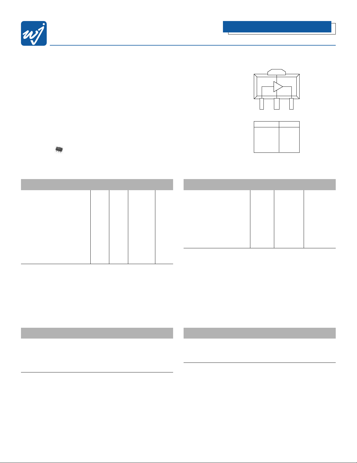
Functional Diagram
High Dynamic Range Amplifier
Absolute Maximum Ratings
Parameter Rating
Operating Case Temperature -40 to +85°C
Storage Temperature -55 to +125 °C
Supply Voltage +6.0 V
Input RF Power (continuous) +10 dBm
Operation of this device above any of these parameters may cause per manent damage.
Ordering Information
Part No. Description
AH1 High Dynamic Range Amplifier
(Available in tape and reel)
AH1-PCB Fully Assembled Application Circuit
The Communications Edge
™
Specifications
Parameter Units Min. Typical Max.
Frequency Range MHz 250-3000
S21 - Gain dB 12.4 13.5
S11 - Input Return Loss
3
dB -8
S22 - Output Return Loss dB -15
Output IP3
2
dBm +37 +41
Output P1dB dBm +21
Noise Figure dB 2.7
Operating Current Range mA 120 150 180
Supply Voltage V 5
Test conditions unless otherwise noted.
1.T = 25°C, Vdd = 5.0, Freq = 800 MHz, 50 ohm system.
2. OIP3 measured with two tones at an output power of 5 dBm/tone separated by 10 MHz.The
suppression on the largest IM3 product is used to calculate the OIP3 using a 2:1 slope rule.
3. S21 and S11 can be improved in the band of interest using a single input shunt microstrip to
ground.
4. Degradation of OIP3 occurs at low temperatures. Minimum typical OIP3 at -40˚C is +35dBm.
5. MTBF calculated with channel temperature at 155˚C.
Typical Parameters
Parameter Units Typical
Frequency MHz 900 1900
S21 dB 14.3 12.6
S11 dB -16.5 -14.5
S22 dB -13.9 -11.7
Output IP3 dBm +41.0 +41.0
Output P1dB dBm +21.2 +21.0
Noise Figure dB 2.5 2.5
Typical parameters reflect performance in an application circuit.
Actual Size
4
123
Function Pin No.
Input 1
Ground 2
Output Bias 3
Ground 4
Page 2
WJ Communications, Inc. • Phone: 1-800-WJ1-4401 • FAX:408-577-6620 • e-mail: sales@wj.com • Web site: www.wj.com February 2002
AH1
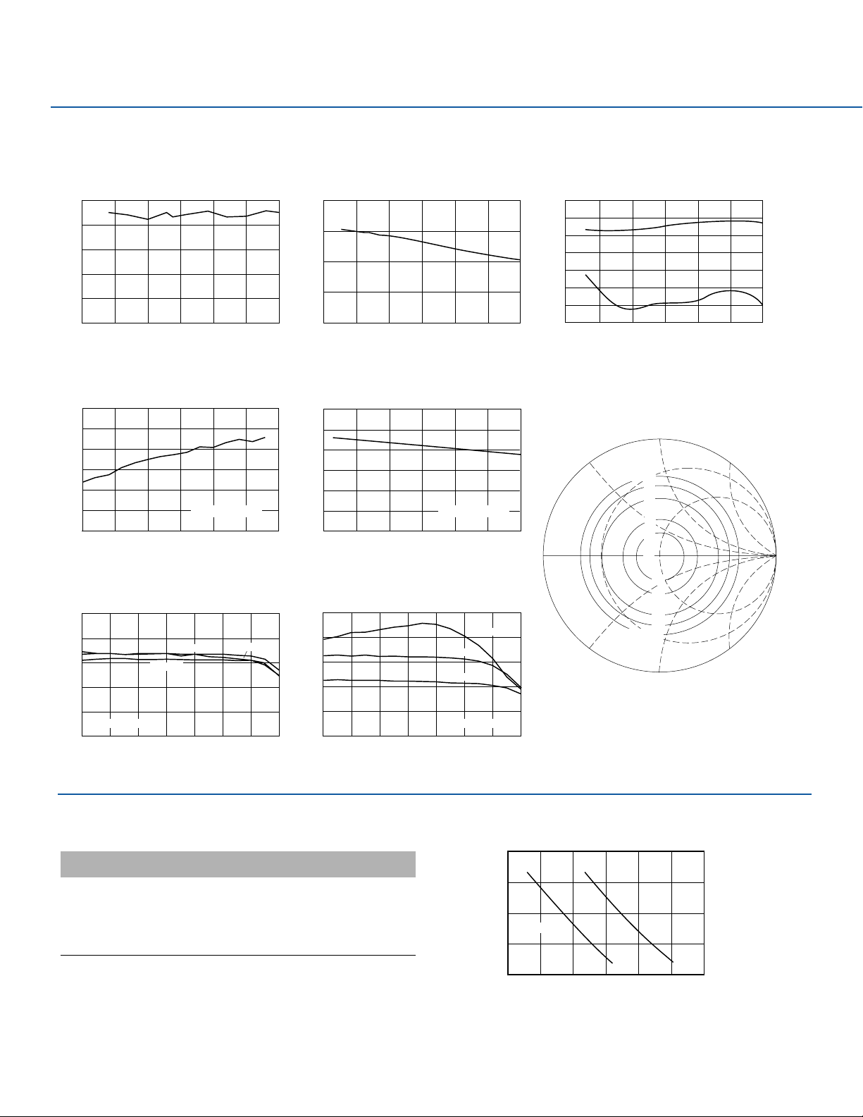
Performance Charts (Vds = 5.0 V, Ids = 150 mA, T = 22°C, unmatched device in a 50 ohm system)
Thermal Specifications
Parameter Rating
Operating Case Temperature -40 to +85°C
Thermal Resistance (Maximum) 59°C/W
Junction Temperature +155°C
(Recommended Maximum)
Notes:
1.Thermal Resistance determined at Maximum Tab Temperature and Maximum Power
Dissipation.
2. Recommended Maximum Junction Temperature insures a MTBF of 1 million hours.
3. Refer to WJ Application Note “AH1 Temperature Effects on Reliability” for more information.
OIP3 vs. Frequency
45
40
35
30
OIP3 (dBm)
25
20
500 1000 1500 2000 2500 35003000
Frequency (MHz)
OIP3 vs. Temperature
43
42
41
40
OIP3 (dBm)
39
38
37
-50 -25 0 25 50 10075
Frequency = 800MHz Frequency = 800MHz
Temperature (C)
Gain vs. Power Out
14.5
14.0
13.5
Gain (dB)
13.0
12.5
12.0
2.5 4.5 6.5 8.5 12.510.5 14.5 16.5
75% Idss
100% Idss
Output Power (dBm) Output Power (dBm)
50% Idss
Gain vs. Frequency* Input/Output Return Loss*
20
15
10
Gain (dB)
5
0
0 500 1000 1500 2000 2500 3000
* without matching circuit * without matching circuit
Frequency (MHz)
0
-5
-10
-15
dB
-20
-25
-30
-35
0 500 1000 1500 25002000 3000
Gain vs. Temperature
15.0
14.5
14.0
13.5
Gain (dB)
13.0
12.5
12.0
-40 -20 0 20 40 60 80
Temperature (C)
OIP3 Lead Pull Circles
Output IP3 vs. Power Out
45
40
35
30
Output IP3 (dBm)
25
20
2.5 4.5 6.5 8.5 12.510.5 14.5 16.5
100% Idss
75% Idss
50% Idss
Frequency = 900 MHzFrequency = 900 MHz
S11
S22
Frequency (MHz)
IP3 = 35
36
37
38
39
41
1.5
2.0
3.0
4.0
VSWR = 5.0
Frequency = 900 MHz
Vds = 5.0 V, 100% Idss, T = 22°C
10
MTBF vs. Temperature
9
8
10
7
10
MTBF (hours)
Ground Tab
6
10
5
10
50 75 100 125 150 175 200
Temperature (°C)
Junction
Page 3

WJ Communications, Inc. • Phone: 1-800-WJ1-4401 • FAX:408-577-6620 • e-mail: sales@wj.com • Web site: www.wj.com February 2002
Application Circuit: 250-650 MHz
Application Circuit: 0.9-2.5 GHz
Typical Performance
Frequency 0.9 GHz 1.9 GHZ 2.4 GHZ
Magnitude S21 14.2 dB 12.4 dB 11.7 dB
Magnitude S11 -18.5 dB -12.9 dB -13.6 dB
Magnitude S22 -14.7 dB -12.6 dB -11.0 dB
OIP3 39.0 dBm 41.0 dBm 40 dBm
Noise Figure 2.7 dB 3.4 dB 3.7 dB
Bias Vd = 5 V, Id = 170 mA
S-Parameters
20
10
0
-10
-20
-30
0 0.5 1 1.5 2 32.5
S11
S21
S22
Frequency (GHz)
Schematic
RF IN
C = 56 pF
300 mil
Z = 22 ohm
L = 5.6 nH
FR4 Board Layout (T = 14 Mil)
0603 Package
C = 56 pF
300 mil
0603 Package
L = 5.6 nH
INPUT OUTPUT
AH1
3 or more Via
Grounds req.
GND
L = 12 nH
C = 56 pF
GND
0603 Package
L = 12 nH
+5 V
C = 56 pF
0603 Package
0603 Package
RF OUT
DC 5 V
C = 56 pF
C = 56 pF
Typical Specifications
Frequency 250 MHz 650 MHZ
Magnitude S21 15.4 dB 14.2 dB
Magnitude S11 -11.0 dB -11.5 dB
Magnitude S22 -19.9 dB -14.0 dB
OIP3 40.0 dBm 40.0 dBm
Noise Figure 2.8 dB 2.8 dB
Bias Vd = 5 V, Id = 160 mA
S-Parameters
20
10
0
-10
Magnitude (dB)
-20
-30
0 100 200 300 400 500 700 800600 1000900
S11
Frequency (MHz)
S21
S22
Schematic
100 mil
RF IN
L = 15 nH
Z = 50 ohm
FR4 Board Layout (T = 14 Mil)
100 mil 200 mil
GATE DRAIN
L = 15 nH
0603 Package
AH1
SOURCE
200 mil
Z = 50 ohm
L = 82 nH
C = 56 pF
0603 Package
L = 82 nH
+5 V
C = 56 pF
0603 Package
C = 56 pF
0603 Package
C = 56 pF
RF OUT
DC 5 V
Page 4

WJ Communications, Inc. • Phone: 1-800-WJ1-4401 • FAX:408-577-6620 • e-mail: sales@wj.com • Web site: www.wj.com February 2002
AH1
Application Circuit: 1900 MHz
Application Circuit: 900 MHz
Typical Specifications
Frequency 900 MHz
Magnitude S21 14.3 dB
Magnitude S11 -16.5 dB
Magnitude S22 -13.9 dB
OIP3 41.0 dBm
Noise Figure 2.5 dB
Bias Vd = 5 V, Id = 170 mA
S-Parameters
20
10
0
-10
Magnitude (dB)
-20
-30
0 0.5 1.0 1.5 2.0 3.02.5
S21
S11
S22
Frequency (GHz)
Schematic
100 mil
RF IN
L = 12 nH
Z = 38 ohm
FR4 Board Layout (T = 14 Mil)
100 mil 200 mil
GATE DRAIN
0603 Package
L = 12 nH
AH1
SOURCE
200 mil
Z = 38 ohm
L = 47 nH
C = 56 pF
0603 Package
L = 47 nH
+5 V
C = 56 pF
0603 Package
C = 56 pF
0603 Package
C = 56 pF
RF OUT
DC 5 V
Typical Specifications
Frequency 1900 MHz
Magnitude S21 12.6 dB
Magnitude S11 -14.5 dB
Magnitude S22 -11.7 dB
OIP3 41.0 dBm
Noise Figure 2.5 dB
Bias Vds = 5 V, Id = 170 mA
S-Parameters
20
10
0
-10
Magnitude (dB)
-20
-30
0 0.5 1.0 1.5 2.0 3.02.5
S21
S11
S22
Frequency (GHz)
Schematic
C = 2.2 pF
RF IN
L = 2.7 nH
100 mil
Z = 38 ohm
L = 6.8 nH
FR4 Board Layout (T = 14 Mil)
0603 Package
C = 2.2 pF
0603 Package
L = 2.7 nH
100 mil 200 mil
GATE DRAIN
0603 Package
L = 6.8 nH
AH1
SOURCE
200 mil
Z = 38 ohm
0603 Package
L = 47 nH
+5 V
L = 47 nH
C = 56 pF
C = 56 pF
0603 Package
C = 56 pF
0603 Package
C = 56 pF
RF OUT
DC 5 V
Page 5

WJ Communications, Inc. • Phone: 1-800-WJ1-4401 • FAX:408-577-6620 • e-mail: sales@wj.com • Web site: www.wj.com February 2002
AH1
Outline Drawing
Specifications and information are subject to change without notice.
Caution! ESD sensitive device.
Land Pattern
Mounting Configuration
Page 6

WJ Communications, Inc. • Phone: 1-800-WJ1-4401 • FAX:408-577-6620 • e-mail: sales@wj.com • Web site: www.wj.com February 2002
AH1
T ypical Test Data
S-Parameters (Vds = +5 V, Ids= 150 mA,T = 22°C, unmatchd device in a 50 ohm system)
Freq (MHz) S11 (Mag) S11 (Ang) S21 (Mag) S21 (Ang) S12 (Mag) S12 (Ang) S22 (Mag) S22 (Ang) K Value
300 0.385 -46.990 5.742 157.037 0.087 3.964 0.089 -66.530 1.062
400 0.374 -53.376 5.633 152.400 0.087 -0.428 0.070 -70.095 1.090
500 0.373 -60.650 5.564 147.518 0.088 -3.847 0.055 -69.277 1.103
600 0.373 -68.718 5.488 142.410 0.088 -6.806 0.043 -75.238 1.116
700 0.376 -76.746 5.409 137.282 0.088 -9.585 0.036 -80.347 1.128
800 0.380 -84.449 5.313 132.011 0.088 -12.184 0.031 -88.416 1.139
900 0.383 -92.673 5.199 126.442 0.087 -14.643 0.028 -102.961 1.154
1000 0.388 -101.021 5.141 121.353 0.087 -17.006 0.029 -115.173 1.159
1100 0.394 -109.189 5.052 116.267 0.087 -19.432 0.029 -127.412 1.168
1200 0.403 -116.975 4.952 111.154 0.087 -21.689 0.031 -124.686 1.176
1300 0.413 -124.433 4.841 106.042 0.086 -24.093 0.033 -90.875 1.185
1400 0.425 -131.566 4.724 101.024 0.086 -26.335 0.035 -93.847 1.198
1500 0.438 -138.169 4.609 96.109 0.085 -28.545 0.034 -94.192 1.210
1600 0.450 -144.356 4.490 91.324 0.084 -30.630 0.035 -91.925 1.224
1700 0.463 -149.987 4.371 86.560 0.084 -32.708 0.035 -138.791 1.241
1800 0.477 -155.154 4.254 81.996 0.083 -34.679 0.035 -131.588 1.253
1900 0.489 -160.003 4.139 77.549 0.082 -36.681 0.036 -120.952 1.272
2000 0.500 -164.309 4.030 73.226 0.081 -38.358 0.039 -112.026 1.289
2100 0.509 -168.120 3.929 69.032 0.081 -40.127 0.042 -104.837 1.306
2200 0.517 -171.726 3.836 64.905 0.080 -41.728 0.046 -99.684 1.322
2300 0.523 -175.359 3.749 60.845 0.079 -43.332 0.049 -94.737 1.344
2400 0.527 -9.058 3.667 56.754 0.079 -44.949 0.052 -92.048 1.366
2500 0.528 176.218 3.600 52.689 0.078 -46.419 0.053 -90.189 1.389
2600 0.526 173.376 3.537 48.710 0.078 -48.000 0.052 -88.680 1.418
2700 0.523 169.003 3.477 44.647 0.078 -49.738 0.050 -87.931 1.450
2800 0.518 164.088 3.422 40.452 0.077 -51.479 0.048 -88.079 1.486
2900 0.513 158.780 3.366 36.157 0.077 -53.246 0.042 -87.362 1.526
3000 0.510 153.067 3.311 31.816 0.077 -55.207 0.034 -82.552 1.561
 Loading...