

Datasheet AGM6424B-C-YBS-T, AGM6424B-C-YBD-T, AGM6424B-C-GBS-T, AGM6424B-C-GBD-T, AGM6424B-C-BBS-T Datasheet (AZDIS)
...Page 1

COMPLETE LCD SOLUTIONS
Page 1 of 14
SPECIFICATIONS FOR
LIQUID CRYSTAL DISPLAY
PART NUMBER: AGM6424B
DATE: JANUARY 21, 2003
AZ DISPLAYS, INC.
Page 2
1. LCD Module
1.1 Main Data
No. Item Contents Unit
(1) Module size 173.0(W) x 73.0(H) x 7.0(D) mm
(2) Viewing area 156.0 (W) x 60.0 (H) mm
(3) Dot Number 640 x 3 (R.G.B) (W) x 240 (H) dots
(4) Dot Size 0.065(W) x 0.225(H) mm
(5) Dot pitch 0.08(W) x 0.24(H) mm
(6) LCD type Color-STN (Negative type)
-
(7) Contrast ratio (30) -
(8) Duty 1/244 -
(9) Viewing direction 6 o clock -
(10) Operating temperature +0 ~ +50 C
(11) Storage temperature -20 ~ +70 C
(12) Backlight Cold Cathode Fluorescent Lamp (CCFL) x 1 pcs
(13) Power Supply Voltage 3.3V -
(14) Weight (120) g
AGM6424B
Page 2 of 14
Page 3
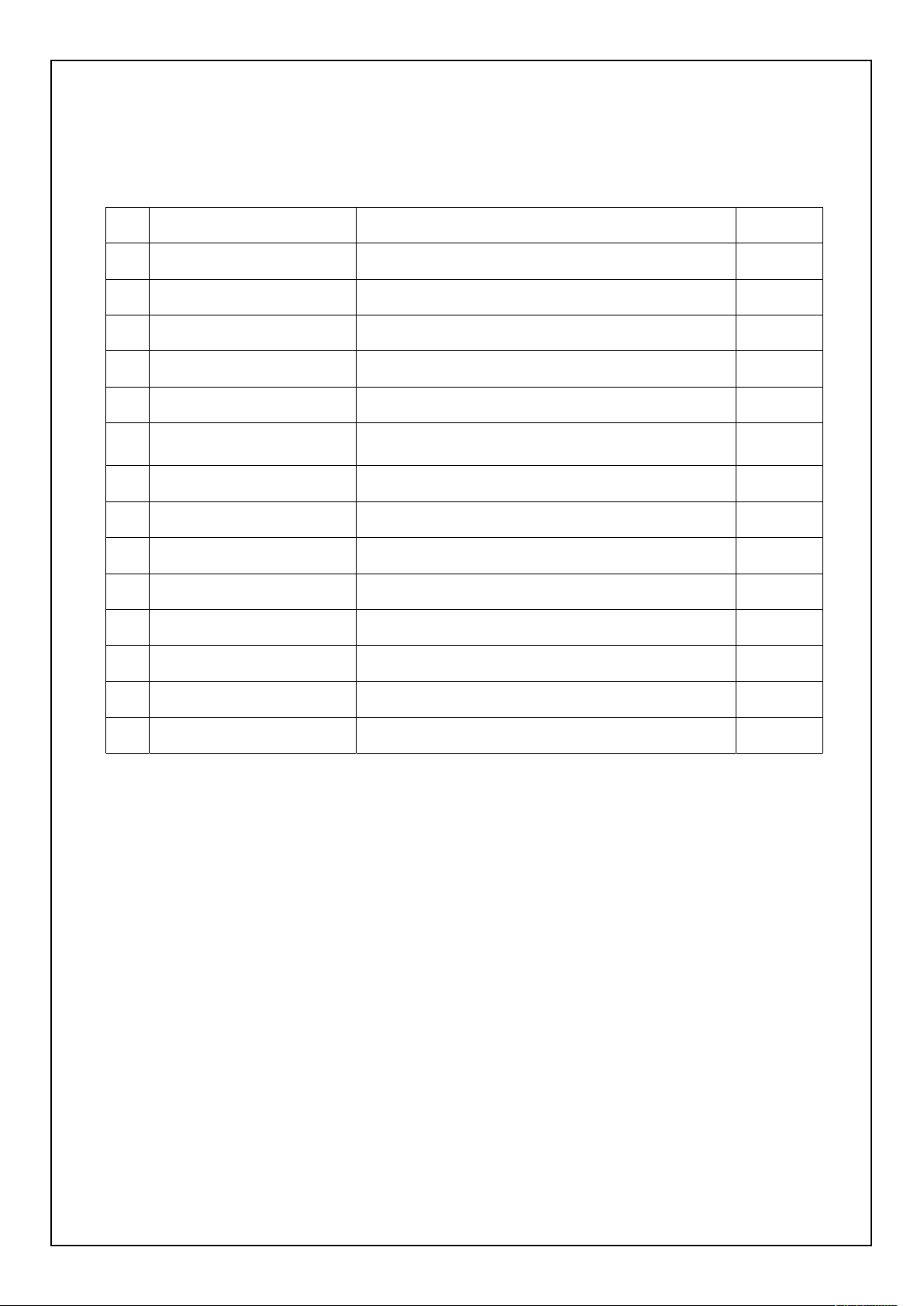
1.2 Interface Pin Connection
CN1 : 52893-2090(MOLEX) / Suitable FPC : Pitch 0.5mm, width 10.5mm
Pin No. Signal Pin Function
1 FLM Scan start-up signal
2
SS
GND
3 CL1 Input data latch signal
4
SS
GND
5 CL2 Data shift clock
6
SS
GND
7 DISP Display control signal H:ON , L:OFF
8
DD
Logic supply voltage
9
CON
Contrast adjust voltage
10
SS
GND
11 D0 Display data
12 D1 Display data
13 D2 Display data
14 D3 Display data
15
SS
GND
16 D4 Display data
17 D5 Display data
18 D6 Display data
19 D7 Display data
20
SS
GND
CN2 : BHSR-02VS-1 (JST) / Suitable
connector : SM02B-BHSS-1-TB (JST)
Pin No. Signal Pin Function
1 H.V Power supply voltage for CFL
2 GND CFL GND
AGM6424B
Page 3 of 14
V
V
V
V
V
V
V
V
Page 4
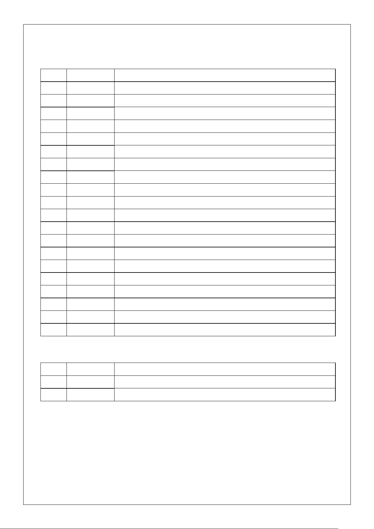
2. Block Diagram
COLOR LCD PANEL
640RGBx240 DOTS
Row Driving Circuit
X1
X240
Column Driving Circuit
Y1
Y1920
Power
Supply
Circuit
VSS
V
DD
DISP
CL2
CL1
GND
H.V
CN2
CN1
CFL
D0~D7
FLM
V
CON
AGM6424B
Page 4 of 14
Page 5
3. Maximum Ratings
3.1 Electrical Absolute Maximum Ratings. (VSS=0V)
Item Symbol Min. Max. Unit
Power supply for Logic VDD-VSS -0.3 7.0 V
Input voltage (Note 1) V
I
-0.3 V
DD
+0.3 V
Note 1. FLM,CL1,CL2,DISP,D0~D7.
Note 2. Ta=25 C
Note 3. Please be sure users are grounded when handling the LCD module.
3.2 Environmental Absolute Maximum Ratings
Storage Operating
Item
MIN. MAX. MIN. MAX.
Remark
Ambient Temperature -20 C 70 C 0 C 50 C Note1,2,3
Humidity Note 4 Note 4 No Condensation
Note 1. Ta at -20 C --------< 48hours, at 70 C --------< 120 hours.
Note 2. Background color changes slightly depending on ambient temperature.
This phenomenon is reversible.
Note 3. When LCM is operated at 0 C, the lifetime of the CFL will be reduced.
The response time at 0 C will increase.
Note 4. Ta<=50 C : 85%RH MAX.
Ta> 50 C : Absolute humidity must be lower than the humidity of 85% RH at 50 C.
AGM6424B
Page 5 of 14
Page 6

4. Electrical Characteristics
4.1 Electrical Characteristics of LCD
Item Symbol Condition MIN. Typ. Max.
Unit
Power Supply for Logic VDD 3.0 3.3 3.6 V
Ta= 5 C (0.8)
Ta=25 C (1.8)
Contrast adjust voltage V
CON
Note(1)
Ta=40 C (2.8)
V
Input Signal Voltage VIH H Level 0.8VDD V
DD
Note (2) VIL L Level 0 0.2VDD
V
Power supply current
Note (3)
I
DD
V
DD
=3.3V (40) mA
Frame Frequency
Note (4)
fFLM (60) (75) (90) Hz
Note (1)
The value is specified as the voltage at which the optimum contrast is obtained.
Note (2) FLM,CL1,CL2,DISP,D0~D7
Note (3) fFLM=75Hz,Ta=25 C,Display pattern is Black/White cross pattern as below.
Note (4) No flicker or ripple phenomenon experienced on the display.
4.2 Electrical Characteristics of Backlight
Item Symbol Min. Typ. Max. Unit Remark
Starting Voltage VS - - (1000) Vrms Ta=5 C
Lamp Voltage VL - (490) - Vrms Ta=25 C
Frequency 40 60 80 KHz Ta=25 C
Lamp Current IL (3.0) (3.5) (4.0) mArms Ta=25 C
Note (1) Starting voltage is higher when the LCM operates at lower temperatures.
Note (2) Average lifetime of CFL will be decreased when LCM is operated at lower
temperatures.
Note (3) CFL lifetime : 10000 hours Min. at I L=3.5mA, Ta=25 C
RGB RGB
AGM6424B
Page 6 of 14
fL
Page 7

5. Optical Characteristics
5.1 Optical Characteristics of LCD
O
Ta= 25 C.(Backlight On)
Item Symbol Condition Min. Typ. Max. Unit Remark
X axis 60 - -
Viewing Angle Range 1, 2 CR 2
Y axis 35 - -
Deg. Note 1,2
Contrast Ratio CR
=0
TBD (30) - -
Note 3,4
Rise tr
=0 , =0
- (340) - ms
Response Time
Fall tf
=0 , =0
- (110) - ms
Note 5
x (0.44) (0.49) (0.54) -
R
y (0.30) (0.35) (0.40) -
x (0.28)
(0.33) (0.38) -
G
y (0.44) (0.49) (0.54) -
x (0.15) (0.20) (0.25) -
B
y (0.16) (0.21) (0.26) -
x (0.27) (0.32) (0.37) -
Color Tone
(CIE Coordinate)
W
y
(0.30) (0.40) -
X
2
X
1
Y( =0 )
Y( =180 )
Eye from ( , 1
)
Eye from (
Note 1. Definition of and Note 2. Definition of Viewing angle 1 and 2
1
CR vs Viewing and
2
1<0 < 2
2.0
CR
AGM6424B
Page 7 of 14
O
>
O
O
O
=0 , =0
O
O
,2)
O
O
O
O
O
O O
O
O
O
O
(0.35)
O
O
O
O
O
O
O
O
O
Page 8

Note 5. Definition of optical response time
Brightness
Non-selected state
Non-selected state
Selected state
10%
90%
tf
tr
CR=
Brightness at selected dot (B1)
Brightness at non-selected dot (B2)
Note 3. Definition of Contrast Ratio CR
B2
B1
Operation voltage
B1
B2
Brightness
Sensor
Back light
Sensor : BM-7
Aperture : 1
Distance : 50 cm
Rise time Fall time
Note 4. Definition of CR and V
OP
CR
V
OP
Operation Voltage
100%
AGM6424B
Page 8 of 14
Page 9

5.2 Optical Characteristics of Backlight
Item Min, Typ. Max. Unit Remark
Brightness - cd/m2 Note 1,2,3
Brightness Uniformity - - +/-30 % Note 2,3,4
Note 1. Measurement Condition:
Display data should be all ON (D0~D7=HIGH).
VDD=3.3V,IL=3.5mArms,V
CON
should be adjusted at the optimum voltage
Note 2. Measured on the following 5 points of the display.
Note 3. The brightness shall be the average of P1~P5 points.
Note 4. Definition of the brightness Uniformity
Max brightness or Min brightness Average brightness
Average brightness
x100%
AGM6424B
Page 9 of 14
(150) -
Y=360 Y=960 Y=1560
X=60
X=120
X=180
Active area
P2 P1
P3
P5 P4
DOTS
DOTS
Page 10

6. Interface Timing Chart
6.1 Timing Chart
(240+n)xT
CL1
X239 X240
Invalid data
X1
X2
R0 B2 G5
B634 G637
G0 R3 B5
R635 B637
B0 G3 R6
G635 R638
R1 B3 G6 B635 G638
G1 R4 B6
R636 B638
B1 G4 R7
G636 R639
R2 B4 G7
B636 G639
G2 R5 B7
R637 B639
X2
X1
FLM
D0~D7
CL1
CL2
D7
D6
D5
D4
D3
D2
D1
D0
T
AGM6424B
Page 10 of 14
Page 11

6.2. Electrical Characteristics
(V
DD
=3.0~4.5V ,V
LCD
= +10.0~ +42.0V, Ta= 0 C~40 C)
Item Symbol Min. Typ. Max. Unit
Shift clock period t
WCK
66 - - ns
Shift clock H pulse wide t
WCKH
23 - - ns
Shift clock L pulse wide t
WCKL
23 - - ns
Data setup time t
DS
10
- - ns
Data hold time t
DH
25
- - ns
Latch pulse H pulse wide t
WLPH
30 - - ns
Shift clock rise to latch pulse rise time tLD 10 - - ns
Shift clock fall to latch pulse fall time tSL 30 - - ns
Latch pulse rise to shift clock rise time tLS 30 - - ns
Latch pulse fall to shift clock fall time tLH 30 - - ns
Enable setup time tTS 12 - - ns
Input signal rise time tR - - 50 ns
Input signal fall time tF - - 50 ns
Output delay tD - - 44 ns
FLM setup time tFS 30 - - ns
FLM hold time tFH 50 - - ns
t
LD
t
WLPH
t
LH
VIH
VIL
t
WCKH
VIH
VIL
t
WCK
LAST DATA
t
SL
tF
t
LS
tR
VIH
VIL
Horizontal retrace period
VIH
VIL
t
DS
tDH
t
FS
t
FH
CL1
CL2
D0~D7
CL1
CL2
FLM
1 2 ..
20
t
WCKL
t
DS
t
DH
TOP DATA
AGM6424B
Page 11 of 14
Page 12

6.3 Power Supply and Signal Sequence
Do not apply DC voltage to the LCD panel because this induces an electrochemical
reaction and reduces its lifetime. Please follow the power supply ON/OFF sequence below
to prevent DC driving of the LCD or latch-up of the LSIs.
SYMBOL MIN. MAX. UNIT COMMENT
tDLD - ms
tCH - ms
tLDH - ms
tDOr 100 ns
tDOf 100 ns
tDLCr - ms
tDLCf - ms
tDLCs - ms
tVH - ms
tDOr
tLDH
0.2x VDD
0.8x VDD
tDLCs
tCH
tDLCr
tDLD
0.8x VDD
tVH
tLDH
tDOf
tDLCs
0.2x VDD
0.8x VDD
tCH
tDLD
tDLCf
0.8x VDD
DISPOFF
CL1
V
DD
POWER ON
POWER OFF
Note 1. Follow the timing sequence as shown above, since an improper sequence may
cause permanent damage to the LCD panel.
V
LCD
Note 2. Please use the DISPOFF function to turn the display off.
AGM6424B
Page 12 of 14
200
0
20
-
-
0
0
20
200
Page 13

6.4 Input Data Allocation Table
Data Signal
D 7 D 6 D 5 D 4 D 3 D 2 D 1 D 0 D 7 D 6 D 5 D
4
D 4 D 3 D 2 D 1 D
0
Y
X
1 2 3 4 5 6 7 8 9 10 11 12 -------
1
9
1
6
1
9
1
7
1
9
1
8
1
9
1
9
1
9
2
0
1 R G B R G B R G B R G B G B R G B
2 R G B R G B R G B R G B G B R G B
3 R G B R G B R G B R G B G B R G B
4 R G B R G B R G B R G B G B R G B
5 R G B R G B R G B R G B G B R G B
6 R G B R G B R G B R G B G B R G B
7 R G B R G B R G B R G B G B R G B
8 R G B R G B R G B R G B G B R G B
9 R G B R G B R G B R G B G B R G B
10 R G B R G B R G B R G B G B R G B
|
|
|
|
|
|
|
|
|
|
|
|
|
|
|
|
|
|
|
|
|
|
|
|
|
|
|
|
|
|
|
|
|
|
|
|
|
|
|
|
|
|
|
|
|
|
|
|
|
|
|
|
|
|
238 R G B R G B R G B R G B G B R G B
239 R G B R G B R G B R G B G B R G B
240 R G B R G B R G B R G B G B R G B
R : RED
G : GREEN
B : BLUE
6.5 Power supply for LCM
VSS
C2
+3.3V
VSS
VDD
-
+
+3.3V
VR
R2
C1
+
R1
Vcon
VCFL
CFL
LCM
AGM6424B
Page 13 of 14
Page 14

CN1 : 52893-2090(MOLEX)
CN2 : BHSR-02VS-1 (JST)
Note 1 : All dimensional tolerance unless otherwise specified+/-0.5
Note 2 : Scale : NTS , Unit : mm
157.6 +/- 0.3
(156.0)
173.0
153.585 +/- 0.1
Active Area Center
Bezel Opening Area
Active Area
(91.1)
73.0
2.7
(39.5)
12.3
CN1
(4.8)
8.7
Inserting
Direction
(20.05)
20
1
0.065
0.08
RGB
0.225
0.24
7.0
Dirrction
Viewing
61.6 +/- 0.3
(60.0)
57.585 +/- 0.1
(105.0)
3.1
CN2
 Loading...