

Datasheet AGM1264F-RLYW-T, AGM1264F-RLYS-T, AGM1264F-RLYH-T, AGM1264F-RLYD-T, AGM1264F-RLGW-T Datasheet (AZDIS)
...Page 1

AZ DISPLAYS, INC.
COMPLETE LCD SOLUTIONS
SPECIFICATIONS FOR
LIQUID CRYSTAL DISPLAY
PART NUMBER: AGM 1264F SERIES
REVISED: December 10, 2001
Page 1 of 11
Page 2
AGM1264F SERIES GRAPHIC MODULE
AZ DISPLAYS, INC.
1.0 MECHANICAL SPECS
2. Overall Module Size 93.0mm(W) x 70.0mm(H) x max 14.0mm(D) for LED backlight
version
93.0mm(W) x 70.0mm(H) x max 9.5mm(D) for reflective
version
3. Dot Size 0.48mm(W) x 0.48mm(H)
4. Dot Pitch 0.52mm(W) x 0.52mm(H)
5. Duty 1/64
6. Controller IC KS0108B
7. LC Fluid Options STN, FSTN
8. Polarizer Options Reflective, Transflective, Transmissive
9. Backlight Options LED
10. Temperature Range Options Standard (0 C ~ 50 C), Wide (-20 C ~ 70 C)
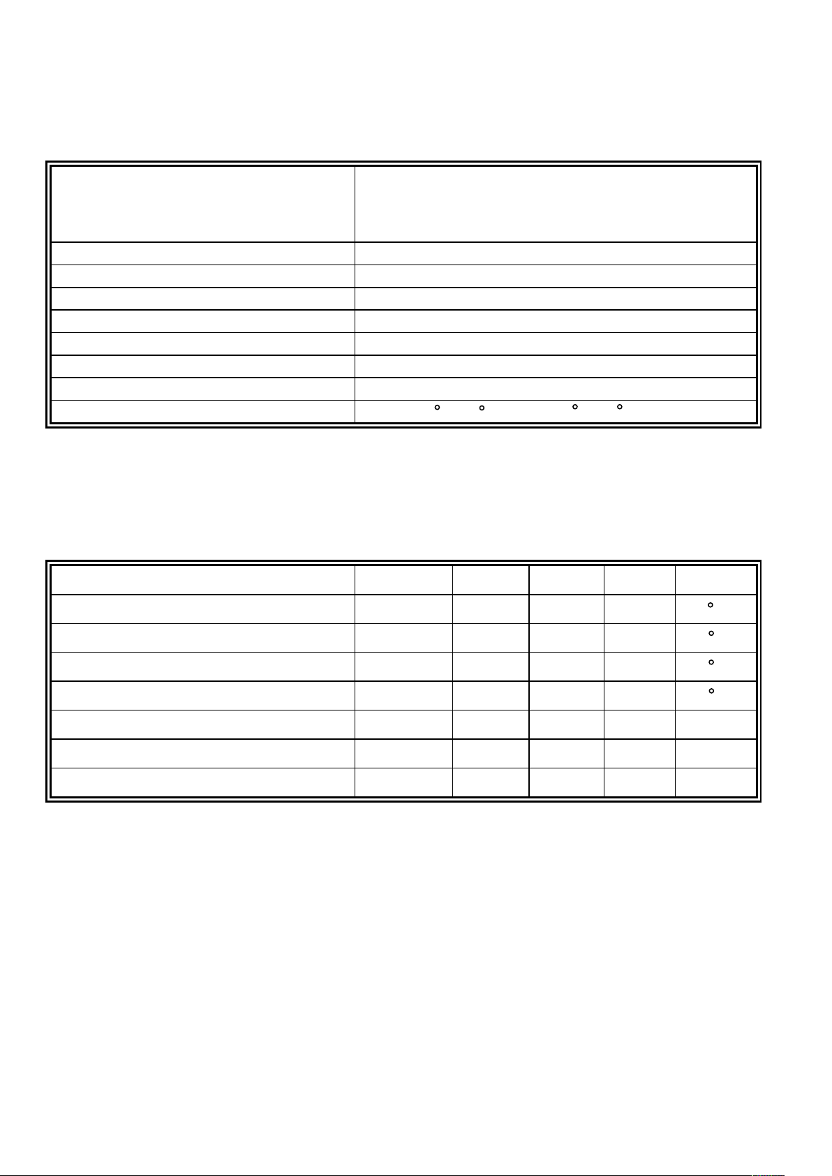
2.0 ABSOLUTE MAXIMUM RATINGS
Item Symbol Min Typ Max Unit
Operating temperature (Standard) Top 0 - 50 C
Storage temperature (Standard) Tst -20 - 70 C
Operating temperature (Wide temperature) Top -20 - 70
C
Storage temperature (Wide temperature) Tst -30 - 80
C
Input voltage Vin Vss Vdd V
Supply voltage for logic Vdd- Vss -0.3 - 7.0 V
Supply voltage for LCD drive Vdd- Vo 9.5 11.5 14.0 V
Page 2 of 11
Page 3
AGM1264F SERIES GRAPHIC MODULE
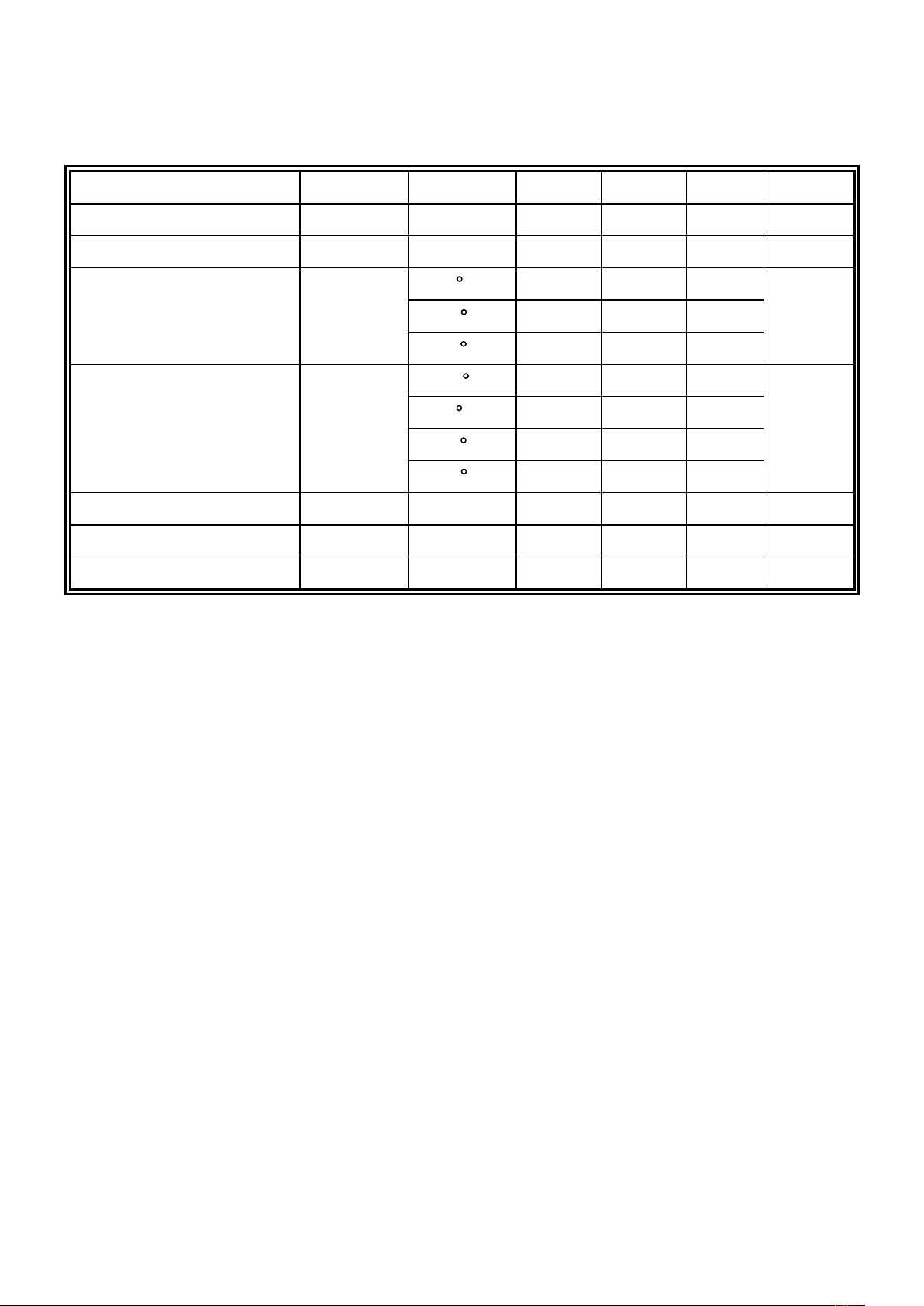
3.0 ELECTRICAL CHARACTERISTICS
Item Symbol Condition Min Typ Max Unit
Input voltage (high) Vih H level 3.5 - Vdd V
Input voltage (low) Vil L level 0 - 1.5 V
0 C - 12.2 12.8
25 C - 11.5 -
Recommended LC Driving
Voltage (Standard Temp)
Vdd - Vo
50 C 10.2 10.6 -
V
-20 C - 13.0 14.0
0 C - 12.2 -
50 C 10.2 10.6 -
Recommended LC Driving
Voltage (Wide Temp)
Vdd -Vo
70 C 9.5 10.0 -
V
Power Supply Current Idd Vdd=5.0V - - 15.0 mA
LED Power Supply Voltage Vfled R=6.8Ω - 4.6 5.0 V
LED Power Supply Current Ifled R=6.8Ω - 470 560 mA
Page 3 of 11
AZ DISPLAYS, INC.
Page 4
AGM1264F SERIES GRAPHIC MODULE
AZ DISPLAYS, INC.
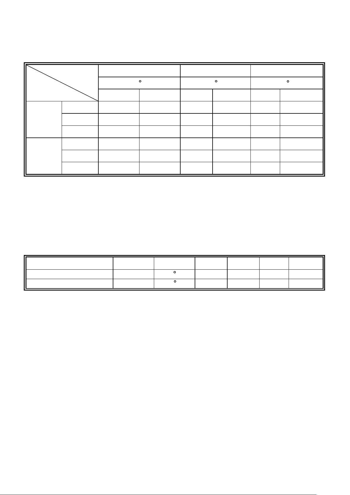
4.0 OPTICAL CHARACTERISTICS
Cr (Contrast Ratio) θ (Viewing Angle) φ (Viewing Angle)
25 C 25 C 25 C
Item
Mode
MIN. TYP. MIN TYP. MIN TYP.
A 2.8 3.05 80 85 - 35
B 7.10 7.70 80 85 - 35
R
C------
A 2.49 2.99 80 85 - 35
B 7.05 7.55 80 85 - 35
S
C------
Note:
R: Reflective
S: Transflective
A: STN Gray
B: STN Yellow
C: FSTN
At: φ=0°, θ=0°
Item Symbol Condition Min Typ Max Unit
Response time (rise) Tr 25
C
- 140 280 ms
Response time (fall) Tf 25 C - 80 160 ms
Page 4 of 11
Page 5

AGM1264F SERIES GRAPHIC MODULE
AZ DISPLAYS, INC.
5.0 BLOCK DIAGRAM
*(optional)
DC to DC
Converter
1. Vss
2. Vdd
3. Vo
4. D/I
5. R/W
6. E
7. DB0
14. DB7
15. CS1
16. CS2
17. RES
18. Vee
LED BACKLIGHT
19. K (-)
20. A (+)
U1
U2
U3
KS0107B
128 X 64
KS0108B
KS0108B
S1 - - - - - - S64 S65 - - - - - - S128
COM1
-
COM64
Page 5 of 11
Page 6

AGM1264F SERIES GRAPHIC MODULE
6.0 PIN ASSIGNMENT
Pin No. Symbol Function Level
1 Vss Ground -
2 Vdd +5V -
3 Vo LCD contrast adjust -
4D/I
H: Data input
L: Instruction code input
H/L
5 R/W H: Data read
L: Data write
H/L
6 E Enable signal
7 DB0 Data bit 0 H/L
8 DB1 Data bit 1 H/L
9 DB2 Data bit 2 H/L
10 DB3 Data bit 3 H/L
11 DB4 Data bit 4 H/L
12 DB5 Data bit 5 H/L
13 DB6 Data bit 6 H/L
14
DB7 Data bit 7 H/L
15
CS1 Chip selection for IC1 H
16
CS2 Chip selection for IC2 H
17
RST
Reset L
18
Vee Power supply for LCD driving -
19
BL- Power Supply for BL- -
20
BL+ Power Supply for BL+ -
7.0 POWER SUPPLY
VR=10K~20K
H/L
Vdd
Vo
Vss
Vee
LCM
+5V
VR
Page 6 of 11
AZ DISPLAYS, INC.
-10V
Page 7

AGM1264F SERIES GRAPHIC MODULE
AZ DISPLAYS, INC.
8.0 TIMING CHARACTERISTICS
Item Symbol Test Condition Min. Typ. Max. Unit
Enable cycle time t
CYC
Fig. a, Fig. b 1000 - - ns
E high level width t
WH
Fig. a, Fig. b 450 - - ns
E low level width t
WL
Fig. a, Fig. b 450 - - ns
Enable rise/fall time Tr , t
f
Fig. a, Fig. b - - 25 ns
Address set up time t
AS
Fig. a, Fig. b 140 - - ns
Address hold time t
AH
Fig. a, Fig. b 10 - - ns
Data delay time t
DDR
Fig. b - - 320 ns
Data set up time t
DSW
Fig. a 200 - - ns
Data hold time (Write) t
DHW
Fig. a 10 - - ns
Data hold time (Read) t
DHR
Fig. b 20 - - ns
DB0~DB7
2.2V
0.8V
t
cyc
Valid Data
0.8V
2.2V
E
R/W
2.2V
CS1~CS2
D/ I
t
AS
0.8V
0.8V
WLt
2.2V
tr
0.8V
2.2V
2.2V
0.8V
t
0.8V
tWH
t
DSW
2.2V
f
0.8V
DHWt
2.2V
t
AH
2.2V
0.8V
Fig. a Interface timing (data write)
Page 7 of 11
Page 8

AGM1264F SERIES GRAPHIC MODULE
AZ DISPLAYS, INC.
2.2V
0.8V
2.2V
2.2V
Valid Data
D/I
R/W
E
DB0~DB7
2.2V
0.8V
CS1~CS2
2.2V
0.8V
2.2V
0.8V
2.2V
0.8V
2.2V
0.8V
2.2V
0.8V
t
AS
t
WL
tWH
t
AH
tDDR
tDHR
t
cyc
t
f
t
r
Fig. b Interface timing (data read)
9.0 RELIABILITY TEST
Evaluations and Assessment*
Storage Condition Content
Current
Consumption
Contrast
Other
Appearances
Operation at high
temperature and
humidity
40 C,90%
RH,240hrs
Twice initial
value or less
More than 80% of
initial value
No abnormality
High temperature
storage
60 C,
240hrs
Twice initial
value or less
More than 80% of
initial value
No abnormality
Low temperature
storage
-20 C,
240hrs
Twice initial
value or less
More than 80% of
initial value
No abnormality
*Evaluations and assessment to be made two hours after returning to room temperature (25 C–5 C).
*The LCDs subjected to the test must not have dew condensation.
Page 8 of 11
Page 9

AZ DISPLAYS, INC.
Part No: AGM1264F
AGM1264F SERIES GRAPHIC MODULE
10.0 MECHANICAL DIAGRAM
Page 9 of 11
Page 10

AGM1264F SERIES GRAPHIC MODULE
AZ DISPLAYS, INC.
11.0 RELATION BETWEEN DISPLAY PATTERN AND DRIVERS
Page 10 of 11
Page 11

AGM1264F SERIES GRAPHIC MODULE
AZ DISPLAYS, INC.
12.0 DISPLAY CONTROL INSTRUCTION
The display control instructions control the internal state of the KS0108B. Instructions are received from
MPU to KS0108B for the display control.
INSTRUCTION D/I R/W DB7 DB6 DB5 DB4 DB3 DB2 DB1 DB0 DESCRIPTION
Display
ON/OFF
000011111 1
Controls the display on or off.
Display RAM data and internal
status is not affected.
0: OFF. 1:ON
Set Address 0 0 0 1 Y address (0~63)
Sets the Y address at the Y
address counter.
Set Page
(X address)
0 0 1 0 1 1 1 Page (0~7)
Sets the X address at the X
address register.
Display Start
Line
0 0 1 1 Display start line (0~63)
Indicates the display data RAM
displayed at the top of the
screen.
Status Read 0 1
BUSY
0
ON/OFF
RESET
0000
Read status:
BUSY 0:Ready
1:In operation
ON/OFF 0:Display ON
1:Display OFF
RESET 0:Normal
1:Reset
Write Display
Data
1 0 Write Data
Writes data DB0~DB7 into
display data RAM. After writing
instruction, Y address is
increased by 1 automatically.
Read Display
Data
1 1 Read Data
Reads data DB0~DB7 from
display data RAM to the data bus.
Page 11 of 11
 Loading...