

Page 1
CALL WAITING DECODER
I. GENERAL DESCRIPTION
This is a new version of Call Waiting service decoder on the telephone. Call Waiting service works by alerting
a customer engaged in a telephone call to a new incoming call. This way the customer can still receive important
calls while engaged in a current call. The Call Waiting decoder can detect dual tone (2130Hz and 2750Hz) alert
signal and generate a valid signal on the data pins for micro controller.
II. FEATURES
• Compatible with Bellcore special report SR-TSV-002476
• 3.6V ~ 6.0V supply voltage
• Call-Waiting (2130Hz plus 2750Hz) Alert Signal Detector
• Good talkdown and talkoff performance
• Sensitivity compensated by adjusting input OP gain
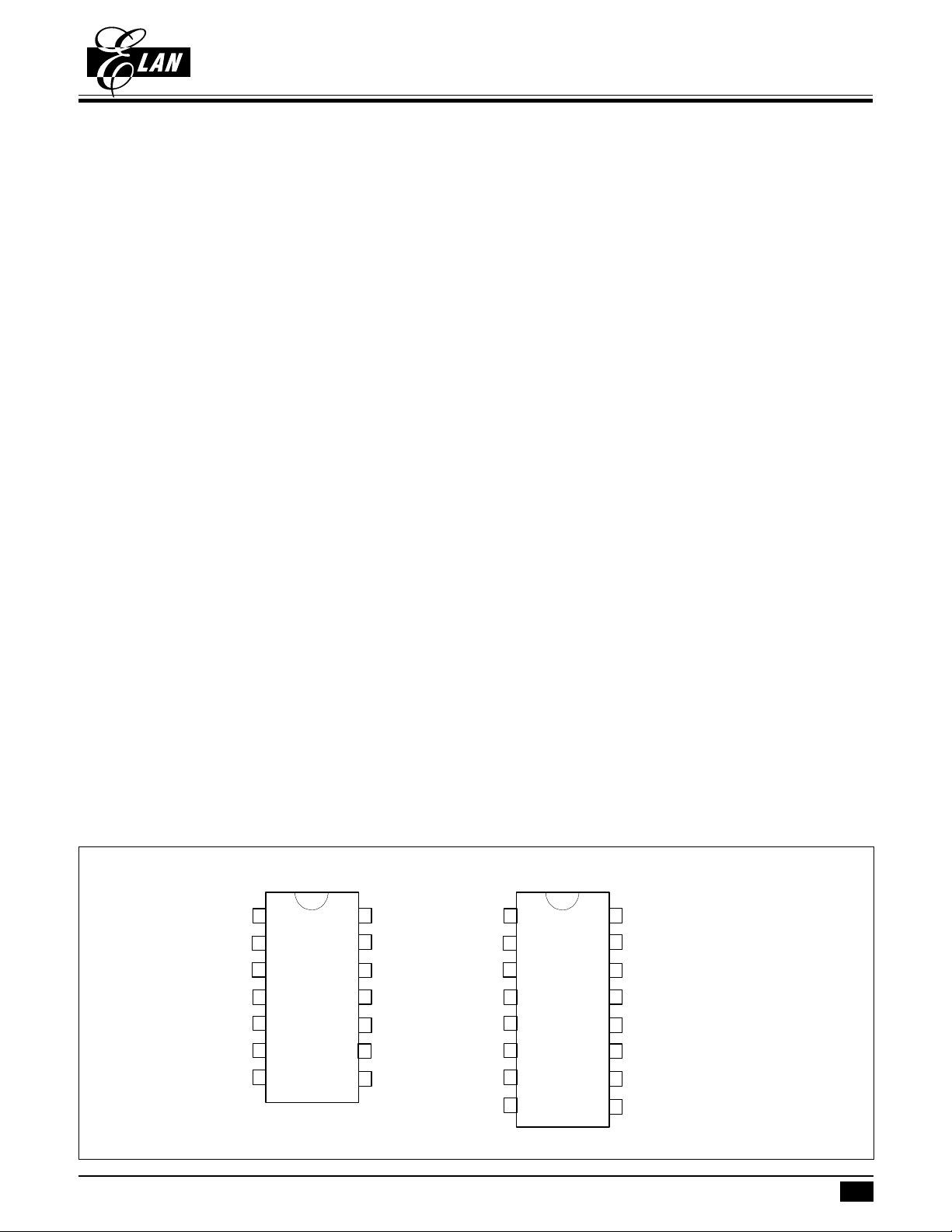
• Package series --- 14-pin DIP or 16-pin SOP (150 mil)
AG8889AP for 14-pin DIP
AG8889N for 16-pin SOP (150 mil)
AG8889
III. APPLICATION
• Feature phones
• Cordless phones
• Adjunct unit (stand alone)
IV. PIN CONFIGURATION
AG8889AP
TIP
RING
OPO
VREF
PWD
VSS
1
2
3
4
NC
5
6
78
14
13
12
11
10
AG8889N
VDD
DO
NC
NC
NC
OSCI
9
OSCO
TIP
RING
OPO
VREF
NC
PWD
VSS
VDD
1
2
3
4
5
6
710
16
15
14
13
12
11
DO
NC
NC
NC
OSCI
OSCO
* This specification are subject to be changed without notice.
NC
89
NC
8.8.2000
1
Page 2
V. FUNCTIONAL BLOCK DIAGRAM
OPO
AG8889
CALL WAITING DECODER
TIP
RING
VREF
Vdd/2
Voltage
Reference
Tone
Filter
Detection Block
DO
Clock
Generator
PWDOSCI OSCO
VI. PIN DESCRIPTIONS
Pin I/O Description
TIP I Tip in should be connected with twisted pair
RING I Ring in should be connected with twisted pair
OPO O Output of OP Amp
VREF Reference voltage Vref = 1/2 Vdd
PWD I This pin is normal low enabling chip on normal operation and ready to detect CAS
tone signals.
This active high input sets the chip into power down mode and disable oscillator to
save power.
OSCI I 3.58MHz oscillator in
OSCO O 3.58MHz oscillator out
DO O DO : used as output, this pin determines whether DO signal is valid or not. High is
valid. Normal low.
VDD Power
GND Ground
NC Non connected
VII. FUNCTIONAL DESCRIPTIONS
Call Waiting service works by alerting a customer engaged in a telephone call to a new incoming call. This way the
customer can still receive important calls while engaged in a current call. The CALL WAITING DECODER can detect
CAS(Call-W aiting Alerting Signal 2130Hz plus 2750Hz) and generate a valid signal on the data pin.
The call waiting decoder is designed to support the Caller Number Deliver feature, which is offered by regional Bell
Operating Companies. The call waiting decoder has three blocks, including differential amplifier , tone filter detection block
In a typical application, this IC receives Tip and Ring signals from twisted pairs. The signals as inputs of dif ferential
amplifier, and the dif ferential amplifier sends input signal to a band pass tone filter. Once the signal is filtered, the
digital detection block decodes the information. The output data made available at DO pin.
This IC is used for detecting CAS signals. Once the signal is detected, the detection indication is shown on the data
output DO pin. The DO pin is normal low . When this IC detects 2130Hz and 2750Hz frequency at the same time, then
DO pin goes to high.
* This specification are subject to be changed without notice.
8.8.2000
2
Page 3
AG8889
CALL WAITING DECODER
DC CHARACTERISTIC
VDD=5V, Vss=0V, T a=25°C, fOSC=3.58MHz
Sym. Description Condition Min. Typ. Max. Unit
VDD operating supply voltage 3.6 6 V
IDD operating supply current 3.3 5 mA
VIL low level input voltage 1.5 V
VIH high level input voltage 3.5 V
VOL low level output voltage load=1mA 0.4 V
VOH high level output voltage load=1mA 4.6 V
Note: 1.both tones in the composite signal have equal amplitude.
2.tone pair is deviated by 0.5%.
3.addes a 0.1uf capacitor between Power and Ground.
AC ELECTRICAL CHARACTERISTIC
(VDD=+5V,Ta=+25°C)
CHARACTERISTIC Min. Typ. Max. Unit
Input sensitivity TIP and RING pins ,Vdd=+5V, Input G=1 -38 dBm
Input frequency tolerance for 2130Hz ±1.2 %
Input frequency tolerance for 2750Hz ±1.2 %
* This specification are subject to be changed without notice.
8.8.2000
3
Page 4

WAVE FORM TIMING
DO timing:
line event
normal on hook
off hook
engaged call
AG8889
CALL WAITING DECODER
alert
tone
(~80ms)
Tvd
CAS
Tvd=Tfvd+Tdvd
Tfvd
Tdvd
Tinvd
Tfinvd
Tdinvd
Tinvd=Tfinvd+Tdinvd
OSC timing:
power off
Power
on/off
PWD
Tosc
OSCI
(OSCO)
Sym. Description Min. Typ. Max. Unit
Tfvd filter output signal valid delay 6 ms
Tfinvd filter output signal invalid delay 6 ms
Tdvd digital delay of valid signal 36 ms
Tdinvd digital delay of invalid signal 20 ms
Tvd total delay of valid signal 42 ms
Tinvd total delay of invalid signal 26 ms
alert input alert tone length 80 ms
tone (2130 ,2750 Hz @ -20dBm )
Tosc Oscillator enable delay time 10 ms
OSC off
power on
OSC on
Tosc
OSC off
Note: detected alert tone length shown above is assumed that no speech signals input.
test under alert tone signal = -22dBm (600Ω)
* This specification are subject to be changed without notice.
8.8.2000
4
Page 5

CALL WAITING DECODER
APPLICATION CIRCUIT 1
When PWD pin (pin 6) is controlled by MCU or external hook detect circuit, the users can use the following
application. (pin6 is connected to control pin of MCU or hook detect output)
AG8889
TIP
RING
0.01u
250V
0.01u
250V
Note :
KYOCERA
Y1
KBR-3.58MSB202
C1
33p
C2
33p
KBR-3.58MSB202 tolerrance :
-0.10% ~+0.15%
430k
430k
5V
39k
39k
62k
470k
51k
47p
3
OPO
1
TIP
RING
2
4
VREF
7
GND
MCU
VDD
DO
PWD
OSCI
OSCO
8-bit
5V
14
0.1u
13
6
9
8
C1
33p
Y1
3.58MHz
C2
33p
* This specification are subject to be changed without notice.
8.8.2000
5
Page 6

CALL WAITING DECODER
APPLICATION CIRCUIT 2
In some application, the call waiting decoder is always powered on , the PWD pin (pin 6) can not be directly
connected to the ground, the users have to use the following application. (pin6 is connected with a capacitor to
VDD and connected with a resistor to the ground).
AG8889
TIP
RING
0.01u
250V
0.01u
250V
Note :
KYOCERA
Y1
KBR-3.58MSB202
C1
33p
C2
33p
KBR-3.58MSB202 tolerrance :
-0.10% ~+0.15%
430k
430k
5V
39k
39k
62k
470k
51k
3
47p
1
2
4
OPO
TIP
RING
VREF
GN
7
D
8-bit
MCU
VD
D
DO
PWD
OSCI
OSCO
5V
14
0.1u
5V
13
6
9
8
C1
33p
Y1
3.58MHz
C2
33p
470p
20k
* This specification are subject to be changed without notice.
8.8.2000
6
Page 7

APPLICATION NOTE
1. VDD, GND
To reduce noise effects, separate the analog and digital systems close to the device. For both the digital and
analog VDD pins, use a ceramic capacitor of about 0.1uF set as close as possible to the pin to bypass to the
respective GND's.
2. PWD pin
By connecting PWD pin to GND, normal mode is obtained. In the normal mode, the oscillator is activated then
ready to decode CAS signal and the chip consumes operating current. By connecting PWD pin to VDD, the
chip is on power down mode and the chip consumes just stand-by current.
3. OPO pin
This pin is the gain adjustment of internal OP Amp.
4. XIN, XOUT pins
If the resonator is used, two capacitors about 33pF and 1M( resistor have to be connected for frequency
accuracy .
AG8889
CALL WAITING DECODER
* This specification are subject to be changed without notice.
8.8.2000
7
 Loading...