

Page 1
Alpha Industries, Inc. [781] 935-5150 • Fax [617] 824-4579 • Email sales@alphaind.com • www.alphaind.com 1
Specifications subject to change without notice. 12/99A
Ka Band Power GaAs MESFET Chip
Features
■ 21 dBm Output Power @ 18 GHz
■ High Associated Gain, 9 dB @ 18 GHz
■ High Power Added Efficiency, 25%
■ Broadband Operation, DC–40 GHz
■ 0.25 µm Ti/Pd/Au Gates
■ Passivated Surface
■ Through-Substrate Via Hole Grounding
Description
The AFM04P2-000 is a high performance power GaAs
MESFET chip having a gate length of 0.25 µm and a
total gate periphery of 400 µm. The device has
excellent gain and power performance through 40 GHz,
making it suitable for a wide range of commercial and
military applications in oscillator and amplifier circuits. It
employs Ti/Pd/Au gate metallization and surface
passivation to ensure a rugged, reliable part. Throughsubstrate via holes are incorporated into the chip to
facilitate low inductance grounding of the source for
improved high frequency and high gain performance.
AFM04P2-000
Parameter Test Conditions Min. Typ. Max. Unit
Saturated Drain Current (I
DSS
)
VDS= 2 V, VGS= 0 V
90.0 140.0 190.0 mA
Transconductance (gm) 60.0 80.0 mS
Pinch-off Voltage (VP) VDS= 5 V, IDS= 1 mA 1.0 3.0 5.0 -V
Gate to Drain IGD= -400 µA 8.0 12.0 -V
Breakdown Voltage (V
bgd
)
Output Power at 1 dB 21.0 dBm
Compression (P
1 dB
)
Gain at 1 dB Compression (G
1 dB
)
VDS= 5 V, IDS= 70 mA, F = 18 GHz
9.0 dB
Power Added Efficiency (ηadd) 25.0 %
Output Power at 1 dB 20.0 dBm
Compression (P
1 dB
)
Gain at 1 dB Compression (G
1 dB
)
VDS= 5 V, IDS= 70 mA, F = 30 GHz
5.0 dB
Power Added Efficiency (ηadd) 15.0 %
Thermal Resistance (Θ
JC
) T
BASE
= 25°C 250.0 °C/W
Electrical Specifications at 25°C
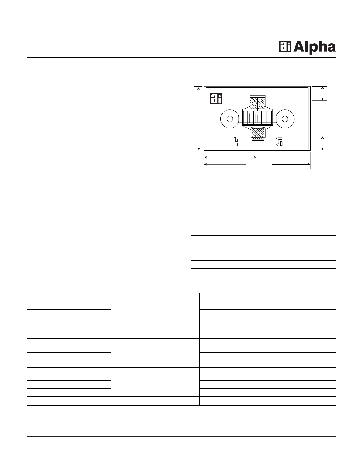
0.395 mm
0.327 mm
Drain
Gate
0.655 mm
0.110 mm
0.110 mm
Characteristic Value
Drain to Source Voltage (VDS) 6 V
Gate to Source Voltage (VGS) -4 V
Drain Current (IDS) I
DSS
Gate Current (IGS) 1 mA
Total Power Dissipation (PT) 700 mW
Storage Temperature (TST) -65 to +150°C
Channel Temperature (TCH) 175°C
Absolute Maximum Ratings
Chip thickness = 0.1 mm.
Page 2
2 Alpha Industries, Inc. [781] 935-5150 • Fax [617] 824-4579 • Email sales@alphaind.com • www.alphaind.com
Specifications subject to change without notice. 12/99A
Ka Band Power GaAs MESFET Chip AFM04P2-000
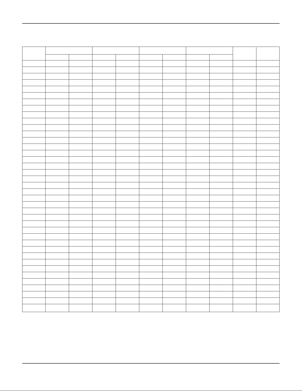
Typical S-Parameters (VDS= 5 V, IDS= 70 mA)
Freq.
S
11
S
21
S
12
S
22
MAG
(GHz) Mag. Ang. Mag. Ang. Mag. Ang. Mag. Ang. k (dB)
2 0.969 -37.191 5.040 153.579 0.029 68.605 0.550 -18.296 0.100 22.364
3 0.958 -54.069 4.740 141.521 0.041 59.064 0.533 -26.529 0.150 20.613
4 0.935 -69.318 4.398 130.518 0.051 50.587 0.514 -33.959 0.200 19.278
5 0.913 -82.889 4.050 120.568 0.058 43.171 0.497 -40.630 0.250 18.247
6 0.893 -94.881 3.719 111.573 0.064 36.722 0.482 -46.663 0.299 17.658
7 0.877 -105.468 3.415 103.398 0.068 31.107 0.471 -52.183 0.349 17.104
8 0.863 -114.843 31.420 95.911 0.071 26.196 0.462 -57.310 0.398 16.464
9 0.852 -123.189 2.898 88.991 0.073 21.873 0.456 -62.138 0.447 15.986
10 0.843 -130.670 2.683 82.540 0.074 18.042 0.453 -66.738 0.496 15.566
11 0.836 -137.422 2.492 67.477 0.075 14.624 0.452 -71.161 0.544 15.193
12 0.831 -143.563 2.322 70.736 0.076 11.558 0.453 -75.442 0.593 14.858
13 0.826 -149.188 2.171 65.267 0.076 8.796 0.455 -79.606 0.641 14.447
14 0.823 -154.374 2.036 60.027 0.076 6.302 0.459 -83.671 0.688 14.285
15 0.821 -159.187 1.914 54.985 0.065 4.047 0.464 -87.648 0.735 14.037
16 0.819 -163.679 1.805 50.114 0.074 2.007 0.470 -91.546 0.781 13.811
17 0.818 -167.895 1.605 45.393 0.074 0.167 0.477 -95.372 0.827 13.063
18 0.817 171.872 1.615 40.805 0.073 -1.486 0.484 -99.129 0.872 13.412
19 0.817 -175.369 1.532 36.335 0.072 -2.961 0.492 -102.821 0.916 13.235
20 0.817 -179.221 1.456 31.973 0.071 -4.266 0.501 -106.451 0.959 13.071
21 0.818 177.359 1.386 27.760 0.060 -5.405 0.510 -110.021 1.001 12.753
22 0.819 174.083 1.321 23.535 0.069 -6.382 0.520 -113.533 1.041 11.534
23 0.820 170.936 1.261 19.445 0.068 -7.201 0.530 -116.989 1.069 10.915
24 0.821 167.905 1.205 15.343 0.067 -7.863 0.540 -120.389 1.116 10.431
25 0.822 164.969 1.512 11.498 0.066 -8.371 0.551 -123.737 1.150 10.024
26 0.824 162.148 1.103 6.633 0.065 -8.728 0.561 -127.031 1.181 9.671
27 0.825 159.403 1.057 3.836 0.064 -8.937 0.572 -130.275 1.210 9.358
28 0.826 156.737 1.013 0.105 0.063 -9.004 0.583 -133.468 1.235 9.080
29 0.829 154.144 0.972 -3.563 0.062 -8.937 0.594 -136.612 1.256 8.830
30 0.831 151.618 0.922 -7.169 0.062 -8.740 0.605 -139.606 1.273 8.604
31 0.833 149.155 0.895 -10.714 0.061 -8.427 0.616 -142.754 1.285 8.403
32 0.835 146.649 0.860 -14.200 0.061 -8.010 0.627 -145.754 1.292 8.222
33 0.836 144.398 0.826 -17.627 0.061 -7.502 0.638 -148.608 1.294 8.061
34 0.838 142.097 0.794 -20.996 0.061 -6.920 0.648 -151.615 1.291 7.920
35 0.840 139.845 0.764 -24.308 0.061 -6.281 0.659 -154.477 1.283 7.797
36 0.842 137.637 0.734 -27.563 0.061 -5.604 0.670 -157.293 1.270 7.694
37 0.844 135.472 0.706 -30.761 0.061 -4.907 0.680 -160.065 1.251 7.611
38 0.846 133.347 0.679 -33.903 0.061 -4.209 0.690 -162.693 1.228 6.550
39 0.848 131.261 0.653 -36.988 0.062 -3.525 0.700 -165.477 1.202 7.513
40 0.850 129.211 0.628 -40.017 0.063 -2.874 0.710 -168.117 1.171 7.504
S-Parameters include the effects of two 0.8 mil diameter bond wires, each 10 mil long, to each of the gate and drain terminals.
Page 3

Parameter Description Unit Default
BETA Transconductance Coefficient A/V
2
0.09464
V
PO
Pinch-off voltage V -1.8760
U Mobility degradation fitting parameter /V 0.3599
GAMA Slope parameter of pinch-off voltage 0.03458
Q Power law parameter 1.6560
NG Subthreshold slope gate parameter 0.6025
ND Subthreshold slope drain parameter 0.6050
DELT Slope of drain characteristics in the saturated region /A, V 0.5633
ALFA Slope of drain characteristics in the linear region /V 1.9400
T Channel transmit-time delay pS 6.4330
C
GSO
Gate-source Schottky barrier capacitance at VGS= 0 pF 0.4232
C
GDO
Gate-drain Schottky barrier capacitance at VGS= 0 pF 0.03138
V
BI
Built-in barrier potential V 1.200
IS Diode saturation current A 0.563e-12
N Diode ideality factor 1.1000
IBO Breakdown saturation current A 1.000e-16
NR Breakdown ideality factor 10.0
V
BD
Breakdown voltage V 20.00
RG Gate terminal resistance Ω 1.0000
RD Drain terminal resistance Ω 2.0000
RS Source terminal resistance Ω 0.8000
LG Gate lead inductance nH 0.5572
LD Drain lead inductance nH 0.2279
LS Source lead inductance nH 0.03532
CDS Drain-source capacitance pF 0.1555
RDSD Channel trapping resistance Ω 107.99
CDSD Low frequency trapping resistance nF 12.03
CGE Gate-source electrode capacitance fF 7.7240
CDE Drain-source electrode capacitance fF 9.4390
Ka Band Power GaAs MESFET Chip AFM04P2-000
Alpha Industries, Inc. [781] 935-5150 • Fax [617] 824-4579 • Email sales@alphaind.com • www.alphaind.com 3
Specifications subject to change without notice. 12/99A
Power Derating
0
0.25
0.50
0.75
1.00
0 50 100 150 200
Total Power Dissipation P
T
(W)
T
BASE
(˚C)
I-V
0
30
60
90
120
150
012
3
54
-0.5 V
-1.0 V
-1.5 V
-2.0 V
-2.5 V
VDS (V)
l
DS
(mA)
VGS = 0 V
Typical Performance Data
TOM-2 Model Parameters
 Loading...