

Page 1
AFE1224
®
2Mbps, Single Pair ANALOG FRONT END
FEATURES
● E1/T1 SINGLE PAIR 2B1Q
● PROGRAMMABLE POWER DISSIPATION
● 28-LEAD SSOP
● 64kbps TO 2320kbps OPERATION
DESCRIPTION
Burr-Brown’s Analog Front End minimizes the size
and cost of a single pair High bit rate Digital Subscriber Line (HDSL) system by providing all of the
active analog circuitry needed to connect an HDSL
digital signal processor to an external compromise
hybrid and an HDSL line transformer. The transmit
and receive filter responses automatically change with
clock frequency, allowing the AFE1224 to operate
over a wide range of data rates. The power dissipation
of the device can be reduced under digital control for
operation at lower speeds. The AFE1224 will operate
at bit rates from 64kbps to 2.320Mbps.
©
1999 Burr-Brown Corporation PDS-1548A Printed in U.S.A. June, 1999
For most current data sheet and other product
information, visit www.burr-brown.com
International Airport Industrial Park • Mailing Address: PO Box 11400, Tucson, AZ 85734 • Street Address: 6730 S. Tucson Blvd., Tucson, AZ 85706 • Tel: (520) 746-1111
Twx: 910-952-1111 • Internet: http://www.burr-brown.com/ • Cable: BBRCORP • Telex: 066-6491 • FAX: (520) 889-1510 • Immediate Product Info: (800) 548-6132
● SCALEABLE DATA RATE
● PIN COMPATIBLE WITH AFE1124
● COMPLETE ANALOG INTERFACE
● –40°C TO +85°C OPERATION
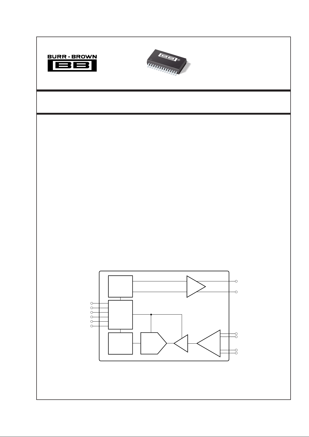
Functionally, this unit consists of a transmit and a
receive section. The transmit section generates analog
signals from 2-bit digital symbol data and filters the
analog signals to create 2B1Q symbols. The on-board
differential line driver provides a 13.5dBm signal to
the telephone line. The receive section filters and
digitizes the symbol data received on the telephone
line. The AFE1224 operates on a single 5V supply.
The digital circuitry in the unit can be connected to a
supply from 3.3V to 5V. The chip uses only 355mW
for full-speed operation. It is housed in a 28-lead
SSOP package.
∆Σ
Modulator
Pulse Former
PGA
Difference
Amplifier
Patents Pending
AFE1224
Line Driver
txLINE
txLINE
rxHYB
rxHYB
rxLINE
rxLINE
tx and rx
Control
Registers
tx and rx
Interface
Lines
Decimation
Filter
AFE1224
Page 2

2
®
AFE1224
SPECIFICATIONS
All specifications at 25°C, AVDD = +5V, DVDD = +3.3V, f
TX
= 1168kHz (E1 rate) and normal power mode, unless otherwise noted.
The information provided herein is believed to be reliable; however, BURR-BROWN assumes no responsibility for inaccuracies or omissions. BURR-BROWN
assumes no responsibility for the use of this information, and all use of such information shall be entirely at the user’s own risk. Prices and specifications are subject
to change without notice. No patent rights or licenses to any of the circuits described herein are implied or granted to any third party. BURR-BROWN does not
authorize or warrant any BURR-BROWN product for use in life support devices and/or systems.
AFE1224E
PARAMETER COMMENTS MIN TYP MAX UNITS
RECEIVE CHANNEL
Number of Inputs Differential 2
Input Voltage Range Balanced Differential
(1)
±3.0 V
Common-Mode Voltage AV
DD
/2 V
Input Impedance, All Inputs
78kbps 32 kΩ
1168kbps 21 kΩ
2320kbps 10 kΩ
Input Capacitance 10 pF
Input Gain Matching Line Input vs Hybrid Input ±2%
Resolution 14 Bits
Programmable Gain 0dB, 3dB, 6dB, 9dB and 12dB 0 +12 dB
Settling Time for Gain Change 6
Symbol Periods
Gain + Offset Error Tested at Each Gain Range 5 %FSR
(2)
Output Data Coding Binary Two’s Complement
Data Rate Normal Power 64 2320 kbps
Medium Power 64 1168 kbps
Low Power 64 320 kbps
Output Word Rate Normal Power
(3)
32 1168 kHz
TRANSMIT CHANNEL
Transmit Clock Rate, f
TX
Symbol Rate, Normal Power 196 1168 kHz
Symbol Rate, Medium Power 96 584 kHz
Symbol Rate, Low Power 80 160 kHz
Transmit –3dB Point 2320kbps 485 kHz
1168kbps 292 kHz
784kbps 196 kHz
Transmit Power
(5)
13 13.5 14 dBm
Pulse Output See Typical Performance Curves
Common-Mode Voltage (V
CM
) AVDD/2 V
Output Resistance DC to 1MHz 1 Ω
TRANSCEIVER PERFORMANCE
Uncancelled Echo
(5)
rxGAIN = 0dB, Loopback Enabled –71 –68.5 dB
rxGAIN = 0dB, Loopback Disabled –71 –68.5 dB
rxGAIN = 3dB, Loopback Disabled –74 –71 dB
rxGAIN = 6dB, Loopback Disabled –76 –73.5 dB
rxGAIN = 9dB, Loopback Disabled –78 –75.5 dB
rxGAIN = 12dB, Loopback Disabled –80 –77.5 dB
DIGITAL INTERFACE
Logic Levels
V
IH
|IIH| < 10µADV
DD
–1 DVDD +0.3 V
V
IL
|IIL| < 10µA –0.3 +0.8 V
V
OH
IOH = –20µADV
DD
–0.5 V
V
OL
IOL = 20µA +0.4 V
t
rx1
Interface 3 4.6 ns
POWER
Analog Power Supply Voltage Specification 5 V
Operating Range 4.75 5.25 V
Digital Power Supply Voltage Specification 3.3 V
Operating Range 3.15 5.25 V
Power Dissipation
(4, 5)
Normal Power 385 mW
Medium Power 300 mW
Low Power 240 mW
Power Dissipation
(4, 5)
Normal Power, DVDD = 5V 415 mW
Power Supply Rejection Ratio 55 dB
TEMPERATURE RANGE
Operating
(6)
–40 +85 °C
NOTES: (1) With a balanced differential signal, the positive input is 180° out-of-phase with the negative input, therefore the actual voltage swing about the commonmode voltage on each pin is ±1.5V to achieve a total input range of ±3.0V or 6Vp-p. (2) FSR is Full-Scale Range. (3) The output data is available at twice the symbol
rate with interpolated values. (4) With a pseudo-random equiprobable sequence of HDSL pulses; 13.5dBm applied to the transformer (16.5dBm output from txLINE+
and txLINE–). (5) See the Discussion of Specifications section of this data sheet for more information. (6) Functionality only guaranteed over temperature range.
Page 3
3
®
AFE1224
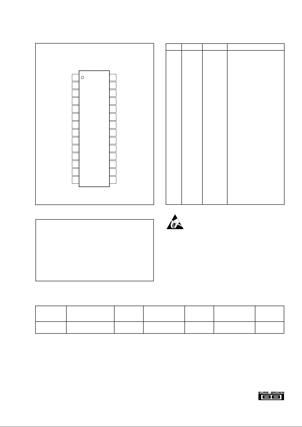
PIN CONFIGURATION
Analog Inputs: Current .............................................. ±100mA, Momentary
±10mA, Continuous
Voltage.................................. AGND –0.3V to AV
DD
+0.3V
Analog Outputs Short Circuit to Ground (+25°C)..................... Continuous
AV
DD
to AGND .........................................................................–0.3V to 6V
DV
DD
to DGND.........................................................................–0.3V to 6V
Digital Input Voltage to DGND .................................. –0.3V to DV
DD
+0.3V
Digital Output Voltage to DGND ...............................–0.3V to DV
DD
+0.3V
AGND, DGND, Differential Voltage .................................................... 0.3V
Junction Temperature (T
J
) ............................................................. +150°C
Storage Temperature Range .......................................... –40°C to +125°C
Lead Temperature (soldering, 3s).................................................. +260°C
Power Dissipation .......................................................................... 700mW
ABSOLUTE MAXIMUM RATINGS
ELECTROSTATIC
DISCHARGE SENSITIVITY
This integrated circuit can be damaged by ESD. Burr-Brown
recommends that all integrated circuits be handled with
appropriate precautions. Failure to observe proper handling
and installation procedures can cause damage.
ESD damage can range from subtle performance degradation
to complete device failure. Precision integrated circuits may
be more susceptible to damage because very small parametric
changes could cause the device not to meet its published
specifications.
PACKAGE SPECIFIED
DRAWING TEMPERATURE PACKAGE ORDERING TRANSPORT
PRODUCT PACKAGE NUMBER
(1)
RANGE MARKING NUMBER
(2)
MEDIA
AFE1224E SSOP-28 324 –40°C to +85°C AFE1224E AFE1224E Rails
"""""AFE1224E/1K Tape and Reel
NOTES: (1) For detailed drawing and dimension table, please see end of data sheet, or Appendix C of Burr-Brown IC Data Book. (2) Models with a slash (/ ) are
available only in Tape and Reel in the quantities indicated (e.g., /1K indicates 1000 devices per reel). Ordering 1000 pieces of “AFE1224E/1K” will get a single 1000piece Tape and Reel. For detailed Tape and Reel mechanical information, refer to Appendix B of Burr-Brown IC Data Book.
PACKAGE/ORDERING INFORMATION
Top View SSOP-28
PIN # TYPE NAME DESCRIPTION
1 — NC No Connection
2 — NC No Connection
3 Power DV
DD
Digital Supply (+3.3 to +5V)
4 Ground DGND Digital Ground
5 Input txbaudCLK Transmit Baud Clock
6 Input tx48xCLK Transmit Clock at 48x Baud Clock
7 Input Data In Input Data Word
8 Input rxbaudCLK Receive Baud Clock
9 Input rx48xCLK Receive Clock at 48x Baud Clock
10 Output Data Out Output Data Word
11 Power DV
DD
Digital Supply (+3.3V to +5V)
12 Ground DGND Digital Ground
13 Power AV
DD
Analog Supply (+5V)
14 Input rxHYB–
Negative Input from Hybrid Network
15 Input rxHYB+ Positive Input from Hybrid Network
16 Input rxLINE– Negative Line Input
17 Input rxLINE+ Positive Line Input
18 Ground AGND Analog Ground
19 Output vrREF+ Positive Reference Output
20 Output V
CM
Common-Mode Voltage (buffered)
21 Output vrREF– Negative Reference Output
22 Power AV
DD
Analog Supply (+5V)
23 Ground AGND Analog Ground
24 Output txLINE– Negative Line Output
25 Power AV
DD
Output Buffer Supply (+5V)
26 Output txLINE+ Positive Line Output
27 Ground AGND Output Buffer Ground
28 — NC No Connection
PIN DESCRIPTIONS
NC
NC
DV
DD
DGND
txbaudCLK
tx48xCLK
Data In
rxbaudCLK
rx48xCLK
Data Out
DV
DD
DGND
AV
DD
rxHYB–
NC
AGND
txLINE+
AV
DD
txLINE–
AGND
AV
DD
vrREF–
V
CM
vrREF+
AGND
rxLINE+
rxLINE–
rxHYB+
1
2
3
4
5
6
7
8
9
10
11
12
13
14
28
27
26
25
24
23
22
21
20
19
18
17
16
15
AFE1224
Page 4
4
®
AFE1224
BLOCK DIAGRAM
Pulse
Former
Filter
txbaudCLK
tx48xCLK
Data In
rxbaudCLK
rx48xCLK
Data Out
Output
Buffer
Voltage
Reference
∆Σ
Modulator
Transmit
Control
Receive
Control
Decimation
Filter
txLINE–
txLINE+
REF+
V
CM
REF–
rxLINE+
rxLINE–
rxHYB+
rxHYB–
Page 5

5
®
AFE1224
TYPICAL PERFORMANCE CURVES
At Output of HDSL Pulse Transformer
The curves shown below are measured at the line output of the HDSL transformer. Typical at 25°C, AVDD+ = +5V, DVDD+ = +3.3V, and fTX = 1168kHz, unless otherwise specified.
CURVE 1. Upper Bound of Power Spectral Density Measured at Output of HDSL Transformer.
CURVE 3. Input Impedance of rxLINE and rxHYB.
CURVE 2. Transmitted Pulse Template Measured at HDSL Transformer Output.
0.4T 0.4T
–0.6T
–1.2T
14T
50T
0.5T
1.25T
1k
–20
–40
–60
–80
–100
–120
–140
10k 100k 100M
AVERAGE POWER SPECTRAL DENSITY LIMIT
Power Spectral Density (dBm/Hz)
Frequency (Hz)
1M 10M
T1
E1-SP
–80dB/decade
E1
E1-SP
E1
T1
200
100
75
50
25
0
600 1000
INPUT IMPEDANCE vs BIT RATE
Input Impedance (kΩ)
Bit Rate (kbps)
1400 1800 26002200
E1
T1
Two Pair T1 = 784kbps, 32kΩ
Two Pair E1 = 1168kbps, 21kΩ
Single Pair E1 = 2320kbps, 10kΩ
E1,
Single Pair
Page 6

6
®
AFE1224
THEORY OF OPERATION
The AFE1224 consists of a transmit and a receive channel.
It interfaces to the HDSL DSP through a six wire serial
interface, three wires for the transmit channel and three
wires for the receive channel. It interfaces to the HDSL
telephone line transformer and external compromise hybrid
through transmit and receive analog connections.
The transmit channel consists of a digital-to-analog converter and a switched-capacitor pulse forming network followed by a differential line driver. The pulse forming network receives 2-bit digital symbol data and generates a
filtered 2B1Q analog output waveform. The differential line
driver uses a composite output stage combining class B
operation (for high efficiency driving large signals) with
class AB operation (to minimize crossover distortion).
The receive channel is designed around a fourth-order delta
sigma A/D converter. It includes a difference amplifier
designed to be used with an external compromise hybrid for
first order analog echo cancellation. A programmable gain
amplifier with gains of 0dB to +12dB is also included. The
delta-sigma modulator operating at a 24x oversampling ratio
produces a 14-bit output at rates up to 584kHz (1.168Mbps).
The receive channel operates by summing the two differential inputs, one from the line (rxLINE) and the other from the
FIGURE 2. Transmit Timing Diagram.
compromise hybrid (rxHYB). The connection of these two
inputs so that the hybrid signal is subtracted from the line
signal is described in the paragraph titled “Echo Cancellation in the AFE.” The equivalent gain for each input in the
difference amp is one. The resulting signal then passes to a
programmable gain amplifier which can be set for gains of
0dB through +12dB. Following the PGA, the ADC converts
the signal to a 14-bit digital word.
The serial interface consists of three wires for transmit and
three wires for receive. The three-wire transmit interface is
transmit baud rate clock, transmit 48x oversampling clock
and Data Out. The three-wire receive interface is receive
baud rate clock, receive 48x oversampling clock and Data
In. The transmit and receive clocks are supplied to the
AFE1224 from the DSP and are completely independent.
DIGITAL DATA INTERFACE
Data is received by the AFE1224 from the DSP on the Data
In line. Data is transmitted from the AFE1224 to the DSP on
the Data Out line. The paragraphs below describe the timing
of these signals and data structure.
Data is transmitted and received in synchronization with the
48x transmit and receive clocks (tx48xCLK and rx48xCLK).
There are 48-bit times in each baud period. Data In is
FIGURE 1. DSP Interface.
HDSL
DSP
AFE1224
rxbaudCLK
rx48xCLK
Data Out
txbaudCLK
tx48xCLK
Data In
Data In
from DSP
tx48xCLK
from DSP
txbaudCLK
from DSP
2.5ns
MSB
Bit 15
481 2 3 4 151647481
LSB
Bit 0
MSB
Bit 15
2.5ns 2.5ns
2.5ns
AB
Transmit Timing Notes: (1) A baud period consists of 48 periods of the tx48xCLK. (2) The falling edge of the txbaudCLK
can occur anywhere in area A. The rising edge can occur anywhere in area B. However, neither edge of the txbaudCLK
can occur within 4ns (on either side) of any rising edge of tx48xCLK. (3) The AFE1224 reads Data In on the rising edge
of the tx48xCLK. Data In must be stable at least 4ns before the rising edge of tx48xCLK and it must remain stable at
least 4ns after the rising edge of tx48CLK. (4) Symbol data is transferred to the transmit pulse former after the LSB is
read. The output analog symbol data reaches the peak of the symbol approximately 24 tx48xCLK periods later.
Page 7

7
®
AFE1224
received in the first 16 bits of each baud period. The
remaining 32-bit periods are not used for Data In. Data Out
is transmitted during the first 16 bits of the baud period. A
second interpolated value is transmitted in subsequent bits of
the baud period.
txbaudCLK: The transmit data baud rate, generated by the
DSP. It is 784kHz for T1 or 1168kHz for E1. It may vary
from 32kHz (64kbps) to 1168Hz (2.320Mbps).
tx48xCLK: The transmit pulse former oversampling sampling clock, generated by the DSP. It is 48x the transmit
symbol rate or 56.064MHz for 1168kHz symbol rate. This
clock should run continuously.
Data In: This is a 16-bit output data word sent from the DSP
to the AFE. The sixteen bits include tx symbol information
and other control bits, as described below. The data should
be clocked out of the DSP on the falling edge and should be
valid on the rising edge of the tx48xCLK. The AFE1224
reads Data In on the rising edge of the tx48xCLK. The bits
are defined in Table I. Data In is read by the AFE1224
during the first 16 bits periods of each baud period. Only the
first 8 bits are used in the AFE1224. The second 8 bits are
reserved for use in the future products. The remaining 32
bits periods of the baud period are not used for Data In.
Data In Bits
tx enable signal—This bit controls the tx Symbol definition
bits. If this bit is 0, only a 0 symbol is transmitted regardless
of the state of the tx Symbol definition bits. If this bit is 1,
the tx Symbol definition bits determine the output symbol.
tx Symbol Definition—These two bits determine the output
2B1Q symbol transmitted.
Rx Gain Settings—These bits set the gain of the receive
channel programmable gain amplifier.
FIGURE 4. Receive Timing Diagram.
FIGURE 3. Data In Word.
1
MSB LSB
23112 2
Power Control
Reserved
Not Used
Loopback
rx Gain
tx Symbol
tx Enable
Data Out
from AFE1224
rx48xCLK
from DSP
rxbaudCLK
from DSP
MSB
Bit 15
LSB
Bit 0
MSB
Bit 15
LSB
Bit 0
Data 1a
t
rx1
Interdata 8 BitsData 1 Data 2
Interdata 8 Bits
MSB
Bit 15
2.5ns
481 1415161723242526394047481
2.5ns 2.5ns
2.5ns
t
rx1
A B
RECEIVE TIMING NOTES: (1) A baud period consists of 48 periods of the tx48xCLK. (2) The falling edge of the
rxbaudCLK can occur anywhere in area A. The rising edge can occur anywhere in area B. However, neither edge of
the rxbaudCLK can occur within 4ns (on either side) of any rising edge of rx48xCLK. (3) For all data bits after the MSB
of Data 1, the AFE1224 transfers Data Out on the falling edge of the rx48xCLK. The time from the falling edge of
rx48xCLK until Data Out is stable is t
RX1
.
(4) The AFE1224 transfers the MSB of Data 1 on the falling edge of rxbaudCLK. If the falling edge of rxbaudCLK is
synchronized with the falling edge of rx48xCLK, all of the Data Out bits will be the same width. In any case, the time
from the falling edge of rxbaudCLK until the MSB of Data 1 is stable is t
RX1
.
MIN
3ns
MAX
4.6ns
Page 8

8
®
AFE1224
Loopback Control—This bit controls the operation of
loopback. When enabled (logic 1), the rxLINE+ and rxline–
inputs are disconnected from the AFE. The rxHYB+ and
rxHYB– inputs remain connected. When disabled, the
rxLINE+ and rxLINE– inputs are connected.
Power Control—These bits control the power dissipation
and the maximum speed of the AFE1224.
BIT DESCRIPTION BIT STATE OUTPUT STATE
15 (MSB) tx Enable Signal 0 AFE transmits a 0 Symbol
1 AFE transmits HDSL Symbol
as defined by bits 14 and 13
14 and 13 tx Symbol 00 –3 transmit symbol
Definition
01 –1 transmit symbol
11 +1 transmit symbol
10 +3 transmit symbol
12 - 10 rx Gain Settings 000 rx gain in AFE 0dB
001 rx gain in AFE 3dB
010 rx gain in AFE 6dB
011 rx gain in AFE 9dB
100 rx gain in AFE 12dB
101 rx gain in AFE reserved
110 rx gain in AFE reserved
111 rx gain in AFE reserved
9 Loopback Control 1 Go to loopback mode
0 Normal Operation
8 Not Used N/A
7-6 Power Control 00 Low speed, low power
01 Medium Speed, power
10 Normal Speed, power
11 Normal Speed, power
5-0 Spare N/A
TABLE I. Data Input Format.
rxbaudCLK: This is the receive data baud rate (symbol
clock), generated by the DSP. It is 392kHz for T1 or 584kHz
for E1. It can vary from 32kHz (64kbps) to 584kHz
(1.168Mbps).
rx48xCLK: This is the A/D converter over-sampling clock,
generated by the DSP. It is 48x the receive symbol rate or
28.032MHz for 584kHz symbol rate. This clock should run
continuously.
Data Out: This is the 14-bit A/D converter output data (+ 2
spare bits) sent from the AFE to the DSP. The 14 bits from
the A/D Converter will be the upper bits of the 16-bit word
(bits 15-2). The spare bits (1 and 0) will be always be LOW.
Eight additional bits follow which are always HIGH. The
data is clocked out on the falling edge and valid at the rising
edge of the rx48xCLK. The bandwidth of the A/D converter
dicimation filter is equal to one-half of the symbol rate. The
nominal output rate of the A/D converter is one conversion
per symbol period. For more flexible post-processing, there
is a second true A/D conversion available in each symbol
period. In Figure 4, the first conversion is shown as Data 1
and the second conversion is shown as Data 1a. It is
recommended that rxbaudCLK be used with the rx48xCLK
to read Data 1 while Data 1a is ignored. However, either data
output may be used and both outputs may be used for more
flexible post-processing.
DATA BITS
Data 1 16
Interdata Bits 8
Data 1a 16
Interdata bits 8
Total Bits/Symbol Period 48
DATA OUT PER SYMBOL PERIOD
FIGURE 5. Data Out Word.
ANALOG-TO-DIGITAL CONVERTER DATA
The A/D converter data from the receive channel is coded in
Binary Two’s Complement.
ANALOG INPUT A/D CONVERTER DATA
MSB LSB
Positive Full Scale 01111111111111
Mid Scale 00000000000000
Negative Full Scale 10000000000000
ECHO CANCELLATION IN THE AFE
The rxHYB input is subtracted from the rxLINE input for
first order echo cancellation. For correct operation, be certain that the rxLINE input is connected to the same polarity
signal at the transformer (+ to + and – to –) while the rxHYB
input is connected to opposite polarity through the compromise hybrid (– to + and + to –). Refer to the basic connection
diagram in Figure 6.
SCALEABLE TIMING
The AFE1224 scales operation with the clock frequency. All
internal filters and the pulse former change frequency with
the clock speed so that the unit can be used at different
frequencies just by changing the clock speed.
For the receive channel, the digital filtering of the deltasigma converter scales directly with the clock speed. The
bandwidth of the converter’s decimation filter is always onehalf of the symbol rate. The only receive channel issue in
changing baud rate is the passive single pole anti-alias filter
(see the following section). For systems implementing a
broad range of speeds, selectable cut-off frequencies for the
passive anti-alias filter should be used.
MSB LSB
14 2
Reserved
A/D Converter Data
TABLE II. Data Output Format.
Page 9

9
®
AFE1224
For the transmit channel, the pulse shape and the power
spectral density scale directly with the clock rate. The power
spectral density shown in Curve 1 and the pulse template
shown in Curve 2 are measured at the output of the transformer. The transformer and the RC circuit on the output
provide some smoothing for the output transmission. At
lower bit rates, the amount of smoothing will be less and
more output filtering may be needed.
rxHYB AND rxLINE INPUT ANTI-ALIASING FILTERS
An external input anti-aliasing filter is needed on the hybrid
and line inputs as shown in the basic connection diagram
(Figure 6). The –3dB frequency of the input anti-aliasing
filter for the rxLINE and rxHYB differential inputs should
be approximately 2MHz for single pair T1 and E1 symbol
rates. Suggested values for the filter are 375Ω for each of the
two input resistors and 100pF for the capacitor. Together the
two 375Ω resistors and the 100pF capacitor result in a 3dB
frequency of just over 2MHz. The 375Ω input resistors will
result in minimal voltage divider loss with the input impedance of the AFE1224. This circuit applies at rates of 1Mbps
to 2Mbps. For slower rates, the anti-aliasing filters will give
best performance with 3dB frequency approximately equal
to the bit rate. For instance, a 3dB frequency of 320kHz may
be used for a single line bit rate of 320k bits per second.
FIGURE 6. Basic Connection Diagram.
REF
P
V
CM
REF
N
DVDDDV
DD
AV
DD
AFE1224
AV
DDAVDD
rxbaudCLK
rx48xCLK
Data Out
txbaudCLK
tx48xCLK
Data In
HDSL DSP
GNDA
GNDA
GNDA
txLINE+
txLINE–
rxHYB+
rxHYB–
rxLINE–
rxLINE+
4.7nF
––+
+
Compromise
Hybrid
Input Anti-Alias Filter
fc ≅ Bit Rate
4.7nF
5V Analog
0.1µF0.1µF
0.1µF0.1µF0.1µF
1 - 10µF
375Ω
100pF
100pF
375Ω
375Ω
13Ω
13Ω
375Ω
5V to 3.3V Digital
1:2 Transformer
Tip
Ring
0.1µF0.1µF0.1µF
Page 10

10
®
AFE1224
DISCUSSION OF
SPECIFICATIONS
UNCANCELLED ECHO
A key measure of transceiver performance is uncancelled
echo. Uncancelled echo is the summation of all of the errors
in the transmit and receive paths of the AFE1224. It includes
effects of linearity, distortion and noise. Uncancelled echo is
tested in production by Burr-Brown with a circuit that is
similar to the one shown in Figure 7, Uncancelled Echo Test
Diagram.
The measurement of uncancelled echo is made as follows:
The AFE is connected to an output circuit including a typical
1:2 line transformer. The line is simulated by a 135Ω
resistor. Symbol sequences are generated by the tester and
applied both to the AFE and to the input of an adaptive filter.
The output of the adaptive filter is subtracted from the AFE
output to form the uncancelled echo signal. Once the filter
taps have converged, the rms value of the uncancelled echo
is calculated. Since there is no far-end signal source or
additive line noise, the uncancelled echo contains only noise
and linearity errors generated in the transmit and receive
sections of the AFE1224.
The data sheet value for uncancelled echo is the ratio of
the rms uncancelled echo (referred to the receiver input
through the receiver gain) to the nominal transmitted signal
(13.5dBm into 135Ω, or 1.74Vrms). This echo value is
measured under a variety of conditions: with loopback
enabled (line input disconnected); with loopback disabled
under all receiver gain ranges; and with the line shorted (S
1
closed, see Figure 7).
POWER DISSIPATION
The power dissipation of the AFE1224 is digitally programmable by the user to three levels: normal, medium and low.
The maximum bit rate of the AFE1205 is 2.3Mbps with
normal power dissipation. At lower power dissipation levels, the maximum bit rate is lower.
The power dissipation listed in the Specifications Table
applies under these normal operating conditions: 5V analog
power supply, 3.3V digital power supply, standard 13.5dBm
delivered to the line, and a pseudo-random equiprobable
sequence of HDSL output pulses. The power dissipation
specifications includes all power dissipated in the AFE1224,
but it does not include power dissipated in the external load.
MAXIMUM MINIMUM TYPICAL POWER
POWER LEVEL SPEED SPEED DISSIPATION
Normal 2.3Mbps 64kbps 385mW
Medium 1.168Mbps 64kbps 300mW
Low 320kbps 64kbps 240mW
TABLE III. Typical Power Dissipation.
The external power is 16.5dBm: 13.5dBm to the line and
13.5dBm to the impedance matching resistors. The external
load power of 16.5dBm is 45mW. The typical power dissipation in the AFE1224 under various conditions is shown in
Table III.
LAYOUT
The analog front end of an HDSL system has two conflicting
requirements. It must accept and deliver moderately high
rate digital signals and it must generate, drive, and convert
precision analog signals. To achieve optimal system performance with the AFE1224, both the digital and the analog
sections must be treated carefully in board layout design.
The power supply for the digital section of the AFE1224 can
range from 3.3V to 5V. This supply should be decoupled to
digital ground with ceramic 0.1µF capacitors placed as close
to DGND and DVDD as possible. One capacitor should be
placed between pins 3 and 4 and the second capacitor
between pins 11 and 12. Ideally, both a digital power supply
plane and a digital ground plane should run up to and
underneath the digital pins of the AFE1224 (pins 5 through
10). However, DVDD may be supplied by a wide printed
circuit board (PCB) trace. A digital ground plane underneath
all digital pins is strongly recommended.
The remaining portion of the AFE1224 should be considered
analog. All AGND pins should be connected directly to a
common analog ground plane and all AVDD pins should be
connected to an analog 5V power plane. Both of these planes
should have a low impedance path to the power supply. The
analog power supply pins should be decoupled to analog
ground with ceramic 0.1µF capacitors placed as close to the
AFE1224 as possible. One 10µF tantalum capacitor should
also be used with each AFE1224 between the analog supply
and analog ground.
Ideally, all ground planes and traces and all power planes
and traces should return to the power supply connector
before being connected together (if necessary). Each ground
and power pair should be routed over each other, should not
overlap any portion of another pair, and the pairs should be
separated by a distance of at least 0.25 inch (6mm). One
exception is that the digital and analog ground planes should
be connected together underneath the AFE1224 by a small
trace.
Page 11

11
®
AFE1224
FIGURE 7. Uncancelled Echo Test Diagram.
rxHYB
N
AFE1224
rxLINE
P
rxLINE
N
rxD13 - rxD0
rxHYB
P
txLINE
N
txLINE
P
txDAT
P
100pF
0.01µF
576Ω
1.59kΩ
150Ω
13Ω
13Ω
5.6Ω1:2
5.6Ω
576Ω
100pF
375Ω
Transmit
Data
Uncancelled
Echo
375Ω
135Ω
S
1
Adaptive
Filter
 Loading...