

Page 1
Alpha Industries, Inc. [781] 935-5150 • Fax [617] 824-4579 • Email sales@alphaind.com • www.alphaind.com 1
Specifications subject to change without notice. 3/99A
GaAs IC Control FET Series
DC–2.5 GHz
AF002C1-39, AF002C4-39
Part Number
1
Frequency
2
RON(
ΩΩ))
33
Insertion Loss (dB)
4,5
C
OFF
(pF)
6
Isolation (db)
5
P
-1 dB
(W)
(GHz) Typ. Max. Series Shunt Typ. Max. Series Shunt Typ.
AF002C1-39 DC–0.5 GHz 6.4 9.0 0.50 0.10 0.13 0.25 25 12 0.5
DC–1.0 GHz 6.4 9.0 0.60 0.15 0.13 0.25 17 8 1.0
DC–2.5 GHz 6.4 9.0 0.70 0.20 0.13 0.25 13 3 1.0
AF002C4-39 DC–0.5 GHz 0.8 1.1 0.20 0.15 1.10 1.50 11 15 6
DC–1.0 GHz 0.8 1.1 0.25 0.25 1.10 1.50 6 9 10
DC–2.5 GHz 0.8 1.1 0.30 2.00 1.10 1.5 3 4 10
Electrical Specifications at 25°C (0, -5 V)
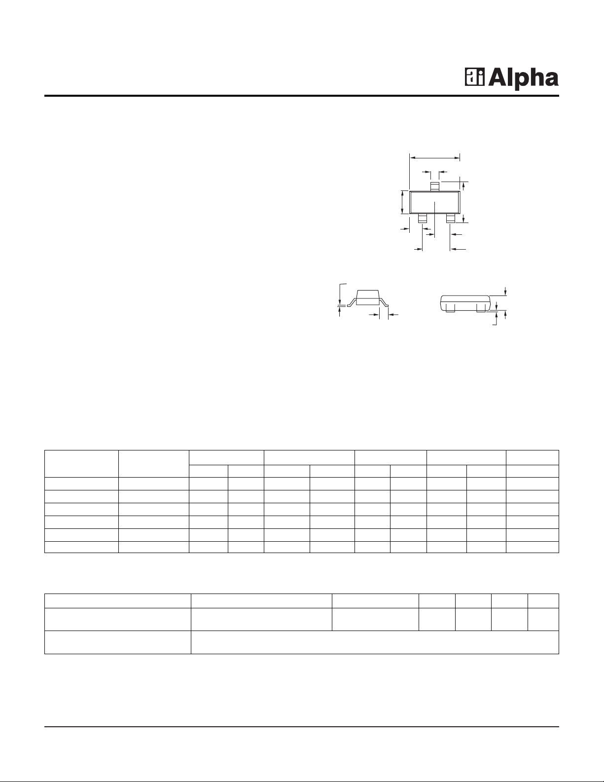
0.045
(1.14 mm)
0.035
(0.89 mm)
0.004 (0.10 mm)
0.0005 (0.01 mm)
0.027 (0.69 mm) REF.
0.007 (0.18 mm)
0.003 (0.08 mm)
0.120 (3.05 mm)
0.110 (2.79 mm)
0.104 (2.64 mm)
0.083 (2.10 mm)
0.055 (1.40 mm)
0.047 (1.19 mm)
0.024 (0.61 mm)
0.018 (0.45 mm)
0.080 (2.03 mm)
0.070 (1.78 mm)
0.018 (0.45 mm)
0.015 (0.38 mm)
3
1
2
0.040 (1.02 mm)
0.037 (0.94 mm)
Features
■ Low Cost SOT-23 Package
■ Series or Shunt Configuration
■ Low DC Current Drain
■ Ideal Switch Building Blocks
■ Pin Diode Replacements
■ High Power Antenna Switches
SOT-23
Description
This group of GaAs control FETs can be used in both
series and shunt configurations.They incorporate on-chip
circuitry that eliminates the need for extra bias
components and minimizes power drain to typically 25 µW.
These features make the device ideal replacements for
PIN diodes, where low DC drain is critical.
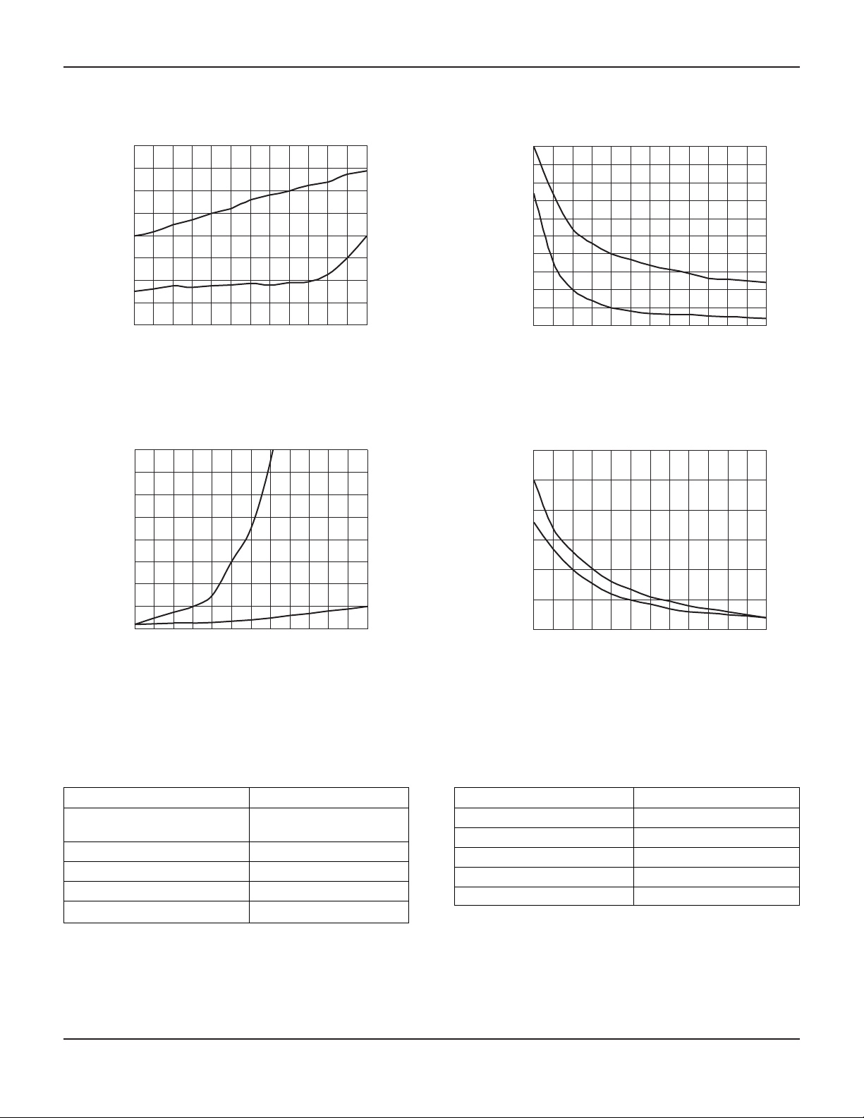
Isolation performance degrades at higher frequencies due
to package parasitics.They can be tuned out in narrow
band applications as shown in the circuit examples on the
following pages.
Parameter Condition Frequency Min. Typ. Max. Unit
Switching Characteristics Rise, Fall (10/90% or 90/10% RF) 6 ns
On, Off (50% CTL to 90/10% RF) 12 ns
Control Voltages V
Low
= 0 to -0.2 V @ 20 µA Max.
V
High
= -5 V @ 50 µA to -9 V @ 200 µA Max.
Operating Characteristics at 25°C (0, -5 V)
1.All measurements made in a 50 Ω system, unless otherwise specified.
2. DC = 300 kHz.
3.R
ON
- resistance in Ω in low impedance state when “0”V is applied to Gate (G).
4. Insertion loss changes by 0.003 dB/°C.
5. Insertion loss and isolation typical values.
6.C
OFF
- capacitance (pF) in high impedance state when -5 V is applied to Gate (G).
Page 2
GaAs IC Control FET Series DC–2.5 GHz AF002C1-39, AF002C4-39
2 Alpha Industries, Inc. [781] 935-5150 • Fax [617] 824-4579 • Email sales@alphaind.com • www.alphaind.com
Specifications subject to change without notice. 3/99A
Insertion Loss vs. Frequency
Series Configuration
0
0.1
0.2
0.3
0.4
0.5
0.6
0.7
0.8
C4
C1
0 0.5 1 1.5 2 2.5 3
Frequency (GHz)
Insertion Loss (dB)
Isolation vs. Frequency
Series Configuration
0 0.5 1 1.5 2 2.5 3
Frequency (GHz)
Isolation (dB)
0
5
10
15
20
25
30
35
40
45
50
C4
C1
Insertion Loss vs. Frequency
Shunt Configuration
0 0.5 1 1.5 2 2.5 3
Frequency (GHz)
Insertion Loss (dB)
0
0.1
0.2
0.3
0.4
0.5
0.6
0.7
0.8
C1
C4
Isolation vs. Frequency
Shunt Configuration
0 0.5 1 1.5 2 2.5 3
Frequency (GHz)
Isolation (dB)
0
5
10
15
20
25
30
C1
C4
Typical Performance Data (0, -5 V)
Characteristic Value
RF Input Power 2 W > 500 MHz 0/-8 V
0.5 W @ 50 MHz 0/-8 V
Control Voltage +0.2 V, -10 V
Operating Temperature -40°C to +85°C
Storage Temperature -65°C to +150°C
Θ
JC
25°C/W
Absolute Maximum Ratings
Note: Exceeding these parameters may cause irreversible damage.
Characteristic Value
RF Input Power 12 W > 450 MHz, 0/-12 V
Control Voltage +0.2, -12 V
Operating Temperature -40°C to +85°C
Storage Temperature -65°C to +150°C
Θ
JC
25°C/W
AF002C1-39 AF002C4-39
Page 3

GaAs IC Control FET Series DC–2.5 GHz AF002C1-39, AF002C4-39
Alpha Industries, Inc. [781] 935-5150 • Fax [617] 824-4579 • Email sales@alphaind.com • www.alphaind.com 3
Specifications subject to change without notice. 3/99A
System Block Diagram
Mobile
Antenna
Phone
Antenna
Diplexer
LNA PA
T/R Switch
Disconnect
Changeover
Switch
From Transmitter
To Receiver
T/R Switch
T/R and Antenna Changeover Switch for Mobile Cellular Systems
D S
G
LT (nH)
10 kΩ
C (pF)
Antenna
G
D
S
T
X
V
CTL
R
X
λ/4
GaAs FET
AF002C
Series
GaAs FET
AF002C
Series
V
CTL
(V) TXto Antenna RXto Antenna
0 Low Loss High Isolation
-5 High Isolation Low Loss
Truth Table for T/R Switch
See next page for positive voltage operation.
V
CTL
(V) Antenna
-5 Connected
0 Isolated
Truth Table for Changeover Switch
See next page for positive voltage operation.
Part Number LT(nH) CT(pF) Freq. (GHz)
AF002C1-39 165 18.8 0.45
AF002C4-39 85 18.8 0.45
AF002C1-39 44 4.7 0.90
AF002C4-39 22 4.7 0.90
Component Values for T/R Switch Circuit
Antenna
C
T
D S
G
To T/R Switch
V
CTL
Changeover Switch SchematicT/R Switch Schematic
Page 4

GaAs IC Control FET Series DC–2.5 GHz AF002C1-39, AF002C4-39
4 Alpha Industries, Inc. [781] 935-5150 • Fax [617] 824-4579 • Email sales@alphaind.com • www.alphaind.com
Specifications subject to change without notice. 3/99A
S D G RF Path
Shunt
-5 Insertion Loss
GND RF
0 Isolation
Series
0 Insertion Loss
RF RF
-5 Isolation
Truth Table
Negative Voltage Operation
Positive Voltage Operation
S D G RF Path
Shunt
0 Insertion Loss
GND RF
V
High
Isolation
Series
0 Isolation
RF RF
V
High
Insertion Loss
CBL - Chose value for lowest impedance at desired operating frequency.
G (0, V
High
)
D S2 1
3
Shunt Configuration
C
T
V
S
10 kΩ
G (0, V
High
)
D S2 1
3
Series Configuration
C
BL
C
BL
V
S
10 kΩ
RF
RFRF
RF
L
T
Positive Voltage Operation
DRAIN (D) SOURCE (S)
GATE (G)
12
3
Pin Out
V
High
= +5 to +9 V (VS= V
High
± 0.2 V).
 Loading...