

Page 1
Fast Starting, ±20,000°/sec
F
V
FEATURES
High vibration rejection over wide frequency
Ultrafast startup: 3 ms
Measurement range extendable to ±50,000°/sec
10,000 g powered shock survivability
Ratiometric to referenced supply
5 V single-supply operation
Z-axis (yaw rate) response
−40°C to +105°C operation
Self-test on digital command
Ultrasmall and light (<0.15 cc, <0.5 gram)
Temperature sensor output
RoHS compliant
APPLICATIONS
Sports equipment
Industrial applications
Platform stabilization
High speed tachometry
Vibration Rejecting Rate Gyro
ADXRS649
GENERAL DESCRIPTION
The ADXRS649 is a complete angular rate sensor (gyroscope)
that uses the Analog Devices, Inc., patented high volume BiMOS
surface-micromachining process to make a complete gyro on
one chip. An advanced, differential, quad sensor design rejects
the influence of linear acceleration, enabling the ADXRS649
to offer rate sensing in harsh environments where shock and
vibration are present.
The output signal, RATEOUT (B1, A2), is a voltage proportional
to the angular rate about the axis normal to the top surface of
the package. The output is ratiometric with respect to a provided
reference supply. An external capacitor is used to set the bandwidth. The measurement range is extendable to ±50,000°/sec
by adding an external resistor.
Low power consumption (3.5 mA) enables very low power
consumption, and ultrafast startup (3 ms) allows for quick
power cycling of the gyro. At 10 samples per second, a pair of
CR2032 coin cells can power the ADXRS649 for three months.
A temperature output is provided for compensation techniques.
Two digital self-test inputs electromechanically excite the sensor
to test proper operation of both the sensor and the signal conditioning circuits. The ADXRS649 is available in a 7 mm × 7 mm ×
3 mm CBGA chip scale package.
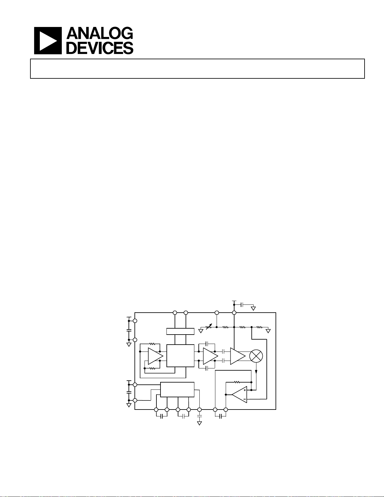
FUNCTIONAL BLOCK DIAGRAM
5V
AV
CC
100nF
AGND
5V
V
DD
100n
Rev. A
Information furnished by Analog Devices is believed to be accurate and reliable. However, no
responsibility is assumed by Anal og Devices for its use, nor for any infringements of patents or ot her
rights of third parties that may result from its use. Specifications subject to change without notice. No
license is granted by implication or otherwise under any patent or patent rights of Analog Devices.
Trademarks and registered trademarks are the property of their respective owners.
PGND
DRIVE
CP1
AMP
ST2 ST1
SELF-TEST
MECHANICAL
SENSOR
CHARGE PUMP
AND VOLTAG E
REGULATO R
CP2 CP3
22nF
CP4 CP5
22nF
5
(ADC REF)
TEMP
V
RATIO
25kΩ
25k
Ω
AT 25° C
AC
AMP
SUMJ RATEOUT
2.2nF
C
OUT
VGA
R
OUT
180kΩ ±1%
100nF
ADXRS649
DEMOD
09573-001
Figure 1.
One Technology Way, P.O. Box 9106, Norwood, MA 02062-9106, U.S.A.
Tel: 781.329.4700 www.analog.com
Fax: 781.461.3113 ©2010–2011 Analog Devices, Inc. All rights reserved.
Page 2

ADXRS649
TABLE OF CONTENTS
Features .............................................................................................. 1
Applications ....................................................................................... 1
General Description ......................................................................... 1
Functional Block Diagram .............................................................. 1
Revision History ............................................................................... 2
Specifications ..................................................................................... 3
Absolute Maximum Ratings ............................................................ 4
Rate Sensitive Axis ....................................................................... 4
ESD Caution .................................................................................. 4
Pin Configuration and Function Descriptions ............................. 5
REVISION HISTORY
3/11—Rev. 0 to Rev. A
Changes to Ordering Guide ............................................................ 1
12/10—Revision 0: Initial Version
Typical Performance Characteristics ..............................................6
Theory of Operation .........................................................................9
Setting the Bandwidth ..................................................................9
Temperature Output and Calibration ...................................... 10
Modifying the Measurement Range ........................................ 10
Null Bias Adjustment ................................................................. 10
Self-Test Function ...................................................................... 10
Continuous Self-Test .................................................................. 10
Outline Dimensions ....................................................................... 11
Ordering Guide .......................................................................... 11
Rev. A | Page 2 of 12
Page 3

ADXRS649
SPECIFICATIONS
All minimum and maximum specifications are guaranteed. Typical specifications are not guaranteed.
T
= −40°C to +105°C, VS = AVCC = VDD = V
A
unless otherwise noted.
Table 1.
Parameter Test Conditions/Comments Min Typ Max Unit
SENSITIVITY1 Clockwise rotation is positive output
Measurement Range2 Full-scale range over specifications range ±20,000 °/sec
Initial and over Temperature
−40°C to +105°C 0.08 0.1 0.12 mV/°/sec
Temperature Drift3 ±2 %
Nonlinearity Best fit straight line 0.1 % of FS
NULL BIAS1
Null Bias −40°C to +105°C 2.4 2.5 2.6 V
Calibrated Null Bias4 −40°C to +105°C ±5 °/sec
Linear Acceleration Effect Any axis 0.1 °/sec/g
Vibration Rectification 40 g rms, 50 Hz to 27 kHz 0.0006 °/sec/g2
NOISE PERFORMANCE
Rate Noise Density TA = 25°C 0.25 °/sec/√Hz
T
A
Resolution Floor TA = 25°C, 1 minute to 1 hour in-run 200 °/hr
FREQUENCY RESPONSE
Bandwidth
5
±3 dB user adjustable up to specification 2000 Hz
Sensor Resonant Frequency 16 18 20 kHz
SELF-TEST1
ST1 RATEOUT Response
ST1 pin from Logic 0 to Logic 1 −1300 °/sec
ST2 RATEOUT Response ST2 pin from Logic 0 to Logic 1 1300 °/sec
ST1 to ST2 Mismatch6
Logic 1 Input Voltage 3.3 V
Logic 0 Input Voltage 1.7 V
Input Impedance To common 40 50 100 kΩ
TEMPERATURE SENSOR1
V
at 25°C Load = 10 MΩ 2.3 2.4 2.5 V
OUT
Scale Factor7 T
Load to V
S
A
25 kΩ
Load to Common 25 kΩ
TURN-ON TIME4 Power on to ±90% of final output, CP5 = 2.2 nF 3 ms
OUTPUT DRIVE CAPABILITY
Current Drive For rated specifications 200 μA
Capacitive Load Drive 1000 pF
POWER SUPPLY
Operating Voltage (VS) 4.75 5.00 5.25 V
Quiescent Supply Current 3.5 mA
TEMPERATURE RANGE
Specified Performance −40 +105 °C
1
Parameter is linearly ratiometric with V
2
Measurement range is the maximum range possible, including output swing range, initial offset, sensitivity, offset drift, and sensitivity drift at 5 V supplies.
3
From +25°C to −40°C or +25°C to +105°C.
4
Based on characterization.
5
Adjusted by external capacitor, C
6
Self-test mismatch is described as (ST2 + ST1)/((ST2 − ST1)/2).
7
Scale factor for a change in temperature from 25°C to 26°C. V
.
RATIO
. Reducing bandwidth below 0.01 Hz does not result in further noise improvement.
OUT
= 5 V, angular rate = 0°/sec, bandwidth = 80 Hz (C
RATIO
= 0.01 μF), I
OUT
= 100 μA, ±1 g,
OUT
= 105°C 0.4 °/sec/√Hz
= 25°C, V
= 5 V 9 mV/°C
RATIO
is ratiometric to V
TEMP
. See the section for more information. Temperature Output and Calibration
RATIO
±2
%
Rev. A | Page 3 of 12
Page 4
ADXRS649
ABSOLUTE MAXIMUM RATINGS
Table 2.
Parameter Rating
Acceleration (Any Axis, 0.5 ms)
Unpowered 10,000 g
Powered 10,000 g
VDD, AV
CC
V
AVCC
RATIO
−0.3 V to +6.0 V
ST1, ST2 AVCC
Output Short-Circuit Duration
Indefinite
(Any Pin to Common)
Operating Temperature Range −55°C to +125°C
Storage Temperature Range −65°C to +150°C
Stresses above those listed under the Absolute Maximum
Ratings may cause permanent damage to the device. This is a
stress rating only; functional operation of the device at these or
any other conditions above those indicated in the operational
section of this specification is not implied. Exposure to absolute
maximum rating conditions for extended periods may affect
device reliability.
Drops onto hard surfaces can cause shocks of greater than
10,000 g and can exceed the absolute maximum rating of the
device. Care should be exercised in handling to avoid damage.
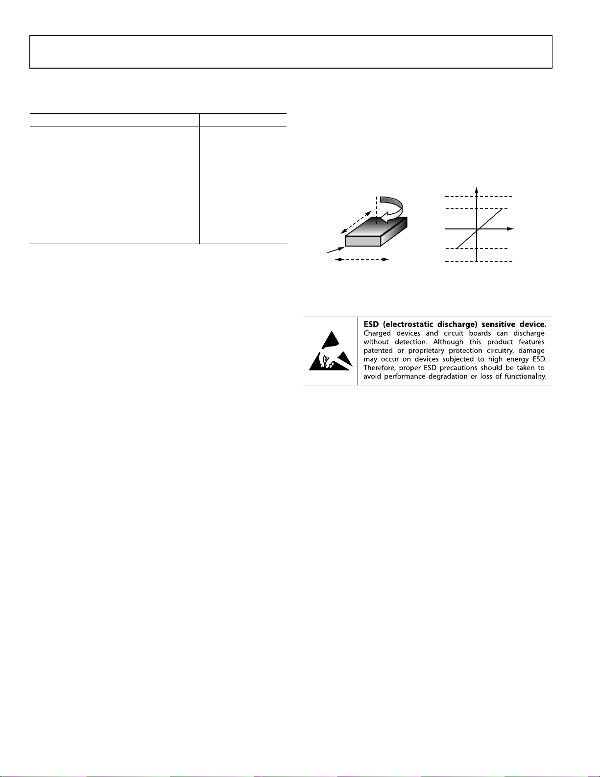
RATE SENSITIVE AXIS
The ADXRS649 is a z-axis rate-sensing device (also called a yaw
rate-sensing device). It produces a positive going output voltage
for clockwise rotation about the axis normal to the package top,
that is, clockwise when looking down at the package lid.
RATE
AXIS
LONGIT UDINAL
AXIS
ABCD G
A1
LATERAL AXIS
Figure 2. RATEOUT Signal Increases with Clockwise Rotation
EF
+
1
A
VCC=5V
7
V
GND
RATIO
RATEOUT
/2
4.75V
RATE IN
0.25V
09573-002
ESD CAUTION
Rev. A | Page 4 of 12
Page 5

ADXRS649
A
V
PIN CONFIGURATION AND FUNCTION DESCRIPTIONS
NC
CP3CP5
SUMJ
CP4
CP1
CP2
AV
CC
RATEOUT
7
6
5
4
3
2
1
9573-003
V
DD
RATIO
PGND
ST1
ST2
TEMP
GND
GF E D C BA
NOTES
1. NC = NO CO NNECT. DO NOT CONNE CT TO T HIS PIN.
Figure 3. Pin Configuration
Table 3. Pin Function Descriptions
Pin No. Mnemonic Description
D6, D7 CP5 High Voltage Filter Capacitor, 2.2 nF.
A6, B7 CP4 Charge Pump Capacitor, 22 nF.
C6, C7 CP3 Charge Pump Capacitor, 22 nF.
A5, B5 CP1 Charge Pump Capacitor, 22 nF.
A4, B4 CP2 Charge Pump Capacitor, 22 nF.
A3, B3 AVCC Positive Analog Supply.
B1, A2 RATEOUT Rate Signal Output.
C1, C2 SUMJ Output Amplifier Summing Junction.
D1, D2 NC Do not connect to these pins.
E1, E2 V
Reference Supply for Ratiometric Output.
RATIO
F1, G2 AGND Analog Supply Return.
F3, G3 TEMP Temperature Voltage Output.
F4, G4 ST2 Self-Test for Sensor 2.
F5, G5 ST1 Self-Test for Sensor 1.
G6, F7 PGND Charge Pump Supply Return.
E6, E7 VDD Positive Charge Pump Supply.
Rev. A | Page 5 of 12
Page 6

ADXRS649
R
A
A
A
A
A
TYPICAL PERFORMANCE CHARACTERISTICS
N > 1000 for all histograms, unless otherwise noted.
0
0
60
–3
–6
–9
TE RESPONSE (d B)
–12
–15
–18
0.1 11
FREQUENCY (kHz)
–30
–60
–90
PHASE (Deg rees)
–120
–150
–180
0
09573-004
Figure 4. Typical Rate and Phase Response vs. Frequency
(C
= 470 pF with a Series RC Low-Pass Filter of 3.3 kΩ and 22 nF)
OUT
4.0
3.5
3.0
2.5
2.0
TE OUT (V)
R
1.5
1.0
0.5
50
40
TION (%)
30
POPUL
20
10
0
2.401
2.434
2.467
2.500
2.533
2.566
2.418
2.451
2.484
2.517
NULL BIAS (V)
2.550
2.583
2.599
09573-007
Figure 7. Null Bias at 25°C
60
50
40
TION (%)
30
POPUL
20
10
0
0 0. 5 1.0 1.5 2.0 2.5 3.0 3.5 4. 0 4.5 5.0
TIME (ms)
Figure 5. Typical Start-Up Behavior at RATEOUT
10000
1000
DEGREES PER HOUR (°)
100
0.01 0.1 1 10 100 1000
TIME (Seconds)
Figure 6. Typical Root Allan Deviation at 25°C vs. Averaging Time
09573-005
09573-006
Rev. A | Page 6 of 12
0
0.081 0.085 0.089 0.093 0.097 0.101 0.105 0.109 0.113 0.117
SENSITIVITY (mV/°/sec)
Figure 8. Sensitivity at 25°C
100
80
60
TION (%)
40
POPUL
20
0
–100
–300
–500
–900
–1100
–1300
–1500
–700
DEGREES PER SECOND (°)
–1700
Figure 9. ST1 Output Change at 25°C (V
RATIO
–1900
= 5 V)
–2100
–2300
09573-008
09573-009
Page 7

ADXRS649
A
A
A
A
z
100
80
60
TION (%)
40
POPUL
20
0
100
300
500
900
1100
1300
1500
700
DEGREES PER SECOND (°)
1700
Figure 10. ST2 Output Change at 25°C (V
70
60
50
40
TION (%)
30
POPUL
20
10
0
–5–4–3–2–1012345
Figure 11. Self-Test Mismatch at 25°C (V
70
MISMATCH (%)
RATIO
RATIO
1900
= 5 V)
2100
= 5 V)
2300
09573-010
09573-011
30
25
20
TION (%)
15
POPUL
10
5
0
2.35 2.37 2.39 2.41 2.43 2.45 2. 47 2.49 2.51 2.53 2.55
OUTPUT (V)
V
TEMP
Figure 13. V
3.3
3.1
2.9
2.7
2.5
OUTPUT (V)
2.3
TEMP
2.1
V
1.9
1.7
1.5
–50 –25 0 25
Figure 14. V
Output over Temperature, 256 Parts (V
TEMP
Output at 25°C (V
TEMP
TEMPERATURE (° C)
= 5 V)
RATIO
50 75 100
RATIO
= 5 V)
09573-013
09573-014
30
25
20
TION (%)
15
POPUL
10
5
0
3.06
3.24
3.42
3.15
3.33
CURRENT CONS UMPTIO N (mA)
3.51
3.60
Figure 12. Current Consumption at 25°C (V
3.69
3.78
3.87
3.96
RATIO
4.05
= 5 V)
4.14
4.23
09573-012
Rev. A | Page 7 of 12
1
ACCELERATI ON
0.1
0.01
AND %/sec
g²/H
0.001
0.0001
100 1000 10000
FREQUENC Y (Hz)
GYRO OUT PUT
Figure 15. Typical Response to 25 g RMS Random Vibration, 50 Hz to 5 kHz
(Sensor Bandwidth = 1 kHz)
09573-015
Page 8

ADXRS649
10
1
0.1
RATEOUT (°/sec Peak)
0.01
0.001
100 1000 10000
VIBRATION INPUT FREQUENCY (Hz)
Figure 16. Typical Response to 10 g RMS Sinusoidal Vibration
(Sensor Bandwidth = 1 kHz)
09573-016
0.5
0.4
0.3
0.2
0.1
0
–0.1
NONLI NEARITY (%)
–0.2
–0.3
–0.4
–0.5
0 5000 10000 15000 20000
ANGULAR RATE (Deg ress per Second)
09573-017
Figure 17. Typical Nonlinearity (Four Typical Devices)
Rev. A | Page 8 of 12
Page 9

ADXRS649
THEORY OF OPERATION
The ADXRS649 operates on the principle of a resonator gyro.
Figure 18 shows a simplified version of one of four polysilicon
sensing structures. Each sensing structure contains a dither
frame that is electrostatically driven to resonance. This produces the necessary velocity element to produce a Coriolis force
when experiencing angular rate. The ADXRS649 is designed to
sense a z-axis (yaw) angular rate.
When the sensing structure is exposed to angular rate, the resulting Coriolis force couples into an outer sense frame, which
contains movable fingers that are placed between fixed pickoff
fingers. This forms a capacitive pickoff structure that senses
Coriolis motion. The resulting signal is fed to a series of gain
and demodulation stages that produce the electrical rate signal
output. The quad sensor design rejects linear and angular
acceleration, including external g-forces and vibration. This is
achieved by mechanically coupling the four sensing structures
such that external g-forces appear as common-mode signals
that can be removed by the fully differential architecture
implemented in the ADXRS649.
The electrostatic resonator requires 13 V to 15 V for operation.
Because only 5 V are typically available in most applications,
a charge pump is included on chip. If an external 13 V to 15 V
supply is available, the two capacitors on CP1 to CP4 can be
omitted, and this supply can be connected to CP5 (Pin D6,
Pin D7). CP5 should not be grounded when power is applied
to the ADXRS649. No damage occurs, but under certain conditions, the charge pump may fail to start up after the ground is
removed without first removing power from the ADXRS649.
SETTING THE BANDWIDTH
External Capacitor C
chip R
resistor to create a low-pass filter to limit the bandwidth
OUT
of the ADXRS649 rate response. The −3 dB frequency set by
and C
R
OUT
f
OUT
f
can be well controlled because R
OUT
is
OUT
= 1/(2 × π × R
during manufacturing to be 180 kΩ ± 1%. Any external resistor
applied between the RATEOUT pin (B1, A2) and the SUMJ pin
(C1, C2) results in
R
= (180 kΩ × R
OUT
In general, an additional filter (in either hardware or software)
is added to attenuate high frequency noise arising from demodulation spikes at the 18 kHz resonant frequency of the gyro. An
RC output filter consisting of a 3.3 kΩ series resistor and 22 nF
shunt capacitor (2.2 kHz pole) is recommended.
is used in combination with the on-
OUT
× C
OUT
EXT
)
OUT
OUT
)/(180 kΩ + R
has been trimmed
)
EXT
X
Y
Z
09573-018
Figure 18. Simplified Gyro Sensing Structure—One Corner
Rev. A | Page 9 of 12
Page 10

ADXRS649
V
TEMPERATURE OUTPUT AND CALIBRATION
It is common practice to temperature-calibrate gyros to improve
their overall accuracy. The ADXRS649 has a temperature proportional voltage output that provides input to such a calibration
method. The temperature sensor structure is shown in Figure 19.
The temperature output is characteristically nonlinear, and any
load resistance connected to the TEMP output results in decreasing
the TEMP output and its temperature coefficient. Therefore,
buffering the output is recommended.
The voltage at TEMP (F3, G3) is nominally 2.5 V at 25°C, and
V
= 5 V. The temperature coefficient is ~9 mV/°C at 25°C.
RATIO
Although the TEMP output is highly repeatable, it has only
modest absolute accuracy.
RATIO
R
FIXEDRTEMP
Figure 19. Temperature Sensor Structure
TEMP
09573-019
MODIFYING THE MEASUREMENT RANGE
The ADXRS649 scale factor can be reduced to extend the
measurement range to as much as ±50,000°/sec by adding a
single 120 kΩ resistor between the RATEOUT and SUMJ pins.
If an external resistor is added between RATEOUT and SUMJ,
C
must be proportionally increased to maintain correct
OUT
bandwidth.
NULL BIAS ADJUSTMENT
The nominal 2.5 V null bias is for a symmetrical swing range at
RATEOUT (B1, A2). However, a nonsymmetric output swing
may be suitable in some applications. Null bias adjustment is
possible by injecting a suitable current to SUMJ (C1, C2). Note
that supply disturbances may reflect some null bias instability.
Digital supply noise should be avoided, particularly in this case.
SELF-TEST FUNCTION
The ADXRS649 includes a self-test feature that actuates each of
the sensing structures and associated electronics in the same
manner, as if subjected to angular rate. The self-test is activated
by standard logic high levels applied to Input ST1 (F5, G5),
Input ST2 (F4, G4), or both. ST1 causes the voltage at RATEOUT
to change by approximately −0.15 V, and ST2 causes an opposite
change of +0.15 V. The self-test response follows the viscosity
temperature dependence of the package atmosphere,
approximately 0.25%/°C.
Activating ST1 and ST2 simultaneously does not damage the
part. ST1 and ST2 are fairly closely matched (±2%), but
actuating both simultaneously may result in a small apparent
null bias shift proportional to the degree of self-test mismatch.
ST1 and ST2 are activated by applying a voltage equal to V
RATIO
to the ST1 pin and the ST2 pin. The voltage applied to ST1 and
ST2 must never be greater than AV
.
CC
CONTINUOUS SELF-TEST
The on-chip integration of the ADXRS649 gives it higher reliability
than is obtainable with any other high volume manufacturing
method. In addition, it is manufactured under a mature BiMOS
process that has field-proven reliability. As an additional failure
detection measure, a power-on self-test can be performed. However, some applications may warrant continuous self-test while
sensing rate. Information about continuous self-test techniques
is also available in the AN-768 Application Note, Using the
ADXRS150/ADXRS300 in Continuous Self-Test Mode.
Rev. A | Page 10 of 12
Page 11

ADXRS649
3
OUTLINE DIMENSIONS
A1 BALL
CORNER
7.05
6.85 SQ
6.70
4.80
BSC SQ
0.80
BSC
76543
21
*
A
B
C
D
E
F
G
A1 CORNER
INDEX AREA
.80 MAX
TOP VIEW
DETAIL A
0.60 MAX
0.25 MIN
SEATING
PLANE
*
BALL A1 IDENTIFIER IS GOLD PLATED AND CONNECTED
TO THE D/A PAD INTERNALLY VIA HOLES.
BOTTOM VIEW
DETAIL A
0.60
0.55
0.50
BALL DIAMETER
3.20 MAX
2.50 MIN
COPLANARITY
0.15
10-26-2009-B
Figure 20. 32-Lead Ceramic Ball Grid Array [CBGA]
(BG-32-3)
Dimensions shown in millimeters
ORDERING GUIDE
Model1 Temperature Range Package Description Package Option
ADXRS649BBGZ-RL –40°C to +105°C 32-Lead Ceramic Ball Grid Array [CBGA] BG-32-3
ADXRS649BBGZ –40°C to +105°C 32-Lead Ceramic Ball Grid Array [CBGA] BG-32-3
EVAL-ADXRS649Z Evaluation Board
1
Z = RoHS Compliant Part.
Rev. A | Page 11 of 12
Page 12

ADXRS649
NOTES
©2010–2011 Analog Devices, Inc. All rights reserved. Trademarks and
registered trademarks are the property of their respective owners.
D09573-0-3/11(A)
Rev. A | Page 12 of 12
 Loading...