

Page 1
High Performance,
V
Data Sheet
FEATURES
Complete rate gyroscope on a single chip
±300°/sec angular rate sensing
High vibration rejection over a wide frequency range
Excellent 25°/hour null offset stability
Internally temperature compensated
2000 g powered shock survivability
SPI digital output with 16-bit data-word
Low noise and low power
3.3 V and 5 V operation
−40°C to +105°C operation
Ultrasmall, light, and RoHS compliant
Two package options
Low cost SOIC_CAV package for yaw rate (Z-axis) response
Innovative ceramic vertical mount package, which can be
oriented for pitch, roll, or yaw response
APPLICATIONS
Rotation sensing medical applications
Rotation sensing industrial and instrumentation
High performance platform stabilization
Digital Output Gyroscope
ADXRS450
GENERAL DESCRIPTION
The ADXRS450 is an angular rate sensor (gyroscope) intended
for industrial, medical, instrumentation, stabilization, and other
high performance applications. An advanced, differential, quad
sensor design rejects the influence of linear acceleration, enabling
the ADXRS450 to operate in exceedingly harsh environments
where shock and vibration are present.
The ADXRS450 uses an internal, continuous self-test architecture. The integrity of the electromechanical system is checked
by applying a high frequency electrostatic force to the sense
structure to generate a rate signal that can be differentiated from
the baseband rate data and internally analyzed.
The ADXRS450 is capable of sensing angular rate of up to
±300°/sec. Angular rate data is presented as a 16-bit word, as
part of a 32-bit SPI message.
The ADXRS450 is available in a cavity plastic 16-lead SOIC
(SOIC_CAV) and an SMT-compatible vertical mount package
(LCC_V), and is capable of operating across both a wide voltage
range (3.3 V to 5 V) and temperature range (−40°C to +105°C).
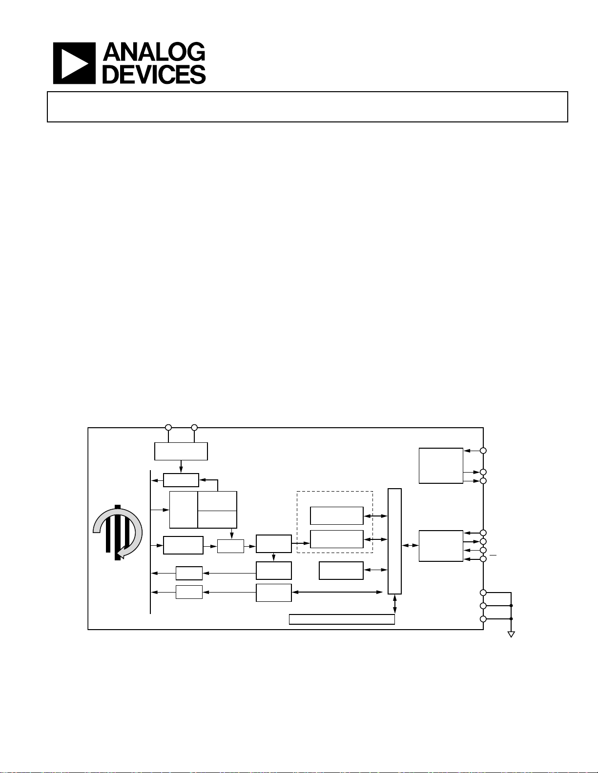
Z-AXIS ANGUL AR
RATE SENSOR
HV DRIVE
PHASE-
LOCKED
LOOP
BAND-PASS
FILTER
Q DAQ
P DAQ
X
CP5
HIGH VOLT AGE
GENERATION
CLOCK
DIVIDER
AMPLITUDE
DETECT
ADC 12
FUNCTIONAL BLOCK DIAGRAM
ADXRS450
ALU
DECIMATION
FILTER
TEMPERATURE
Figure 1.
CALIBRATIO N
FAULT
DETECTIO N
EEPROM
DEMOD
Q FILTER
ST
CONTROL
REGISTERS/MEMORY
LDO
REGULATOR
SPI
INTERFACE
P
DD
DV
DD
AV
DD
MOSI
MISO
SCLK
CS
DV
SS
P
SS
AV
SS
08952-001
Rev. B
Information furnished by Analog Devices is believed to be accurate and reliable. However, no
responsibility is assumed by Anal og Devices for its use, nor for any infringements of patents or ot her
rights of third parties that may result from its use. Specifications subject to change without notice. No
license is granted by implication or otherwise under any patent or patent rights of Analog Devices.
Trademarks and registered trademarks are the property of their respective owners.
One Technology Way, P.O. Box 9106, Norwood, MA 02062-9106, U.S.A.
Tel: 781.329.4700 www.analog.com
Fax: 781.461.3113 ©2011 Analog Devices, Inc. All rights reserved.
Page 2

ADXRS450 Data Sheet
TABLE OF CONTENTS
Features.............................................................................................. 1
Applications....................................................................................... 1
General Description ......................................................................... 1
Functional Block Diagram .............................................................. 1
Revision History ............................................................................... 2
Specifications..................................................................................... 3
Absolute Maximum Ratings............................................................ 4
Thermal Resistance ...................................................................... 4
Rate Sensitive Axis ....................................................................... 4
ESD Caution.................................................................................. 4
Pin Configuration and Function Descriptions............................. 5
Typical Performance Characteristics ............................................. 7
Theory of Operation ........................................................................ 9
Continuous Self-Test.................................................................... 9
Applications Information .............................................................. 10
Calibrated Performance............................................................. 10
Mechanical Considerations for Mounting.............................. 10
Applications Circuits ................................................................. 10
ADXRS450 Signal Chain Timing............................................. 10
SPI Communication Protocol....................................................... 12
Command/Response ................................................................. 12
SPI Communications Characteristics...................................... 13
SPI Applications ......................................................................... 14
SPI Rate Data Format..................................................................... 19
Memory Map and Registers.......................................................... 20
Memory Map .............................................................................. 20
Memory Register Definitions ................................................... 21
Package Orientation and Layout Information............................ 23
Package Marking Codes ............................................................ 25
Outline Dimensions....................................................................... 26
Ordering Guide .......................................................................... 27
REVISION HISTORY
12/11—Rev. A to Rev. B
Changes to the Rate Sensitive Axis Section .................................. 4
Changes to Figure 5.......................................................................... 6
Changes to Figure 28...................................................................... 23
Deleted Figure 31, Renumbered Sequentially ............................ 24
Changes to Back Side Terminals Notation, Figure 34 ............... 26
6/11—Rev. 0 to Rev. A
Changes to Ordering Guide.......................................................... 28
1/11—Revision 0: Initial Version
Rev. B | Page 2 of 28
Page 3

Data Sheet ADXRS450
SPECIFICATIONS
Specification conditions @ TA = T
Table 1.
Parameter Test Conditions/Comments Symbol Min Typ Max Unit
MEASUREMENT RANGE Full-scale range FSR ±300 ±400 °/sec
SENSITIVITY See Figure 2
Nominal Sensitivity 80 LSB/°/sec
Sensitivity Tolerance ±3 %
Nonlinearity1 Best fit straight line 0.05 0.25 % FSR rms
Cross Axis Sensitivity2 ±3 %
NULL
Null Accuracy ±3 °/sec
NOISE PERFORMANCE
Rate Noise Density TA = 25°C 0.015 °/sec/√Hz
LOW-PASS FILTER
Cut-Off (−3 dB) Frequency f0/200, see Figure 6 fLP 80 Hz
Group Delay3 f = 0 Hz tLP 3.25 4 4.75 ms
SHOCK AND VIBRATION IMMUNITY
Sensitivity to Linear Acceleration DC to 5 kHz 0.03 °/sec/g
Vibration Rectification 0.003 °/sec/g2
SELF TEST See Continuous Self-Test section
Magnitude 2559 LSB
Fault Register Threshold Compared to LOCST data 2239 2879 LSB
Sensor Data Status Threshold Compared to LOCST data 1279 3839 LSB
Frequency f0/32 fST 500 Hz
ST Low-Pass Filter
−3 dB Frequency f0/800, see Figure 7 2 Hz
Group Delay3 52 64 76 ms
SPI COMMUNICATIONS
Clock Frequency 8.08 MHz
Voltage Input High
Voltage Input Low
Output Voltage Low MISO, current = 3 mA 0.5 V
Output Voltage High MISO, current = −2 mA PDD − 0.5 V
Pull-Up Current
MEMORY REGISTERS See the Memory Register
Temperature Sensor
Value at 45°C 0 LSB
Scale Factor 5 LSB/°C
Quad, ST, Rate, DNC Registers
Scale Factor 80 LSB/°/sec
POWER SUPPLY
Supply Voltage PDD 3.15 5.25 V
Quiescent Supply Current IDD 6.0 10.0 mA
Turn-On Time Power on to 0.5°/sec of final 100 ms
TEMPERATURE RANGE Independent of package type T
1
Maximum limit is guaranteed through Analog Devices, Inc., characterization.
2
Cross axis sensitivity specification does not include effects due to device mounting on a printed circuit board (PCB).
3
Minimum and maximum limits are guaranteed by design.
MIN
to T
, PDD = 5 V, angular rate = 0°/sec, bandwidth = 80 Hz ±1 g, continuous self-test on.
MAX
CS
MOSI,
MOSI,
CS
CS
, SCLK
CS
, SCLK
, PDD = 3.3 V, CS = 0.75 × PDD
, PDD = 5 V, CS = 0.75 × PDD
Definitions section
0.85 × P
−0.3 P
PDD + 0.3 V
DD
× 0.15 V
DD
50 200 µA
70 300 µA
, T
−40 +105 °C
MIN
MAX
Rev. B | Page 3 of 28
Page 4
ADXRS450 Data Sheet
ABSOLUTE MAXIMUM RATINGS
Table 2.
Parameter Rating
Acceleration (Any Axis, 0.5 ms)
Unpowered 2000 g
Powered 2000 g
Supply Voltage (PDD) −0.3 V to +6.0 V
Output Short-Circuit Duration (Any Pin to
Indefinite
Ground)
Temperature Range
Operating
LCC_V Package −40°C to +125°C
SOIC_CAV Package −40°C to +125°C
Storage
LCC_V Package −65°C to +150°C
SOIC_CAV Package −40°C to +150°C
Stresses above those listed under Absolute Maximum Ratings
may cause permanent damage to the device. This is a stress
rating only; functional operation of the device at these or any
other conditions above those indicated in the operational
section of this specification is not implied. Exposure to absolute
maximum rating conditions for extended periods may affect
device reliability.
THERMAL RESISTANCE
θJA is specified for the worst-case conditions, that is, for a device
soldered in a printed circuit board (PCB) for surface-mount
packages.
Table 3. Thermal Resistance
Package Type θJA θ
16-Lead SOIC_CAV 191.5 25 °C/W
14-Lead Ceramic LCC_V 185.5 23 °C/W
Unit
JC
RATE SENSITIVE AXIS
The ADXRS450 is available in two package options. The
SOIC_CAV package configuration is for applications that
require a z-axis (yaw) rate sensing device.
The vertical mount package (LCC_V) option is for applications
that require rate sensing in the axes parallel to the plane of the
PCB (pitch and roll). See Figure 2 for details.
RATE
AXIS
+
16
RATE
SOIC PACKAGE
9
Figure 2. Rate Signal Increases with Clockwise Rotation
AXIS
Z-AXIS
+
LCC_V PACKAGE
08952-002
The LCC_V package has terminals on two faces; however, the
terminals on the back side are for internal evaluation only and
should not be used in the end application. The terminals on the
bottom of the package incorporate metallization bumps that
ensure a minimum solder thickness for improved solder joint
reliability. These bumps are not present on the back side
terminals and, therefore, poor solder joint reliability can be
encountered if used in the end application. See Figure 34 in the
Outline Dimensions section for a schematic of the LCC_V
package.
ESD CAUTION
Rev. B | Page 4 of 28
Page 5
Data Sheet ADXRS450
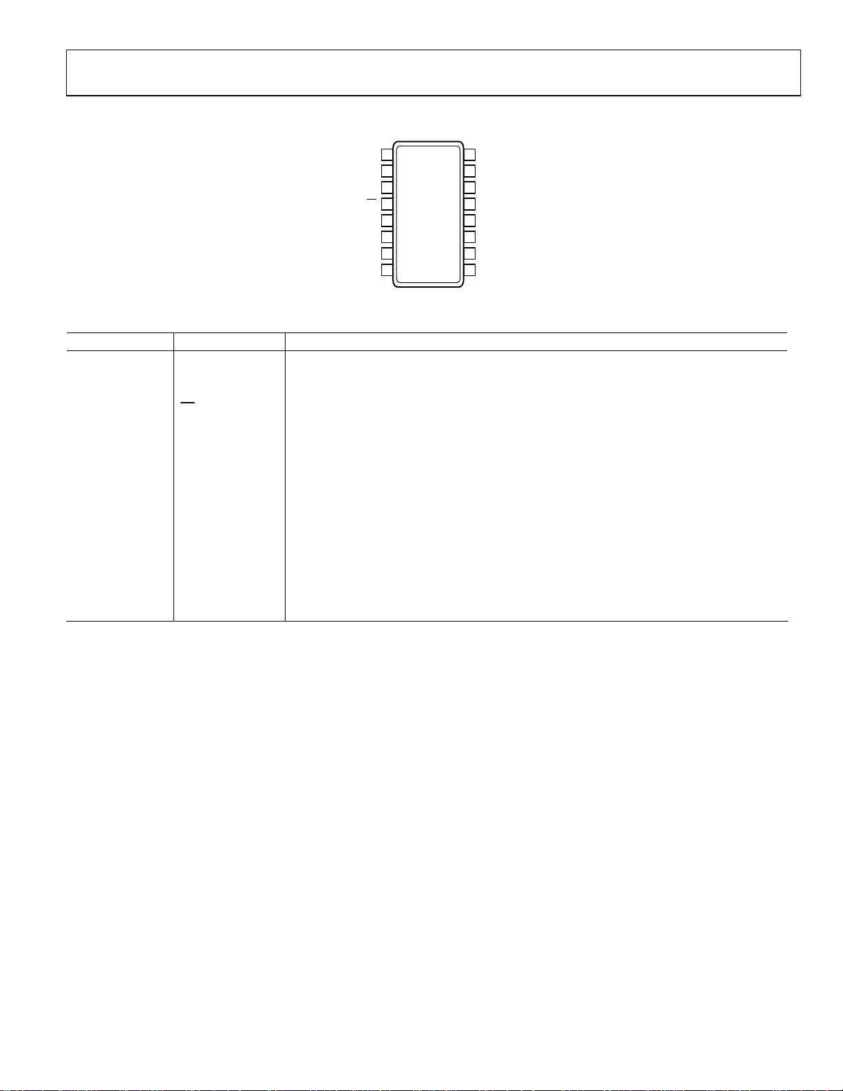
PIN CONFIGURATION AND FUNCTION DESCRIPTIONS
DV
RSVD
RSVD
CS
MISO
P
P
VX
DD
DD
SS
1
2
3
ADXRS450
4
TOP VIEW
(Not to Scale)
5
6
7
8
16
SCLK
15
MOSI
14
AV
DD
13
DV
SS
12
RSVD
11
AV
SS
10
RSVD
9
CP5
08952-003
Figure 3. SOIC_CAV Pin Configuration
Table 4. 14-Lead SOIC_CAV Pin Function Descriptions
Pin No. Mnemonic Description
1 DVDD Digital Regulated Voltage. See Figure 21 for the applications circuit diagram.
2 RSVD Reserved. This pin must be connected to DVSS.
3 RSVD Reserved. This pin must be connected to DVSS.
4
CS
Chip Select.
5 MISO Master In/Slave Out.
6 PDD Supply Voltage.
7 PSS Switching Regulator Ground.
8 VX High Voltage Switching Node. See Figure 21 for the applications circuit diagram.
9 CP5 High Voltage Supply. See Figure 21 for the applications circuit diagram.
10 RSVD Reserved. This pin must be connected to DVSS.
11 AVSS Analog Ground.
12 RSVD Reserved. This pin must be connected to DVSS.
13 DVSS Digital Signal Ground.
14 AVDD Analog Regulated Voltage. See Figure 21 for the applications circuit diagram.
15 MOSI Master Out/Slave In.
16 SCLK SPI Clock.
Rev. B | Page 5 of 28
Page 6
ADXRS450 Data Sheet
PDDPSSMOSI
14 13 12 11 10 9 8
1234567
SS
AV
DVSSCS
DD
DD
AV
MISO
DV
TOP VIEW
(Not to Scale)
VX
RSVD
CP5
SCLK
RSVD
08952-005
Figure 4. LCC_V Pin Configuration
CP5
RSVD
SCLK
DVDDMISO
VX
CS
DV
RSVD
NOTES
1. THE LCC_V PACKAGE HAS TW O TERMI NALS ON T WO FACES; HOWEVER, THE TERMINALS O N THE BACK
SIDE ARE FO R INTERNAL E VALUATIO N ONLY AND SHO ULD NOT BE USED IN THE END APP LICATION. THE
TERMINALS ON THE BOT TOM OF THE PACKAGE INCORPORAT E METALL IZATI ON BUMPS THAT ENSURE A
MINIMUM SOLDER THI CKNESS FOR I MPROVED SOLDER JOI NT RELI ABILIT Y. THESE BUMPS ARE NOT
PRESENT ON T HE BACK SIDE T ERMINALS AND, THEREFO RE, POOR SOLDER JOINT RELI ABILIT Y CAN BE
ENCOUNTERED IF USED IN T HE END APPLICATION. S EE THE OUT LINE DIM ENSIONS S ECTION F OR A
SCHEMATIC O F THE LCC_V PACKAGE.
(Not to Scale)
Figure 5. LCC_V Pin Configuration, Horizontal Layout
SS
AVDDAV
1234567
141312111098
SS
SS
DD
P
P
MOSI
08952-037
Table 5. 14-Lead LCC_V Pin Function Descriptions
Pin No. Mnemonic Description
1 AVSS Analog Ground.
2 AVDD Analog Regulated Voltage. See Figure 22 for the applications circuit diagram.
3 MISO Master In/Slave Out.
4 DVDD Digital Regulated Voltage. See Figure 22 for the applications circuit diagram.
5 SCLK SPI Clock.
6 CP5 High Voltage Supply. See Figure 22 for the applications circuit diagram.
7 RSVD Reserved. This pin must be connected to DVSS.
8 RSVD Reserved. This pin must be connected to DVSS.
9 VX High Voltage Switching Node. See Figure 22 for the applications circuit diagram.
10
CS
Chip Select.
11 DVSS Digital Signal Ground.
12 MOSI Master Out/Slave In.
13 PSS Switching Regulator Ground.
14 PDD Supply Voltage.
Rev. B | Page 6 of 28
Page 7
Data Sheet ADXRS450
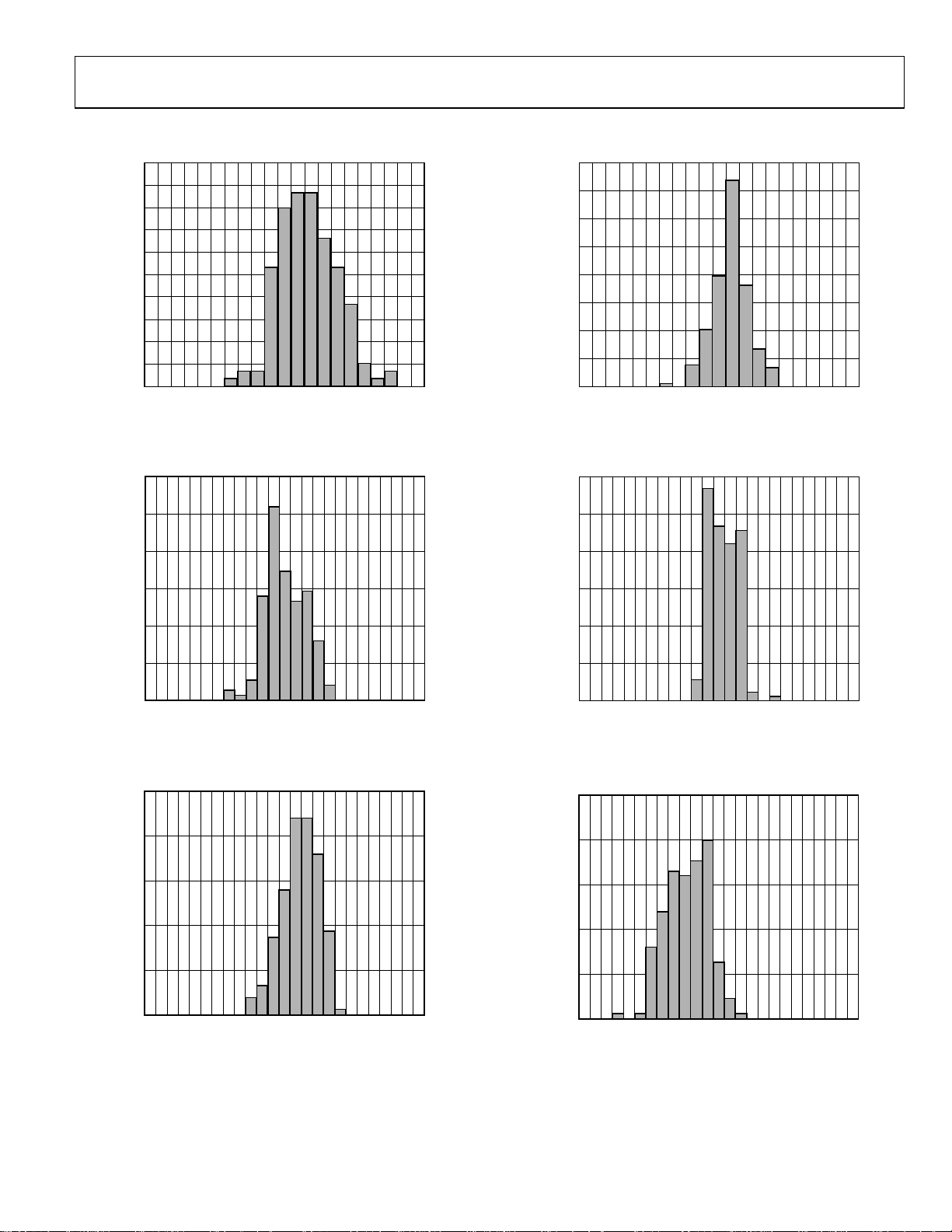
TYPICAL PERFORMANCE CHARACTERISTICS
0.20
0.18
0.16
0.14
0.12
0.10
0.08
% OF POPULATION
0.06
0.04
0.02
0
–1.6
–2.0
–1.2
–0.8
NULL ERROR (° /sec)
0
–0.4
0.8
0.4
1.6
1.2
2.0
08952-006
Figure 6. SOIC_CAV Null Error @ 25°C
0.30
0.40
0.35
0.30
0.25
0.20
0.15
% OF POPULATION
0.10
0.05
0
–2.0 –1.6 –1.2 –0.8 –0.4 0 2.01.61.20.80.4
NULL ERROR (° /sec)
Figure 9. LCC_V Null Error @ 25°C
0.30
08952-009
0.25
0.20
0.15
0.10
% OF POPULATION
0.05
0
–2.5
–2.0
–1.5
–1.0
–3.0
–0.5
NULL DRIFT ERROR (°/ sec)
Figure 7. SOIC_CAV Null Drift over Temperature
0.25
0.20
0.15
0.10
% OF POPULATION
0.05
0.25
0.20
0.15
0.10
% OF POPULATION
0.05
0
0.5
1.0
1.5
2.0
2.5
3.0
08952-007
0
–2.5
–2.0
–3.0
–1.5
NULL DRIFT ERROR (° /sec)
0
–0.5
–1.0
1.5
1.0
–0.5
3.0
2.5
2.0
08952-010
Figure 10. LCC_V Null Drift over Temperature
0.25
0.20
0.15
0.10
% OF POPULATION
0.05
0
–3.0
–2.5
–2.0
–1.5
CHANGE IN SENSITIVITY (%)
0
–1.0
–0.5
Figure 8. SOIC_CAV Sensitivity Error @ 25°C
0.5
1.0
1.5
2.0
2.5
3.0
08952-008
0
–3.0
–2.5
–2.0
–1.5
CHANGE IN SENSITIVITY (%)
0
0.5
1.0
1.5
2.0
2.5
–1.0
–0.5
3.0
08952-029
Figure 11. LCC_V Sensitivity Error @ 25°C
Rev. B | Page 7 of 28
Page 8
ADXRS450 Data Sheet
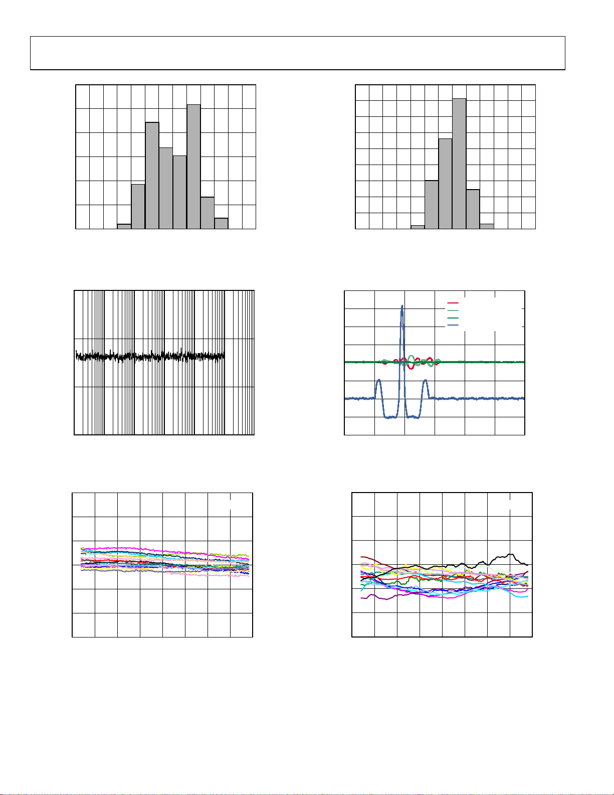
R
0.30
0.25
0.20
0.15
0.10
% OF POPULATION
0.05
0
–3
–2
–1
DRIFT (%)
1
0
Figure 12. SOIC_CAV Sensitivity Drift over Temperature
1
0.1
3
2
08952-030
0.45
0.40
0.35
0.30
0.25
0.20
0.15
% OF POPULATION
0.10
0.05
0
–3
–2
CHANGE IN SENSITIVITY (%)
0
–1
Figure 15. LCC_V Sensitivity Drift over Temperature
40
30
20
10
DUT1
DUT2
DUT AVERAGE (°/s)
REF
3
2
1
08952-033
60
50
40
30
/Hz)
2
(g
0.01
0.001
065k4k3k2k1k
VIBRATION F REQUENCY (Hz)
k
Figure 13. Typical Response to Random Vibration, 15 g rms, 50 Hz to 5 kHz
3
N = 16
2
1
0
–1
NULL OUTPUT ERRO
–2
–3
–50 1109070503010–10–30
DUT TEMPERATURE (°C)
Figure 14. Null Output over Temperature, Device Soldered on PCB
0
–10
GYRO OUTPUT (°/s)
–20
–30
–40
0.1 0.15 0.20 0.25 0.30 0.35 0.40
08952-031
TIME (sec)
20
10
0
–10
–20
INPUT ACCELERAT ION (g)
08952-034
Figure 16. Typical Shock Response
3
N = 16
2
1
0
–1
–2
SENSITIVITY OVER TEMPERATURE ERROR
–3
08952-032
–50 1109070503010–10–30
DUT TEMPERATURE (°C)
08952-035
Figure 17. Sensitivity over Temperature, Device Soldered to PCB
Rev. B | Page 8 of 28
Page 9
Data Sheet ADXRS450
S
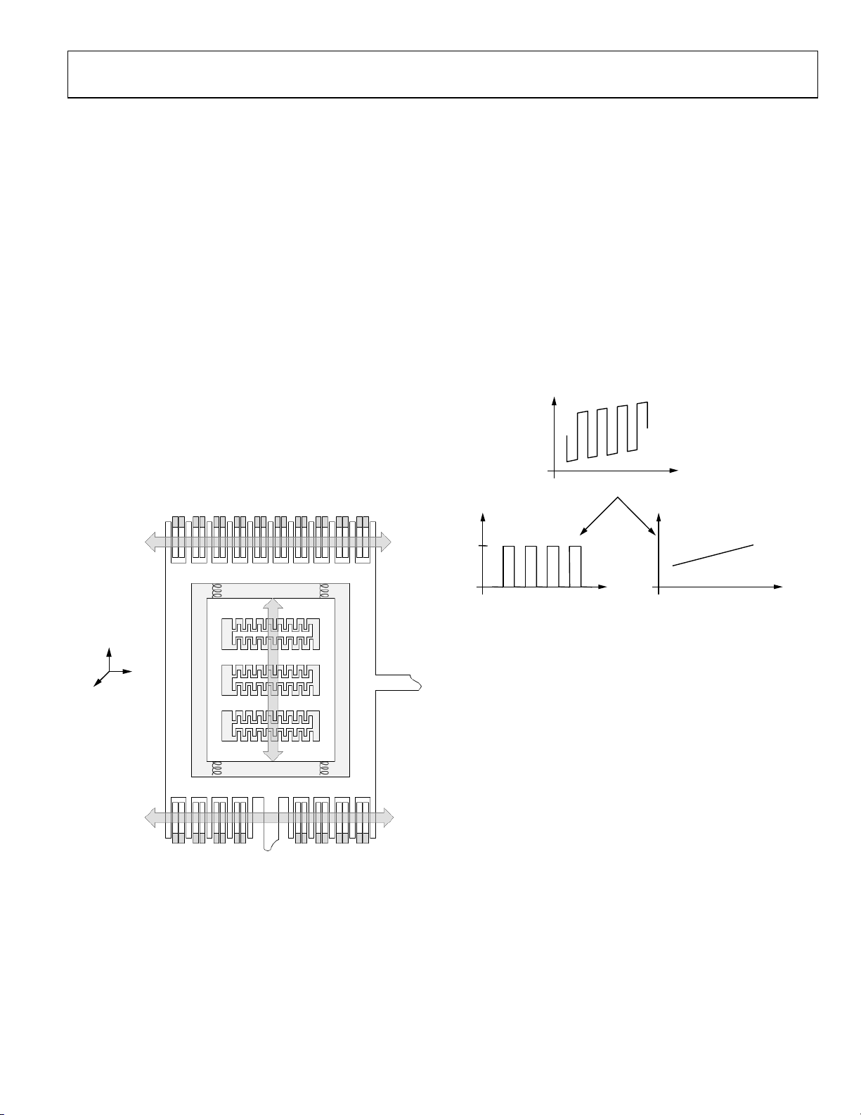
THEORY OF OPERATION
The ADXRS450 operates on the principle of a resonator gyroscope. A simplified version of one of four polysilicon sensing
structures is shown in Figure 18. Each sensing structure contains
a dither frame that is electrostatically driven to resonance. This
produces the necessary velocity element to produce a Coriolis
force when experiencing angular rate. In the SOIC_CAV package,
the ADXRS450 is designed to sense a z-axis (yaw) angular rate;
whereas the vertical mount package (LCC_V) orients the device
such that it can sense pitch or roll angular rate on the same PCB.
When the sensing structure is exposed to angular rate, the
resulting Coriolis force couples into an outer sense frame,
which contains movable fingers that are placed between fixed
pickoff fingers. This forms a capacitive pickoff structure that
senses Coriolis motion. The resulting signal is fed to a series of
gain and demodulation stages that produce the electrical rate
signal output. The quad sensor design rejects linear and angular
acceleration, including external g-forces and vibration. This is
achieved by mechanically coupling the four sensing structures
such that external g-forces appear as common-mode signals
that can be removed by the fully differential architecture
implemented in the ADXRS450.
CONTINUOUS SELF-TEST
The ADXRS450 gyroscope uses a complete electromechanical
self-test. An electrostatic force is applied to the gyroscope frame,
resulting in a deflection of the capacitive sense fingers. This
deflection is exactly equivalent to deflection that occurs as a
result of external rate input. The output from the beam structure is
processed by the same signal chain as a true rate output signal,
providing complete coverage of the electrical and mechanical
components.
The electromechanical self-test is performed continuously during
operation at a rate higher than the output bandwidth of the
device. The self-test routine generates equivalent positive and
negative rate deflections. This information can then be filtered
with no overall effect on the demodulated rate output.
RATE SIGNAL WITH
CONTINUOUS S ELF TES T SIGNAL .
X
Y
Z
Figure 18. Simplified Gyroscope Sensing Structure
The resonator requires 22.5 V (typical) for operation. Because
only 5 V is typically available in most applications, a switching
regulator is included on chip.
ELF TEST AMPLIT UDE. INTERNAL LY
COMPARED TO THE SPECIFICATION
TABLE LI MITS.
Figure 19. Continuous Self-Test Demodulation
LOW FRE QUENCY RATE I NFORMATI ON.
The difference amplitude between the positive and negative
self-test deflections is filtered to 2 Hz, and it is continuously
monitored and compared to hardcoded self-test limits. If the
measured amplitude exceeds these limits (listed in Tab l e 1 ), one
of two error conditions asserts depending on the magnitude of
self-test error. For less severe self-test error magnitudes, the CST
bit of the fault register is asserted; however, the status bits (ST[1:0])
in the sensor data response remain set to 0b01 for valid sensor
data. For more severe self-test errors, the CST bit of the fault register is asserted, and the status bits (ST[1:0]) in the sensor data
response are set to 0b00 for invalid sensor data. Ta b le 1 lists the
08952-011
thresholds for both of these failure conditions. If desired, the user
can access the self-test information by issuing a read command to
the self-test memory register (Address 0x04). For more information about error reporting, see the SPI Communication Protocol
section.
08952-012
Rev. B | Page 9 of 28
Page 10

ADXRS450 Data Sheet
V
G
APPLICATIONS INFORMATION
CALIBRATED PERFORMANCE
Each ADXRS450 gyroscope uses internal EEPROM memory to
store its temperature calibration information. The calibration
information is encoded into the device during factory test. The
calibration data is used to perform offset, gain, and self-test corrections over temperature. By storing this information internally,
it removes the burden from the customer of performing system
level temperature calibration.
MECHANICAL CONSIDERATIONS FOR MOUNTING
Mount the ADXRS450 in a location close to a hard mounting
point of the PCB to the case. Mounting the ADXRS450 at an
unsupported PCB location (that is, at the end of a lever, or in
the middle of a trampoline), as shown in Figure 20, can result in
apparent measurement errors because the gyroscope is subject
to the resonant vibration of the PCB. Locating the gyroscope
near a hard mounting point helps to ensure that any PCB resonances at the gyroscope are above the frequency at which harmful
aliasing with the internal electronics can occur. To ensure that
aliased signals do not couple into the baseband measurement
range, design the module wherein the first system level resonance
occurs at a frequency higher than 800 Hz.
GYROSCOPE
PCB
MOUNTING POINTS
Figure 20. Incorrectly Placed Gyroscope
8952-013
APPLICATIONS CIRCUITS
Figure 21 and Figure 22 show the recommended application
circuits for the ADXRS450 gyroscope. These application circuits
provide a connection reference for the available package types.
Note that DV
ground through 1 F capacitors; do not connect these supplies
together. Additionally, an external diode and inductor must be
connected for proper operation of the internal shunt regulator.
These components (listed in Tabl e 6 ) allow for the internal resonator drive voltage to reach its required level, as listed in the
Specifications section.
Table 6. Internal Shunt Regulator Components
Component Qty. Description
Inductor 1 470 H
Diode 1 >24 V breakdown voltage
Capacitor 3 1 F
Capacitor 1 100 nF
, AVDD, and PDD are individually connected to
DD
1µF
GND
3.3V TO 5V
1µF
470µH
GND
Figure 21. Recommended Applications Circuit, SOIC_CAV Package
1µF
1µF
100nF
ND
Figure 22. Recommended Applications Circuit, Ceramic LCC_V Package
ADXRS450 SIGNAL CHAIN TIMING
The ADXRS450 primary signal chain is shown in Figure 23; it is
the series of necessary functional circuit blocks through which
the rate data is generated and processed. This sequence of electromechanical elements determines how quickly the device is capable
of translating an external rate input stimulus into an SPI word
to be sent to the master device. The group delay, which is a function of the filter characteristic, is the time required for the output
of the low-pass filter to be within 10% of the external rate input,
and is seen to be ~4 ms. Additional delay can be observed due
to the timing of SPI transactions and the population of the rate
data into the internal device registers. Figure 23 anatomizes this
delay, wherein the delay through each element of the signal chain
is presented.
116
DV
DD
RSVD
RSVD
CS
MISO
P
DD
P
SS
VX
>24V BREAKDOWN
TOP VIEW
114
AV
SS
AV
DD
MISO
DV
DD
SCLK
CP5
RSVD
DIODE
>24V BREAKDOWN
DIODE
MOSI
DV
RSVD
P
P
CS
VX
SCLK
MOSI
AV
DV
RSVD
AV
RSVD
CP5
DD
SS
SS
DD
SS
SS
GND
1µF
3.3
GND
1µF
100nF
TO 5V
470µH
GND
08952-014
08952-015
Rev. B | Page 10 of 28
Page 11

Data Sheet ADXRS450
Z
The transfer function for the rate data LPF is given as
2
−
64
⎡
1
⎢
⎣
⎤
−
Z
⎥
−
1
−
1
Z
⎦
where:
T =
f
0
11
=
(typ)kHz16
PRIMARY SIGNAL CHAIN
The transfer function for the continuous self-test LPF is given as
1
1
−
6364
−
where:
16
T =
=
f
0
(typ)ms1
4ms
GROUP DELAY
SPI
<2.2ms
DELAY
08952-016
Z-AXIS ANGULAR
RATE SENSOR
<5µs
DELAY
BAND-PASS
FILTER
<5µs
DELAY
ADC 12
<5µs
DELAY
DEMOD
ARITHMETI C
LOGIC UNIT
RATE DATA
LPF
CONTINUOUS
SELF-TEST
LPF
<64ms
GROUP DELAY
TRANSACTION
REGISTERS/MEMORY
Figure 23. Primary Signal Chain and Associated Delays
Rev. B | Page 11 of 28
Page 12

ADXRS450 Data Sheet
6
SPI COMMUNICATION PROTOCOL
COMMAND/RESPONSE
Input/output is handled through a 32-bit, command/response
SPI interface. The command set and the format for the interface
is defined as follows:
Clock phase = clock polarity = 0
Additionally, the device response to the initial command is
0x00000001. This prevents the transmission of random data to
the master device upon the initial command/response exchange.
CS
Table 7. SPI Signals
Signal Symbol Description
Serial Clock SCLK
Chip Select
Master Out
CS
MOSI
Slave In
Master In
MISO
Slave Out
Exactly 32 clock cycles during CS
Active low
Data sent to the gyroscope device
from the main controller
Data sent to the main controller
from the gyroscope
active
SCLK
MOSI
MISO
32 CLOCK
CYCLES
COMMAND N
RESPONSE N – 1
Figure 24. SPI Protocol
32 CLOCK
CYCLES
COMMAND N + 1
RESPONSE N
08952-017
Table 8. SPI Commands
Bit
Command
Sensor
Data
Read 1 0 0 SM2 SM1 SM0 A8 A7 A6 A5 A4 A3 A2 A1 A0 P
Write 0 1 0 SM2 SM1 SM0 A8 A7 A6 A5 A4 A3 A2 A1 A0 D15 D14 D13 D12 D11 D10 D9 D8 D7 D6 D5 D4 D3 D2 D1 D0 P
31 30 29 28 27 26 25 24 23 22 21 20 19 18 17 16 15 14 13 12 11 10 9 8 7
SQ1 SQ0 1 SQ2 CHK P
5 4 3 2 1 0
Table 9. SPI Responses
Bit
Command
Sensor
Data
Read 0 1 0 P0 1 1 1 0 SM2 SM1 SM0 D15 D14 D13 D12 D11 D10 D9 D8 D7 D6 D5 D4 D3 D2 D1 D0 P1
31 30 29 28 27 26 25 24 23 22 21 20 19 18 17 16 15 14 13 12 11 10 9 8 7 6 5 4 3 2 1 0
SQ2 SQ1 SQ0 P0 ST1 ST0 D15 D14 D13 D12 D11 D10 D9 D8 D7 D6 D5 D4 D3 D2 D1 D0 PLL Q NVM POR PWR CST CHK P1
Write 0 0 1 P0 1 1 1 0 SM2 SM1 SM0 D15 D14 D13 D12 D11 D10 D9 D8 D7 D6 D5 D4 D3 D2 D1 D0 P1
R/W
Error
0 0 0 P0 1 1 1 0 SM2 SM1 SM0 0 0 SPI RE DU PLL Q NVM POR PWR CST CHK P1
Rev. B | Page 12 of 28
Page 13

Data Sheet ADXRS450
SPI COMMUNICATIONS CHARACTERISTICS
Note the following conditions for Table 10 :
• All minimum and maximum timing values are guaranteed
through characterization.
• All timing is shown with respect to 10% V
the actual delivered voltage waveform.
• All minimum and maximum timing values are valid for
3.0 V ≤ V
≤ 5.5 V.
DD
• Capacitive load for all signals is assumed to be ≤80 pF.
• Ambient temperature is −40°C ≤ T
≤ +105°C.
A
• MISO pull-up of 47 kΩ or 110 µA.
• Sequential transfer increases to 17 ms following any write
operation limited by the EEPROM.
and 90% of
DD
Table 10. SPI Command/Response Timing Characteristics
Symbol Description Min Max Unit
f
OP
t
SCLKH
t
SCLKL
t
SCLK
t
F
t
R
t
SU
t
HIGH
t
A
t
V
t
LAG
t
DIS
t
LEAD
t
LAG
t
D
f
0
SPI operating
8.08 MHz
frequency
Clock (SCLK)
1/2t
− 13 ns
SCLK
high time
Clock (SCLK) low
1/2t
− 13 ns
SCLK
time
SCLK period 123.7 ns
Clock (SCLK) fall
5.5 13 ns
time
Clock (SCLK) rise
5.5 13 ns
time
Data input
37 ns
(MOSI) setup
time
Data input
49 ns
(MOSI) hold time
Data output
20 ns
(MISO) access
time
Data output
20 ns
(MISO) valid after
SCLK
Data output
0 ns
(MISO) lag time
Data output
40 ns
(MISO) disable
time
1/2t
Enable (CS) lead
time
Enable (CS) lag
ns
SCLK
ns
1/2t
SCLK
time
Sequential
0.1 ms
transfer delay
Gyroscope
13 19 kHz
resonant
frequency
Rev. B | Page 13 of 28
Page 14

ADXRS450 Data Sheet
K
SPI APPLICATIONS
Device Data Latching
To allow for rapid acquisition of data from the ADXRS450,
device data latching has been implemented in the design, as shown
in Figure 26. Upon the assertion of chip select (
present in the device is latched into memory. When the full
MOSI command has been received, and
CS
t
LEAD
SCK
CS
), the data
CS
deasserted, the
t
SCLK
t
SCLKHtSCLKL
t
F
appropriate data is shifted into the SPI port registers in preparation for the next sequential command/response exchange. This
allows for an exceedingly fast sequential transfer delay of 0.1 ms
Tabl e 10
(see ). As a design precaution, note that the transmitted
data is only as recent as the sequential transmission delay implemented by the system. Conditions that result in a sequential
transfer delay of several seconds cause the next sequential device
response to contain data that is several seconds old.
t
t
R
LAG
t
D
SCL
MOSI
CS
t
A
MISO
MOSI
DEVICE DATA IS LAT CHED AFTER THE
ASSERTION O F CS. LAT CHED DATA IS
TRANSMITT ED DURING THE NEXT
SEQUENTIAL COMMAND/RESP ONSE
EXCHANGE.
32 CLOCK
CYCLES
COMMAND N
0x…
MSB
t
HIGH
t
SU
MSB
t
LAG
t
V
Figure 25. SPI Timings
32 CLOCK
COMMAND N + 1
CYCLES
0x…
t
DIS
LSB
LSB
32 CLOCK
CYCLES
COMMAND N + 2
0x…
08952-018
MISO
RESPONSE N – 1
0x00000001
RESPONSE N
0x…
RESPONSE N + 1
0x…
8952-019
Figure 26. Device Data Latching
Rev. B | Page 14 of 28
Page 15

Data Sheet ADXRS450
Command/Response—Bit Definitions
Table 11. Quick Guide—Bit Definitions for SPI Interface
Bit Description
SQ2 to SQ0 Sequence bits (from master)
SM2 to SM0 Sensor module bits (from master)
A8 to A0 Register address
D15 to D0 Data
SPI SPI command/response
ST1 to ST0 Status bits
P Command odd parity
P0 Response, odd parity, Bits[31:16]
P1 Response, odd parity, Bits[31:0]
RE Request error
DU Data unavailable
SQ2 to SQ0
This field provides the system with a means of synchronizing
the data samples that are received from multiple sensors. To
facilitate correct synchronization, the ADXRS450 gyroscope
includes the SQ[2:0] field in the response sequence as it was
received in the request.
SM2 to SM0
Sensor module bits from master device. These bits have not
been implemented in the ADXRS450, and are hardcoded to be
000 for all occurrences.
A8 to A0
The A8 to A0 bits represent the memory address from which
device data is being read, or to which information is to be written.
These bits should only be supplied by the master when the
memory registers are being accessed, and are ignored for all
sensor data requests. Refer to the Memory Register Definitions
section for a complete description of the available memory
registers.
D15 to D0
16-bit device data that can contain any of the following:
• Master—data to be written to a memory register as
specified in the A8 to A0 section.
• Slave—sensor rate output data.
• Slave—device data read from the memory register
specified in the A8 to A0 section, as well as the data from
the next sequential register.
• Slave—for a write command, the 16-bit data that is written
to the specified memory register reflects back to the master
device for correlation.
SPI
The SPI bit sets when any of the following occurs: either too
many/not enough bits are transmitted, or the message from the
control module contains a parity error. Additionally, any error
during a sensor data request results in the device issuing a
read/write error.
ST1 to ST0
The status bits (ST1 and ST0) are used to signal to the master
device the type of data contained in the response message. The
status bits are decoded as listed in Tabl e 1 2 .
Table 12. Status Bit Code Definitions
ST1:ST0 Content in Bits[D15:D0]
00 Error data for sensor data response
01 Valid sensor data
10 Sensor self-test data
11 Read/write response
There are two independent conditions that can result in the ST
bits being set to 0b00 during a sensor data response: self-test or
PLL. The self-test response is sufficiently different from its nominal
value. Refer to the Specifications section for the appropriate limits.
When the sensor data response is a PLL, the PLL fault is active.
P
A parity bit (P) is required for all master-to-slave data transmissions. Communications protocol requires one parity bit to achieve
odd parity for the entire 32-bit command. Bits that are in don’t
care positions remain factored into the parity calculation.
P0
P0 is the parity bit that establishes odd parity for Bits[31:16] of
the device response.
P1
P1 is the parity bit that establishes odd parity for the entire
32-bit device response.
RE
RE is the communications error bit transmitted from the
ADXRS450 device to the control module. Request errors (RE)
can occur when
• An invalid command is sent from the control module.
• The read/write command specifies an invalid memory
register.
• The write command attempted to a nonwriteable memory
register.
DU
As expressed in Ta bl e 10 , the sequential transfer delay for
writing data to a memory register (for example, DNC0) results
in a sequential transfer delay of 0.1 ms. If a successive write
command is issued to the device prior to the completion of the
sequential transfer delay, the command is ignored and the device
issues a data unavailable (DU) error response. However, a read
command or sensor data request can be issued after a sequential
transfer delay of only 10 µs is observed. Regardless of the commands that are subsequently issued to the device, when a write
procedure has been initiated, the operation proceeds through to
completion (requiring 17 ms).
Rev. B | Page 15 of 28
Page 16

ADXRS450 Data Sheet
Fault Register Bit Definitions
This section describes the bits available for signaling faults to
the user. The individual bits of the fault register are updated
asynchronously depending on their respective detection criteria;
however, it is recommended that the fault register be read at a
rate of at least 250 Hz. When asserted, the individual status bit
does not deassert until it is read by the master device. If the
error persists after a fault register read, the status bit immediately
reasserts, and remains asserted until the next sequential command/
response exchange. The full fault register is appended to every
sensor data request. It can also be accessed by issuing a read
command to Register 0x0A.
Table 13. Quick Guide—Fault Register Bit Definitions
Bit Name Description
PLL PLL failure
Q Quadrature error
NVM Nonvolatile memory fault (NVM)
POR Power-on reset failed to initialize
UV Regulator undervoltage
Amp Amplitude detection failure
PWR Power regulation failed: overvoltage/undervoltage
CST Continuous self-test failure
CHK Check: generate faults
OV Regulator overvoltage
Fail Failure that sets the ST[1:0] bits to 0b00
PLL
PLL is the bit indicating that the device has had a failure in the
phase-locked loop functional circuit block. This occurs when
the PLL has failed to achieve sync with the resonator structure.
If the PLL status flag is active, the ST bits of the sensor data
response are set to 0b00, indicating that the response contains
potentially invalid rate data.
Q
A Q fault can be asserted based on two independent quadrature
calculations. Located in the quad memory (Register 0x08) is a
value corresponding to the total instantaneous quadrature present
in the device. If this value exceeds 4096 LSB, a Q fault is issued.
Because quadrature build-up can contribute to an offset error,
the ADXRS450 has integrated methods for dynamically cancelling
the effects of quadrature. An internal quadrature accumulator
records the amount of quadrature correction performed by the
ADXRS450. Excessive quadrature is associated with offset errors.
A Q fault is issued when the quadrature error (Q) present in the
device has contributed to an equivalent of 4°/sec (typical) of rate
offset.
NVM
An NVM error transmits to the control module when the
internal NVM data fails a checksum calculation. This check is
performed once every 50 µs, and does not include the DNC0 or
PID memory registers.
POR
An internal check is performed at the time of device startup to
ensure that the volatile memory of the device is functional. This
is accomplished by programming a known value from the device
ROM into a volatile memory register. This value is then continuously compared to the known value in ROM every 1 µs for the
duration of device operation. If the value stored in the volatile
memory changes, or does not match the value stored in ROM,
the POR error flag is asserted. The value stored in ROM is
rewritten to the volatile memory upon a device power cycle.
PWR
The device performs a continuous check of the internal 3 V
regulated voltage level. If either an overvoltage (OV) or undervoltage (UV) fault is asserted, then the power (PWR) bit is also
asserted. This condition occurs if the regulated voltage is observed
to be either above 3.3 V or below 2.77 V. An internal low-pass
filter removes high frequency glitching effects to prevent the
PWR bit from asserting unnecessarily. To determine if the fault
is a result of an overvoltage or undervoltage condition, the OV
and UV fault bits must be analyzed.
CST
The ADXRS450 is designed with continuous self-test (CST)
functionality. Measured self-test amplitudes are compared
against the limits presented in Tab l e 1. Deviations from this
value are what result in reported self-test errors. There are two
thresholds for a self-test failure.
• Self-test value > ±512 LSB from nominal results in an
assertion of the self-test flag in the fault register.
• Self-test value > ±1856 LSB from nominal results in both
an assertion of the self-test flag in the fault register as well
as setting the ST[1:0] bits to 0b00, indicating that the rate
data contained in the sensor data response is potentially
invalid.
CHK
The control module transmits the check (CHK) bit to the
ADXRS450 as a method of generating faults. By asserting
the CHK bit, the device creates conditions that result in the
generation of all faults represented through the fault register.
For example, the self-test amplitude is deliberately altered to
exceed the fault detection threshold, resulting in a self-test
error. In this way, the device is capable of checking both its
ability to detect a fault condition, as well as its ability to report
that fault to the control module.
The fault conditions are initiated nearly simultaneously; however,
the timing for receiving fault codes when the CHK bit is asserted
is dependent upon the time required to generate each unique fault.
It takes no more than 50 ms for all of the internal faults to be generated and for the fault register to be updated to reflect the condition
of the device. Until the CHK bit is cleared, the status bits (ST[1:0])
are set to 0b10, indicating that the data should be interpreted
by the control module as self-test data. After the CHK bit is
Rev. B | Page 16 of 28
Page 17

Data Sheet ADXRS450
deasserted, the fault conditions require an additional 50 ms to
decay, and the device to return to normal operation.
OV
The overvoltage (OV) fault bit asserts if the internally regulated
voltage (nominally 3 V) is observed to exceed 3.3 V. This measurement is low-pass filtered to prevent artifacts such as noise spikes
from asserting a fault condition. When an OV fault has occurred,
the PWR fault bit is asserted simultaneously. Because the OV
fault bit is not transmitted as part of a sensor data request, it is
recommended that the user read back the FAULT1 and FAULT0
memory registers upon the assertion of a PWR error. This
allows the user to determine the specific error condition.
UV
The undervoltage (UV) fault bit asserts if the internally regulated voltage (nominally 3 V) is observed to be less than 2.77 V.
This measurement is low-pass filtered to prevent artifacts such
as noise spikes from asserting a fault condition. When a UV
fault has occurred, the PWR fault bit is asserted simultaneously.
As the UV fault bit is not transmitted as part of a sensor data
request, it is recommended that the user read back the FAULT1
and FAULT0 memory registers upon the assertion of a PWR
error. This allows the user to determine the specific error
condition.
Fail
The fail flag is asserted when a condition arises such that the
ST[0:1] bits are set to 0b00. This indicates that the device has
experienced a gross failure, and that the sensor data could
potentially be invalid.
Amp
The amp fault bit is asserted when the measured amplitude of
the silicon resonator has been significantly reduced. This condition can occur if the voltage supplied to CP5 has fallen below
the requirements of the internal voltage regulator. This fault bit
is OR’ed with the CST fault such that during a sensor data request,
the CST bit position represents either an amp failure or a CST
failure. The full status register can then be read from memory to
validate the specific failure.
K-Bit Assertion: Recommended Start-Up Routine
Figure 27 illustrates a recommended start-up routine that can
be implemented by the user. Alternate start-up sequences can be
employed; however, ensure that the response from the ADXRS450
is handled correctly. If implemented immediately after power is
applied to the device, the total time to implement the following
fault detection routine is approximately 200 ms.
As described in the Device Data Latching section, the data present
in the device upon the assertion of the
next sequential command/response exchange. This results in
an apparent one transaction delay before the data resulting from
the assertion of the CHK command is reported by the device.
For all other read/write interactions with the device, no such
delay exists, and the MOSI command is serviced during the
next sequential command/response exchange. Note that when
the CHK bit is deasserted, if the user tries to obtain data from
the device before the CST fault flag has cleared, the device reports
the data as error data.
CS
signal is used in the
Rev. B | Page 17 of 28
Page 18

ADXRS450 Data Sheet
CS
MOSI: SENSOR DATA REQUEST
CHK COMMAND ASSERTED
MISO: ST ANDARD INITIAL
RESPONSE
DATA LATCH POINT
MOSI: SENSOR DATA
REQUEST THIS CLEARS
THE CHK BIT
MISO: SENS OR DATA
RESPONSE
XX X
MOSI: SENSOR DATA
REQUEST
MISO: CHK RESPONSE
ST[1:0] = 0b10
MOSI: SENSOR DATA
REQUEST
MISO: CHK RESP ONSE
ST[1:0] = 0b10
SCLK
MOSI
MISO
POWER IS
APPLIED TO
THE DEVICE.
WAIT 100ms TO
ALLOW FOR
THE INTERNAL
CIRCUITRY TO
BE INITIALIZED.
32 CLOCK
CYCLES
t = 100ms t = 150ms t = 200ms t = 200ms +
ONCE THE 100ms S TART-UP
TIME HAS O CCURRED, THE
MASTER DEVICE IS FREE TO
ASSERT THE CHK
COMMAND AND START T HE
PROCESS OF INTERNAL
ERROR CHECKING. DURING
THE FIRST COMMAND/
RESPONSE EXCHANGE
AFTER POW ER ON, THE
ADXRS450 HAS BEEN
DESIGNED TO ISSUE A
PREDEFINED RESPONSE.
32 CLOCK
CYCLES
0x…0x0000001
A 50ms DELAY IS REQUIRED
SO THAT THE G ENERATION
OF FAULTS WITHIN THE
DEVICE IS ALL OWED TO
COMPLETE . HOWEVE R, AS
THE DEVICE DATA IS
LATCHED BEFORE THE CHK
COMMAND IS ASSERTED,
THE DEVICE RESPONSE
DURING THIS
COMMAND/RESPO NSE
EXCHANGE DOES NO T
CONTAIN FAUL T
INFORMATION. THIS
RESPONSE CAN BE
DISCARDED.
32 CLOCK
CYCLES
0x20000000x20000000x2000003 0x2000000
0x…FF OR 0x …FE
(PARITY DEPE NDENT)
ANOTHER 50ms DELAY
NEEDS TO BE OBSERVED TO
ALLOW T HE FAULT
CONDITIONS TO CLEAR. IF
THE DEVICE I S FUNCTIO NING
PROPERLY, THE MISO
RESPONSE CONT AINS ALL
ACTIVE FAULTS, AS WE LL AS
HAVING SET T HE MESSAGE
FORMAT TO SELF-TEST
DATA. THIS I S INDICATED
THROUGH THE S T BITS
BEING SET TO 0b10.
THE FAULT BITS OF THE
ADXRS450 REMAIN ACTIVE
UNTIL CLEARED. DUE TO
THE REQUIRED DE CAY
PERIOD FOR EACH FAULT
CONDITIO N, FAULT
CONDITIO NS REMAIN
PRESENT UPON THE
IMMEDIATE DEASSERTIO N
OF THE CHK COMMAND. THIS
RESULTS IN A S ECOND
SEQUENTIAL RESPONSE IN
WHICH THE FAUL T BITS ARE
ASSERTED. AG AIN, THE
RESPONSE IS FORMATT ED
AS SELF-T EST DATA
INDICATING THAT THE FAULT
BITS HAVE BEEN SET
INTENTIONALLY.
Figure 27. Recommended Start-Up Sequence
32 CLOCK
CYCLES
0x…FF OR 0x… FE
(PARITY DEPE NDENT)
t
TD
t = 200ms + 2
ALL FAULT
CONDITIO NS ARE
CLEARED, AND ALL
SUBSEQUENT DATA
EXCHANGES NEED
ONLY OBSERVE
THE SEQUENTIAL
TRANSFER DELAY
TIMING
PARAMETER.
t
TD
08952-020
Rev. B | Page 18 of 28
Page 19

Data Sheet ADXRS450
SPI RATE DATA FORMAT
The ADXRS450 gyroscope transmits rate data in a 16-bit format,
as part of a 32-bit SPI data frame. See Tab le 9 for the full 32-bit
format of the sensor data request response. The rate data is transmitted MSB first, from D15 to D0. The data is formatted as a
twos complement number, with a scale factor of 80 LSB/°/sec.
Table 14. Rate Data
14-Bit Rate Data
Decimal (LSBs) Hex (D15:D0)
+32,767 0x7FFF Rate data (not guaranteed) Maximum possible positive data value
… … … …
+24,000 0x5DC0 Rate data +300 degrees per second rotation (positive FSR)
… … … …
+160 0x00A0 Rate data +2 degrees per second rotation
+80 0x0050 Rate data +1 degree per second rotation
… … … …
+40 0x0028 Rate data +1/2 degree per second rotation
+20 0x0014 Rate data +1/4 degree per second rotation
… … … …
0 0x 0000 Rate data Zero rotation value
… … … …
−20 0xFFEC Rate data −1/4 degree per second rotation
−40 0xFFD8 Rate data −1/2 degree per second rotation
… … … …
−80 0xFFB0 Rate data −1 degree per second rotation
−160 0xFF60 Rate data −2 degree per second rotation
… … … …
−24,000 0xA240 Rate data −300 degree per second rotation (negative FSR)
… … … …
−32,768 0x8000 Rate data (not guaranteed) Maximum possible negative data value
Data Type Description
Therefore, the highest obtainable value for positive (clockwise)
rotation is 0x7FFF (decimal +32,767), and for counterclockwise
rotation is 0x8000 (decimal −32,768). Performance of the device
is not guaranteed above ±24,000 LSB (±300°/sec).
Rev. B | Page 19 of 28
Page 20

ADXRS450 Data Sheet
MEMORY MAP AND REGISTERS
MEMORY MAP
The following is a list of the memory registers that are available
to be read from or written to by the customer. See the previous
section SPI Communication Protocol for the proper input
sequence to read/write a specific memory register. Each
memory register is comprised of eight bits of data, however,
when a read request is performed, the data always returns as a
16-bit message. This is accomplished by appending the data
Table 15. Memory Register Map
Address Register Name MSB D6 D5 D4 D3 D2 D1 LSB
0x00 RATE1 RTE15 RTE14 RTE13 RTE12 RTE11 RTE10 RTE9 RTE8
0x01 RATE0 RTE7 RTE6 RTE5 RTE4 RTE3 RTE2 RTE1 RTE0
0x02 TEM1 TEM9 TEM8 TEM7 TEM6 TEM5 TEM4 TEM3 TEM2
0x03 TEM0 TEM1 TEM0 (Unused) (Unused) (Unused) (Unused) (Unused) (Unused)
0x04 LOCST1 LCST15 LCST14 LCST13 LCST12 LCST11 LCST10 LCST9 LCST8
0x05 LOCST0 LCST7 LCST6 LCST5 LCST4 LCST3 LCST2 LCST1 LCST0
0x06 HICST1 HCST15 HCST14 HCST13 HCST12 HCST11 HCST10 HCST9 HCST8
0x07 HICST0 HCST7 HCST6 HCST5 HCST4 HCST3 HCST2 HCST1 HCST0
0x08 QUAD1 QAD15 QAD14 QAD13 QAD12 QAD11 QAD10 QAD9 QAD8
0x09 QUAD0 QAD7 QAD6 QAD5 QAD4 QAD3 QAD2 QAD1 QAD0
0x0A FAULT1 (Unused) (Unused) (Unused) (Unused) FAIL AMP OV UV
0x0B FAULT0 PLL Q NVM POR PWR CST CHK 0
0x0C PID1 PIDB15 PIDB14 PIDB13 PIDB12 PIDB11 PIDB10 PIDB9 PIDB8
0x0D PID0 PIDB7 PIDB6 PIDB5 PIDB4 PIDB3 PIDB2 PIDB1 PIDB0
0x0E SN3 SNB31 SNB30 SNB29 SNB28 SNB27 SNB26 SNB25 SNB24
0x0F SN2 SNB23 SNB22 SNB21 SNB20 SNB19 SNB18 SNB17 SNB16
0x10 SN1 SNB15 SNB14 SNB13 SNB12 SNB11 SNB10 SNB9 SNB8
0x11 SN0 SNB7 SNB6 SNB5 SNB4 SNB3 SNB2 SNB1 SNB0
0x12 DNC1 (Unused) (Unused) (Unused) (Unused) (Unused) (Unused) DNCB9 DNCB8
0x13 DNC0 DNCB7 DNCB6 DNCB5 DNCB4 DNCB3 DNCB2 DNCB1 DNCB0
from the next, sequential register to the memory address that was
specified. Data is transmitted MSB first. For proper acquisition of
data from the memory register, make the read request to the even
numbered register address only. Following the memory map
(see Tabl e 15 ) is the explanation of the significance of each
memory register.
Rev. B | Page 20 of 28
Page 21

Data Sheet ADXRS450
MEMORY REGISTER DEFINITIONS
The SPI accessible memory registers are described in this section.
As explained in the previous section, when requesting data
from a memory register, only the first sequential memory
address need be addressed. The data returned by the device
contain 16 bits of memory register information. Bits[15:8]
contain the MSB of the requested information, and Bits[7:0]
contain the LSB.
Rate Registers
Addresses: 0x00 (RATE1)
0x01 (RATE0)
Register update rate: 500 Hz
Scale factor: 80 LSB/°/sec
The rate registers contain the temperature compensated rate output
of the device filtered to 80 Hz. This data can also be accessed by
issuing a sensor data read request to the device. The data is presented as a 16-bit, twos complement number.
MSB LSB
D15 D14 D13 D12 D11 D10 D9 D8
D7 D6 D5 D4 D3 D2 D1 D0
Temperature (TEMx) Registers
Addresses: 0x02 (TEM1),
0x03 (TEM0)
Register update rate: 500 Hz
Scale factor: 5 LSB/°C
The TEM register contains a value corresponding to the temperature of the device. The data is presented as a 10-bit, twos
complement number. 0 LSB corresponds to a temperature of
approximately 45°C.
MSB LSB
D9 D8 D7 D6 D5 D4 D3 D2
D1 D0
Table 16.
Temperature Value of TEM1:TEM0
45°C 0000 0000 00XX XXXX
85°C 0011 0010 00XX XXXX
0°C 1100 0111 11XX XXXX
Low CST (LOCST) Memory Registers
Addresses: 0x04 (LOCST1)
0x05 (LOCST0)
Register update rate: 1000 Hz
Scale factor: 80 LSB/°/sec
(Unused)
The LOCST memory registers contain the value of the temperature
compensated and low-pass filtered continuous self-test delta.
This value is a measure of the difference between the positive
and negative self-test deflections and corresponds to the values
presented in Tabl e 1. The device issues a CST error if the value
of self-test exceeds the established self-test limits. The self-test
data is filtered to 2 Hz to prevent false triggering of the CST
fault bit. The data is presented as a 16-bit, twos complement
number, with a scale factor of 80 LSB/°/sec.
MSB LSB
D15 D14 D13 D12 D11 D10 D9 D8
D7 D6 D5 D4 D3 D2 D1 D0
High CST (HICST) Memory Registers
Addresses: 0x06 (HICST1),
0x07 (HICST0)
Register update rate: 1000 Hz
Scale factor: 80 LSB/°/sec
The HICST register contains the unfiltered self-test information.
The HICST data can be used to supplement fault diagnosis in
safety critical applications as sudden shifts in the self-test response
can be detected. However, the CST bit of the fault register is not
set when the HICST data is observed to exceed the self-test limits.
Only the LOCST memory registers, which are designed to filter
noise and the effects of sudden temporary self-test spiking due to
external disturbances, control the assertion of the CST fault bit.
The data is presented as a 16-bit, twos complement number.
MSB LSB
D15 D14 D13 D12 D11 D10 D9 D8
D7 D6 D5 D4 D3 D2 D1 D0
Quad Memory Registers
Addresses: 0x08 (QUAD1)
0x09 (QUAD0)
Register update rate: 250 Hz
Scale factor: 80 LSB/°/sec equivalent
The quad memory registers contain a value corresponding to
the amount of quadrature error present in the device at a given
time. Quadrature can be likened to a measurement of the error
of the motion of the resonator structure, and can be caused by
stresses and aging effects. The quadrature data is filtered to
80 Hz and can be read frequently to detect sudden shifts in the
level of quadrature. The data is presented as a 16-bit, twos
complement number.
MSB LSB
D15 D14 D13 D12 D11 D10 D9 D8
D7 D6 D5 D4 D3 D2 D1 D0
Rev. B | Page 21 of 28
Page 22

ADXRS450 Data Sheet
Fault Registers
Serial Number (SN) Registers
Addresses: 0x0A (FAULT1)
0x0B (FAULT0)
Register update rate: Not applicable
Scale factor: Not applicable
The fault register contains the state of the error flags in the
device. The FAULT0 register is appended to the end of every
device data transmission (see Table 1 3); however, this register
can also be accessed independently through its memory location.
The individual fault bits are updated asynchronously, requiring
<5 µs to activate, as soon as the fault condition exists on-chip.
When toggled, each fault bit remains active until the fault
register is read or a sensor data command is received. If the
fault is still active after the bit is read, the fault bit immediately
reasserts itself.
MSB LSB
(Unused) FAIL AMP OV UV
PLL Q NVM POR PWR ST CHK 0
Part ID (PID) Registers
Addresses: 0x0C (PID1)
0x0D (PID0)
Register update rate: Not applicable
Scale factor: Not applicable
The part identification registers contain a 16-bit number identifying the version of the ADXRS450. Combined with the serial
number, this information allows for a higher degree of device
individualization and tracking. The initial product ID is R01
(0x5201), with subsequent versions of silicon incrementing this
value to R02, R03, and so forth.
MSB LSB
D15 D14 D13 D12 D11 D10 D9 D8
D7 D6 D5 D4 D3 D2 D1 D0
Addresses: 0x0E (SN3)
0x0F (SN2)
0x10 (SN1)
0x11 (SN0)
Register update rate: Not applicable
Scale factor: Not applicable
The serial number registers contain a 32-bit identification number
that uniquely identifies the device. To read the entire serial number,
two memory read requests must be initiated. The first read
request to Register 0x0E returns the upper 16 bits of the serial
number, and the following read request to Register 0x10 returns
the lower 16 bits of the serial number.
MSB LSB
D31 D30 D29 D28 D27 D26 D25 D24
D23 D22 D21 D20 D19 D18 D17 D16
D15 D14 D13 D12 D11 D10 D9 D8
D7 D6 D5 D4 D3 D2 D1 D0
Dynamic Null Correction (DNC) Registers
Addresses: 0x12 (DNC1)
0x13 (DNC0)
Register update rate: Not applicable
Scale factor: 80 LSB/°/sec
The dynamic null correction register is the only register with
write access available to the user. The user can make small
adjustments to the rateout of the device by asserting these bits.
This 10-bit register allows the user to adjust the static rateout of
the device by up to ±6.4°/sec.
MSB LSB
(Unused) D9 D8
D7 D6 D5 D4 D3 D2 D1 D0
Rev. B | Page 22 of 28
Page 23

Data Sheet ADXRS450
9
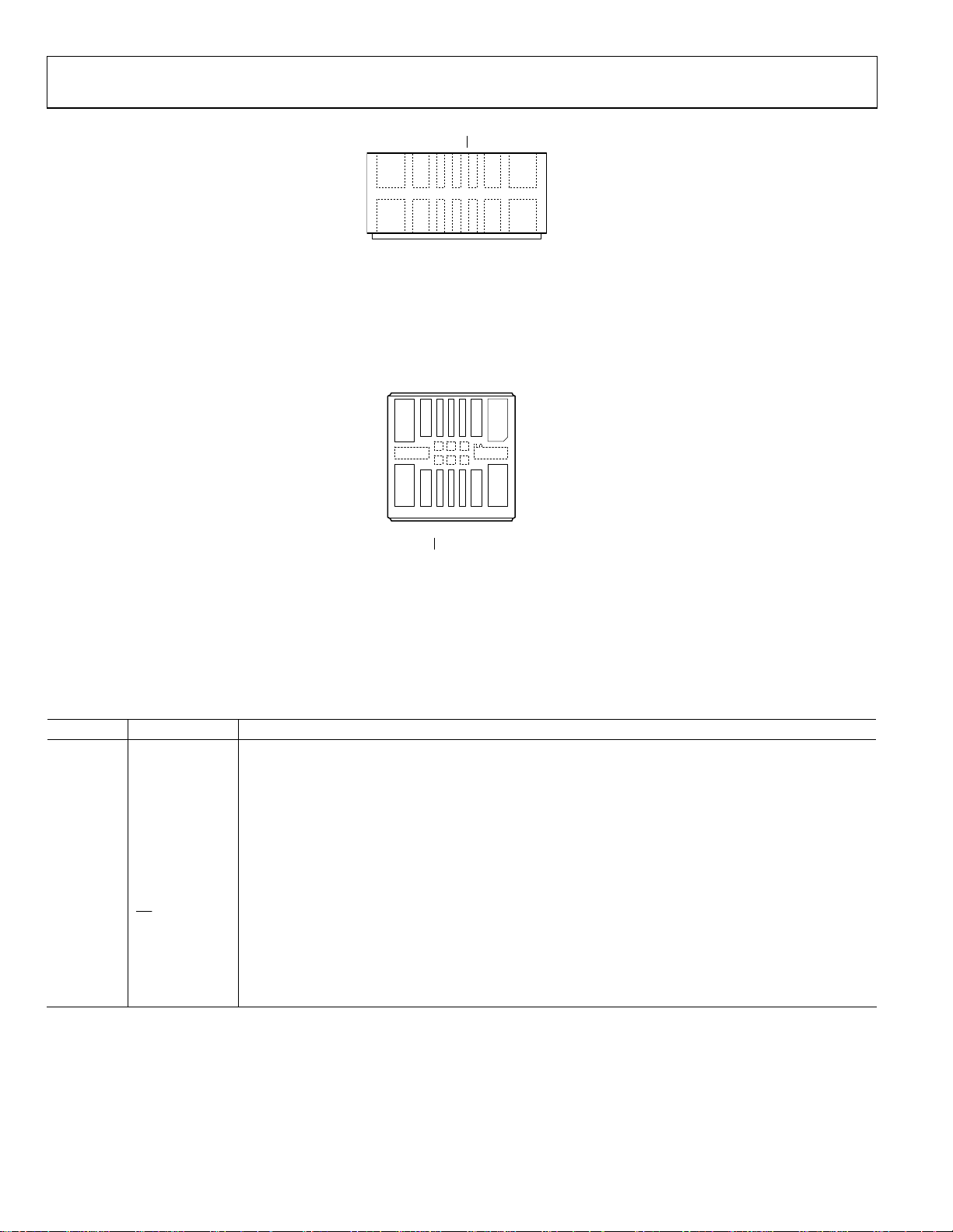
PACKAGE ORIENTATION AND LAYOUT INFORMATION
A
D
X
14
R
S
4
C
K
A
5
G
0
E
F
R
O
N
T
)
8
(P
A
1
NOTES
1. THE LCC_V PACKAGE HAS TWO TERMINALS ON TWO FACES; HOWEVER, THE TERMINALS ON THE BACK
SIDE ARE FOR INTERNAL EVALUAT ION ONL Y AND SHOULD NOT BE USED IN THE END AP PLICATION. T HE
TERMINAL S ON THE BO TTO M OF THE PACKAGE INCO RPORATE METALL IZATI ON BUMPS T HAT ENSURE A
MINIMUM SOLDER THICKNESS FOR IMPROVED SOLDER JOINT RELIABILITY. THESE BUMPS ARE NOT
PRESENT ON THE BACK SIDE TERM INALS AND, THEREFO RE, POO R SOLDER JOINT REL IABIL ITY CAN BE
ENCOUNTERED IF USED IN THE END APPLICATION. SEE THE OUTLINE DIMENSIONS SECTION FOR A
SCHEMATIC OF THE LCC_V PACKAGE.
Figure 28. 14-Terminal Ceramic LCC_V Vertical Mount
11.232
1.27
.462
0.572
1.691
Figure 29. Sample SOIC_CAV Solder Pad Layout (Land Pattern), Dimensions
Shown In Millimeters, Not To Scale
08952-022
7
08952-004
0.55
0.55
1.5
0.95
1 1
Not To Scale
1.55
2.55
5.55
2.55
Figure 30. LCC_V Solder Pad Layout, Dimensions Shown In Millimeters,
0.55
0.95
0.80.8
1.55
1.5
08952-024
Rev. B | Page 23 of 28
Page 24

ADXRS450 Data Sheet
SUPPLIER TP ≥ T
SUPPLIER
T
P
MAXIMUM RAMP-UP RATE = 3° C/sec
MAXIMUM RAMP-DOWN RATE = 6°C/sec
T
L
T
SMAX
T
SMIN
TEMPERATURE
25
PREHEAT AREA
C
t
P
t
S
TIME 25°C TO PEAK
T
C
T
–5°C
C
TIME
USER TP ≤ T
Figure 31. Recommended Soldering Profile
C
USER
t
P
t
P
t
L
TC –5°C
08952-026
Table 17. Solder Profile Conditions
Conditions
Profile Feature
Sn63/Pb37 Pb Free
Average Ramp Rate (TL to TP) 3°C/sec maximum
Preheat
Minimum Temperature (T
Maximum Temperature (T
Time (T
T
to TL
SMAX
SMIN
to T
) (tS) 60 sec to 120 sec 60 sec to 120 sec
SMAX
) 100°C 150°C
SMIN
) 150°C 200°C
SMAX
Ramp-Up Rate 3°C/sec maximum
Time Maintained above Liquidous
Liquidous Temperature (TL) 183°C 217°C
Time (tL) 60 sec to 150 sec 60 sec to 150 sec
Peak Temperature (TP) 240°C + 0°C/−5°C 260°C + 0°C/−5°C
Time Within 5°C of Actual Peak Temperature (tP) 10 sec to 30 sec 20 sec to 40 sec
Ramp-Down Rate 6°C/sec maximum
Time 25°C to Peak Temperature 6 minutes maximum 8 minutes maximum
Rev. B | Page 24 of 28
Page 25

Data Sheet ADXRS450
PACKAGE MARKING CODES
XRS450
BEYZ n
#YYWW
LLLLLLLLL
Figure 32. LCC_V and SOIC_CAV Package Marking Codes
LLLLLLLLL
Table 18. Package Code Designations
Marking Significance
XRS Angular rate sensor
450 Series number
B Temperature Grade (−40°C to +105°C)
RG Package designator (SOIC_CAV package)
EY Package designator (LCC_V package)
Z
n
#
RoHS compliant
Revision number
Pb-Free designation
YYWW Assembly date code
LLLLLLLLL Assembly lot code (up to 9 characters)
XRS450
BRGZ n
#YYWW
08952-027
Rev. B | Page 25 of 28
Page 26

ADXRS450 Data Sheet
C
V
OUTLINE DIMENSIONS
10.30 BSC
0.275
REF
7.70
7.55
7.40
INDICATOR
OPLANARITY
FRONT
9.20
9.00 SQ
8.80
0.10
3.73
3.58
3.43
0.28
0.18
0.08
PIN 1
0.50
0.45
0.40
16
1
9.59 BSC
1.27 BSC
0.75
0.70
0.65
9
8
7.80
BSC
10.42
BSC
0.25 GAGE
PLANE
8°
4°
0°
1.50
1.35
1.20
0.58
0.48
DETAIL A
0.38
Figure 33. 16-Lead Small Outline, Plastic Cavity Package [SOIC_CAV]
(RG-16-1)
Dimensions shown in millimeters
IEW
4.40
8.08
8.00
7.92
0.350
0.305
0.260
7.18
7.10
7.02
4.00
3.60
DETAIL A
BACK VI EW
0.87
0.77
0.67
072409-B
1.175
REF
C0.30
REF
1.70
REF
(ALL PINS)
1.70
REF
(ALL PINS)
1 2 345 6 7
1.00
(PINS 2, 6)
1234567
14
13 12 11 10
1.40
(PINS 1,
7, 8, 14)
(PINS 3-5, 10-12)
BOTTOM VIEW ( PADS SIDE)
0.60
(PINS 3-5)
0.30
REF
0.40
0.50
TYP
1.60
(PINS 1, 7)
8
9
0.80
(PINS 2, 6,
9, 13)
0.675 NOM
0.500 MIN
0.30
REF
0.35
REF
0.35
REF
0.80 REF
(METALLIZATION BUMP
BUMP HEIGHT 0.03 NOM)
SIDE VI EW
R0.20
REF
(PINS 2, 6)
Figure 34. 14-Terminal Ceramic Leadless Chip Carrier [LCC_V]
(EY-14-1)
Dimensions shown in millimeters
1.50
1.00
(PINS 9-10,
12-13)
8910
13 14
11 12
TERMINALS ON BACK SIDE
OF PACKAGE ARE FOR
EVALUATION TESTING ONLY.
0.80
(PINS 10,
11, 1 2)
04-08-2010-A
Rev. B | Page 26 of 28
Page 27

Data Sheet ADXRS450
ORDERING GUIDE
Temperature
Model1
ADXRS450BEYZ –40°C to +105°C 14-Terminal Ceramic Leadless Chip Carrier, Vertical Form [LCC_V] EY-14-1
ADXRS450BEYZ-RL –40°C to +105°C 14-Terminal Ceramic Leadless Chip Carrier, Vertical Form [LCC_V] EY-14-1
ADXRS450BRGZ –40°C to +105°C 16-Lead Small Outline, Plastic Cavity Package [SOIC_CAV] RG-16-1
ADXRS450BRGZ-RL –40°C to +105°C 16-Lead Small Outline, Plastic Cavity Package [SOIC_CAV] RG-16-1
EVAL-ADXRS450Z Evaluation Board SOIC_CAV
EVAL-ADXRS450Z-V Evaluation Board LCC_V
EVAL-ADXRS450Z-M
EVAL-ADXRS450Z-S
1
Z = RoHS Compliant Part.
Range Package Description
Analog Devices Inertial Sensor Evaluation System (Includes ADXRS450
Satellite)
ADXRS450 Satellite, Standalone, to be used with Inertial Sensor
Evaluation System
Package
Option
Rev. B | Page 27 of 28
Page 28

ADXRS450 Data Sheet
NOTES
©2011 Analog Devices, Inc. All rights reserved. Trademarks and
registered trademarks are the property of their respective owners.
D08952-0-12/11(B)
Rev. B | Page 28 of 28
 Loading...