

Page 1
Low Cost ⴞ2 g/ⴞ10 g Dual Axis
iMEMS
®
Accelerometers
a
FEATURES
2-Axis Acceleration Sensor on a Single IC Chip
Measures Static Acceleration as Well as Dynamic
Acceleration
Duty Cycle Output with User Adjustable Period
Low Power <0.6 mA
Faster Response than Electrolytic, Mercury or Thermal
Tilt Sensors
Bandwidth Adjustment with a Single Capacitor Per Axis
5 m
g
Resolution at 60 Hz Bandwidth
+3 V to +5.25 V Single Supply Operation
1000
g
Shock Survival
APPLICATIONS
2-Axis Tilt Sensing
Computer Peripherals
Inertial Navigation
Seismic Monitoring
Vehicle Security Systems
Battery Powered Motion Sensing
with Digital Output
ADXL202/ADXL210
GENERAL DESCRIPTION
The ADXL202/ADXL210 are low cost, low power, complete
2-axis accelerometers with a measurement range of either
±2 g/±10 g. The ADXL202/ADXL210 can measure both dy-
namic acceleration (e.g., vibration) and static acceleration (e.g.,
gravity).
The outputs are digital signals whose duty cycles (ratio of pulsewidth to period) are proportional to the acceleration in each of
the 2 sensitive axes. These outputs may be measured directly
with a microprocessor counter, requiring no A/D converter or
glue logic. The output period is adjustable from 0.5 ms to 10 ms
via a single resistor (R
voltage output proportional to acceleration is available from the
X
FILT
and Y
pins, or may be reconstructed by filtering the
FILT
duty cycle outputs.
The bandwidth of the ADXL202/ADXL210 may be set from
0.01 Hz to 5 kHz via capacitors C
floor is 500 µg/√Hz allowing signals below 5 mg to be resolved
for bandwidths below 60 Hz.
The ADXL202/ADXL210 is available in a hermetic 14-lead
Surface Mount CERPAK, specified over the 0°C to +70°C
commercial or –40°C to +85°C industrial temperature range.
). If a voltage output is desired, a
SET
and CY. The typical noise
X
C
DC
i
MEM
S
is a registered trademark of Analog Devices, Inc.
+3.0V TO +5.25V
V
DD
X SENSOR
OSCILLATOR
Y SENSOR
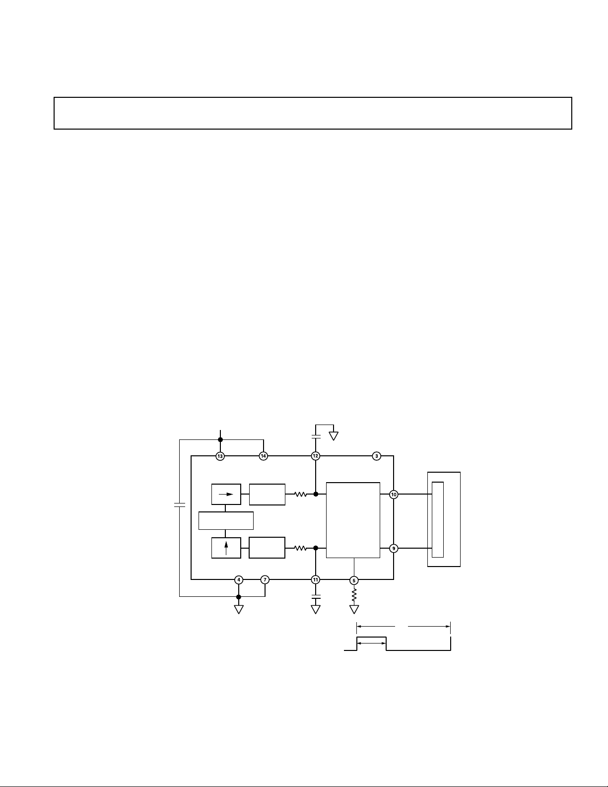
FUNCTIONAL BLOCK DIAGRAM
C
COM
V
DEMOD
DEMOD
X
X
FILT
FILT
Y
FILT
FILT
C
Y
DD
R
32kV
R
32kV
SELF TEST
ADXL202/
ADXL210
DUTY
CYCLE
MODULATOR
(DCM)
T2
R
SET
T1
A(g) = (T1/T2 – 0.5)/12.5%
0
g
= 50% DUTY CYCLE
T2 = R
/125MV
SET
T2
X OUT
Y OUT
C
O
U
mP
N
T
E
R
REV. B
Information furnished by Analog Devices is believed to be accurate and
reliable. However, no responsibility is assumed by Analog Devices for its
use, nor for any infringements of patents or other rights of third parties
which may result from its use. No license is granted by implication or
otherwise under any patent or patent rights of Analog Devices.
AIN2 =
One Technology Way, P.O. Box 9106, Norwood, MA 02062-9106, U.S.A.
Tel: 781/329-4700 World Wide Web Site: http://www.analog.com
Fax: 781/326-8703 © Analog Devices, Inc., 1999
Page 2

ADXL202/ADXL210–SPECIFICATIONS
(TA = T
R
to T
MIN
= 125 k⍀, Acceleration = 0 g, unless otherwise noted)
SET
, TA = +25ⴗC for J Grade only, VDD = +5 V,
MAX
ADXL202/JQC/AQC ADXL210/JQC/AQC
Parameter Conditions Min Typ Max Min Typ Max Units
SENSOR INPUT Each Axis
Measurement Range
Nonlinearity Best Fit Straight Line 0.2 0.2 % of FS
Alignment Error
Alignment Error X Sensor to Y Sensor ±0.01 ±0.01 Degrees
Transverse Sensitivity
1
2
3
±1.5 ±2 ±8 ±10 g
±1 ±1 Degrees
±2 ±2%
SENSITIVITY Each Axis
Duty Cycle per g T1/T2 @ +25°C 10 12.5 15 3.2 4.0 4.8 %/g
Sensitivity, Analog Output At Pins X
Temperature Drift
4
∆ from +25°C ±0.5 ±0.5 % Rdg
FILT
, Y
FILT
312 100 mV/g
ZERO g BIAS LEVEL Each Axis
0 g Duty Cycle T1/T2 25 50 75 42 50 58 %
Initial Offset ±2 ±2 g
0 g Duty Cycle vs. Supply 1.0 4.0 1.0 4.0 %/V
0 g Offset vs. Temperature
NOISE PERFORMANCE
Noise Density
5
4
∆ from +25°C 2.0 2.0 mg/°C
@ +25°C 500 1000 500 1000 µg/√Hz
FREQUENCY RESPONSE
3 dB Bandwidth Duty Cycle Output 500 500 Hz
3 dB Bandwidth At Pins X
FILT
, Y
FILT
55kHz
Sensor Resonant Frequency 10 14 kHz
FILTER
R
Tolerance 32 kΩ Nominal ±15 ±15 %
FILT
Minimum Capacitance At X
FILT
, Y
FILT
1000 1000 pF
SELF TEST
Duty Cycle Change Self-Test “0” to “1” 10 10 %
DUTY CYCLE OUTPUT STAGE
F
SET
F
Tolerance R
SET
= 125 kΩ 0.7 1.3 0.7 1.3 kHz
SET
Output High Voltage I = 25 µAV
125 MΩ/R
– 200 mV VS – 200 mV mV
S
SET
125 MΩ/R
SET
Output Low Voltage I = 25 µA 200 200 mV
T2 Drift vs. Temperature 35 35 ppm/°C
Rise/Fall Time 200 200 ns
POWER SUPPLY
Operating Voltage Range 3.0 5.25 2.7 5.25 V
Specified Performance 4.75 5.25 4.75 5.25 V
Quiescent Supply Current 0.6 1.0 0.6 1.0 mA
Turn-On Time
6
To 99% 160 C
+ 0.3 160 C
FILT
+ 0.3 ms
FILT
TEMPERATURE RANGE
Operating Range JQC 0 +70 0 +70 °C
Specified Performance AQC –40 +85 –40 +85 °C
NOTES
1
For all combinations of offset and sensitivity variation.
2
Alignment error is specified as the angle between the true and indicated axis of sensitivity.
3
Transverse sensitivity is the algebraic sum of the alignment and the inherent sensitivity errors.
4
Specification refers to the maximum change in parameter from its initial at +25 °C to its worst case value at T
5
Noise density (µg/√Hz) is the average noise at any frequency in the bandwidth of the part.
6
C
in µF. Addition of filter capacitor will increase turn on time. Please see the Application section on power cycling.
FILT
All min and max specifications are guaranteed. Typical specifications are not tested or guaranteed.
Specifications subject to change without notice.
MIN
to T
MAX
.
–2–
REV. B
Page 3
ADXL202/ADXL210
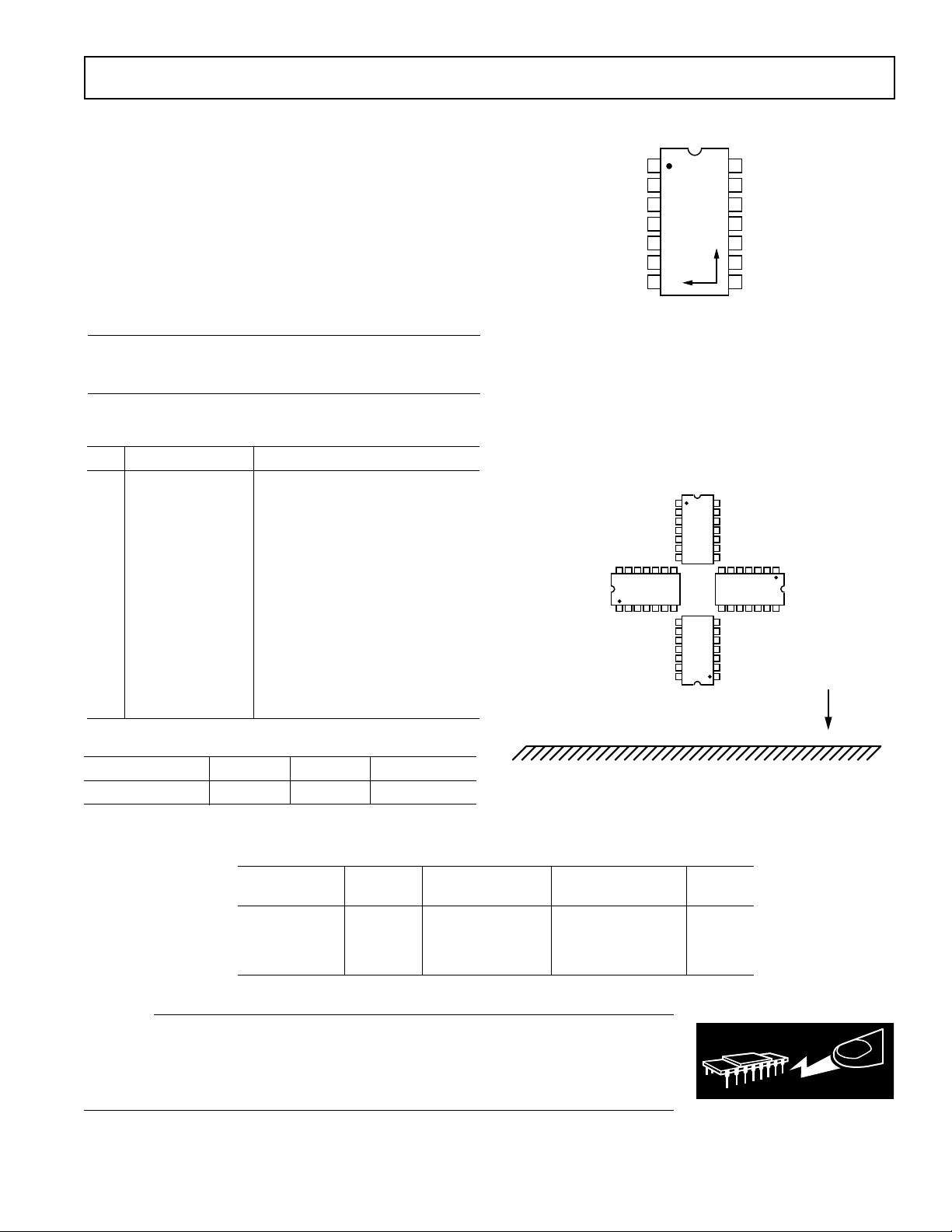
14
13
12
11
10
9
8
1
2
3
4
7
6
5
TOP VIEW
(Not to Scale)
A
Y
A
X
NC = NO CONNECT
NC
Y
FILT
X
FILT
V
DD
V
DD
V
TP
ST
COM
NC
Y
OUT
X
OUT
T2
NC
COM
ADXL202/
ADXL210
TYPICAL OUTPUT AT PIN:
9 = 50% DUTY CYCLE
10 = 62.5% DUTY CYCLE
11 = 2.5V
12 = 2.188V
TYPICAL OUTPUT AT PIN:
9 = 62.5% DUTY CYCLE
10 = 50% DUTY CYCLE
11 = 2.188V
12 = 2.5V
TYPICAL OUTPUT AT PIN:
9 = 37.5% DUTY CYCLE
10 = 50% DUTY CYCLE
11 = 2.812V
12 = 2.5V
TYPICAL OUTPUT AT PIN:
9 = 50% DUTY CYCLE
10 = 37.5% DUTY CYCLE
11 = 2.5V
12 = 2.812V
EARTH'S SURFACE
1
g
WARNING!
ESD SENSITIVE DEVICE
ABSOLUTE MAXIMUM RATINGS*
Acceleration (Any Axis, Unpowered for 0.5 ms) . . . . . . 1000 g
Acceleration (Any Axis, Powered for 0.5 ms) . . . . . . . . . 500 g
. . . . . . . . . . . . . . . . . . . . . . . . . . . . . . . . –0.3 V to +7.0 V
+V
S
Output Short Circuit Duration
(Any Pin to Common) . . . . . . . . . . . . . . . . . . . . . . Indefinite
Operating Temperature . . . . . . . . . . . . . . . . . –55°C to +125°C
Storage Temperature . . . . . . . . . . . . . . . . . . . –65°C to +150°C
*Stresses above those listed under Absolute Maximum Ratings may cause perma-
nent damage to the device. This is a stress rating only; the functional operation of
the device at these or any other conditions above those indicated in the operational
sections of this specification is not implied. Exposure to absolute maximum rating
conditions for extended periods may affect device reliability.
Drops onto hard surfaces can cause shocks of greater than 1000 g
and exceed the absolute maximum rating of the device. Care
should be exercised in handling to avoid damage.
PIN FUNCTION DESCRIPTIONS
Pin Name Description
1 NC No Connect
2V
TP
Test Point, Do Not Connect
3 ST Self Test
4 COM Common
5 T2 Connect R
to Set T2 Period
SET
6 NC No Connect
7 COM Common
8 NC No Connect
9Y
10 X
11 Y
12 X
13 V
14 V
OUT
OUT
FILT
FILT
DD
DD
Y Axis Duty Cycle Output
X Axis Duty Cycle Output
Connect Capacitor for Y Filter
Connect Capacitor for X Filter
+3 V to +5.25 V, Connect to 14
+3 V to +5.25 V, Connect to 13
PIN CONFIGURATION
Figure 1 shows the response of the ADXL202 to the Earth’s
gravitational field. The output values shown are nominal. They
are presented to show the user what type of response to expect
from each of the output pins due to changes in orientation with
respect to the Earth. The ADXL210 reacts similarly with output changes appropriate to its scale.
PACKAGE CHARACTERISTICS
Package
14-Lead CERPAK 110°C/W 30°C/W 5 Grams
CAUTION
ESD (electrostatic discharge) sensitive device. Electrostatic charges as high as 4000 V readily
accumulate on the human body and test equipment and can discharge without detection.
Although the ADXL202/ADXL210 features proprietary ESD protection circuitry, permanent
damage may occur on devices subjected to high energy electrostatic discharges. Therefore, proper
ESD precautions are recommended to avoid performance degradation or loss of functionality.
JA
JC
Device Weight
Figure 1. ADXL202/ADXL210 Nominal Response Due to
Gravity
ORDERING GUIDE
g Temperature Package Package
Model Range Range Description Option
ADXL202JQC ±20°C to +70°C 14-Lead CERPAK QC-14
ADXL202AQC ±2 –40°C to +85°C 14-Lead CERPAK QC-14
ADXL210JQC ±10 0°C to +70°C 14-Lead CERPAK QC-14
ADXL210AQC ±10 –40°C to +85°C 14-Lead CERPAK QC-14
–3–REV. B
Page 4
ADXL202/ADXL210
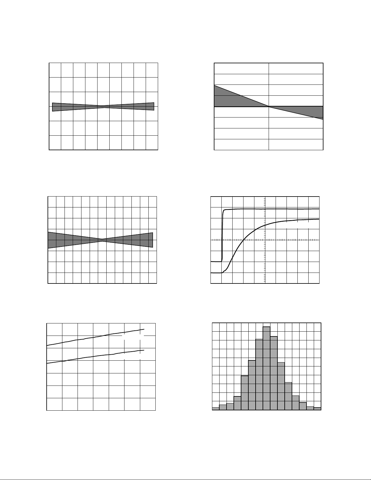
TEMPERATURE – 8C
4%
3%
–4%
–40
8525
0%
–1%
–2%
–3%
2%
1%
CHANGE IN SENSITIVITY
g
/DUTY CYCLE OUTPUT
20
6
0
–0.87g
PERCENTAGE OF SAMPLES
–0.64g –0.41g –0.17g 0.06g 0.29g 0.52g 0.75g
18
8
4
2
14
10
16
12
TYPICAL CHARACTERISTICS
1.06
1.04
1.02
1.00
0.98
0.96
PERIOD NORMALIZED TO 1 AT 25 8C
0.94
–45 90–30
–150 1530456075
TEMPERATURE – 8C
(@ +25ⴗC R
= 125 k⍀, VDD = +5 V, unless otherwise noted)
SET
Figure 2. Normalized DCM Period (T2) vs. Temperature
0.8
0.6
g
0.4
0.2
Figure 5. Typical X Axis Sensitivity Drift Due to
Temperature
3
C
= 0.01mF
2
FILT
0
OFFSET SHIFT IN
–0.2
g
–0.4
ZERO
–0.6
–0.8
–40 90–30
Figure 3. Typical Zero g Offset vs. Temperature
0.7
0.6
0.5
0.4
0.3
0.2
SUPPLY CURRENT – mA
0.1
0
–40 100–20
Figure 4. Typical Supply Current vs. Temperature
–20–100 1020304050 607080
TEMPERATURE – 8C
VS = 5 VDC
VS = 3.5 VDC
020406080
TEMPERATURE – 8C
–4–
VOLTS
1
0
0 0.4 0.8 1.2 1.4
FREQUENCY – ms
Figure 6. Typical Turn-On Time
Figure 7. Typical Zero g Distribution at +25°C
REV. B
Page 5

9
NUMBER OF AVERAGE SAMPLES
14
12
0
1644
TOTAL RMS NOISE – m
g
16
8
6
4
2
10
C
FILT
= 0.047mF
BW = 100Hz
C
FILT
= 0.1mF
BW = 50Hz
C
FILT
= 0.47mF
BW = 10Hz
C
FILT
= 0.01mF
BW = 500Hz
T2 = 1ms
DEGREES OF MISALIGNMENT
20
6
0
–1.375
0.375
% OF PARTS
–1.125
–0.875
–0.625
–0.375
–0.0125
18
8
4
2
16
12
14
10
0.625
0.875
1.125
1.375
0.0125
8
7
6
5
4
3
PERCENTAGE OF SAMPLES
2
1
0
11.5 11.7 11.9 12.2 12.4 12.6 12.8 13.1 13.3 13.5 13.7
11.3
DUTY CYCLE OUTPUT – % per
ADXL202/ADXL210
g
Figure 8. Typical Sensitivity per g at +25°C
14
12
g
10
8
6
4
TOTAL RMS NOISE – m
2
0
0.01mF
500Hz
Figure 9. Typical Noise at X
0.047mF
100Hz
CX, C
Y
BANDWIDTH
0.1mF
50Hz
FILT
Output
0.47mF
10Hz
Figure 10. Typical Noise at Digital Outputs
Figure 11. Rotational Die Alignment
–5–REV. B
Page 6

ADXL202/ADXL210
DEFINITIONS
T1 Length of the “on” portion of the cycle.
T2 Length of the total cycle.
Duty Cycle Ratio of the “on” time (T1) of the cycle to the total
cycle (T2). Defined as T1/T2 for the ADXL202/
ADXL210.
Pulsewidth Time period of the “on” pulse. Defined as T1 for
the ADXL202/ADXL210.
THEORY OF OPERATION
The ADXL202/ADXL210 are complete dual axis acceleration
measurement systems on a single monolithic IC. They contain a
polysilicon surface-micromachined sensor and signal conditioning circuitry to implement an open loop acceleration measurement architecture. For each axis, an output circuit converts the
analog signal to a duty cycle modulated (DCM) digital signal
that can be decoded with a counter/timer port on a microprocessor. The ADXL202/ADXL210 are capable of measuring
both positive and negative accelerations to a maximum level of
±2 g or ±10 g. The accelerometer measures static acceleration
forces such as gravity, allowing it to be used as a tilt sensor.
The sensor is a surface micromachined polysilicon structure
built on top of the silicon wafer. Polysilicon springs suspend the
structure over the surface of the wafer and provide a resistance
against acceleration forces. Deflection of the structure is measured using a differential capacitor that consists of independent
fixed plates and central plates attached to the moving mass. The
fixed plates are driven by 180° out of phase square waves. An
acceleration will deflect the beam and unbalance the differential
capacitor, resulting in an output square wave whose amplitude
is proportional to acceleration. Phase sensitive demodulation
techniques are then used to rectify the signal and determine the
direction of the acceleration.
The output of the demodulator drives a duty cycle modulator
(DCM) stage through a 32 kΩ resistor. At this point a pin is
available on each channel to allow the user to set the signal
bandwidth of the device by adding a capacitor. This filtering
improves measurement resolution and helps prevent aliasing.
After being low-pass filtered, the analog signal is converted to a
duty cycle modulated signal by the DCM stage. A single resistor
sets the period for a complete cycle (T2), which can be set between 0.5 ms and 10 ms (see Figure 12). A 0 g acceleration
produces a nominally 50% duty cycle. The acceleration signal
can be determined by measuring the length of the T1 and T2
pulses with a counter/timer or with a polling loop using a low
cost microcontroller.
An analog output voltage can be obtained either by buffering the
signal from the X
FILT
and Y
pin, or by passing the duty cycle
FILT
signal through an RC filter to reconstruct the dc value.
The ADXL202/ADXL210 will operate with supply voltages as
low as 3.0 V or as high as 5.25 V.
T2
T1
A(g) = (T1/T2 – 0.5)/12.5%
0
g
= 50% DUTY CYCLE
T2(s) = R
(V)/125MV
SET
Figure 12. Typical Output Duty Cycle
APPLICATIONS
POWER SUPPLY DECOUPLING
For most applications a single 0.1 µF capacitor, C
, will ad-
DC
equately decouple the accelerometer from signal and noise on
the power supply. However, in some cases, especially where digital
devices such as microcontrollers share the same power supply, digital noise on the supply may cause interference on the ADXL202/
ADXL210 output. This is often observed as a slowly undulating
fluctuation of voltage at X
FILT
and Y
. If additional decou-
FILT
pling is needed, a 100 Ω (or smaller) resistor or ferrite beads,
may be inserted in the ADXL202/ADXL210’s supply line.
DESIGN PROCEDURE FOR THE ADXL202/ADXL210
The design procedure for using the ADXL202/ADXL210 with a
duty cycle output involves selecting a duty cycle period and a
filter capacitor. A proper design will take into account the application requirements for bandwidth, signal resolution and acquisition time, as discussed in the following sections.
V
DD
The ADXL202/ADXL210 have two power supply (VDD) Pins:
13 and 14. These two pins should be connected directly together.
COM
The ADXL202/ADXL210 have two commons, Pins 4 and 7.
These two pins should be connected directly together and Pin 7
grounded.
V
TP
This pin is to be left open; make no connections of any kind to
this pin.
Decoupling Capacitor C
A 0.1 µF capacitor is recommended from V
DC
to COM for
DD
power supply decoupling.
ST
The ST pin controls the self-test feature. When this pin is set to
, an electrostatic force is exerted on the beam of the acceler-
V
DD
ometer. The resulting movement of the beam allows the user to
test if the accelerometer is functional. The typical change in
output will be 10% at the duty cycle outputs (corresponding to
800 mg). This pin may be left open circuit or connected to
common in normal use.
Duty Cycle Decoding
The ADXL202/ADXL210’s digital output is a duty cycle modulator. Acceleration is proportional to the ratio T1/T2. The
nominal output of the ADXL202 is:
0 g = 50% Duty Cycle
Scale factor is 12.5% Duty Cycle Change per g
The nominal output of the ADXL210 is:
0 g = 50% Duty Cycle
Scale factor is 4% Duty Cycle Change per g
These nominal values are affected by the initial tolerance of the
device including zero g offset error and sensitivity error.
T2 does not have to be measured for every measurement cycle.
It need only be updated to account for changes due to temperature, (a relatively slow process). Since the T2 time period is
shared by both X and Y channels, it is necessary only to measure it on one channel of the ADXL202/ADXL210. Decoding
algorithms for various microcontrollers have been developed.
Consult the appropriate Application Note.
–6–
REV. B
Page 7

C
DC
+3.0V TO +5.25V
V
DD
X SENSOR
OSCILLATOR
Y SENSOR
V
DEMOD
DEMOD
ADXL202/ADXL210
C
X
R
FILT
32kV
R
FILT
32kV
X
DD
FILT
ADXL202/
ADXL210
DUTY
CYCLE
MODULATOR
(DCM)
SELF TEST
X OUT
Y OUT
T2
C
O
U
mP
N
T
E
R
T1
A(g) = (T1/T2 – 0.5)/12.5%
0g = 50% DUTY CYCLE
T2 = R
/125MV
SET
COM
Y
FILT
T2
R
C
Y
SET
Figure 13. Block Diagram
Setting the Bandwidth Using CX and C
Y
The ADXL202/ADXL210 have provisions for bandlimiting the
X
FILT
and Y
pins. Capacitors must be added at these pins to
FILT
implement low-pass filtering for antialiasing and noise reduction. The equation for the 3 dB bandwidth is:
F
=
or, more simply,
–3 dB
F
–3 dB
π
2
()
5 µF
=
C
(X ,Y )
The tolerance of the internal resistor (R
1
(32 kΩ) ×C(x , y )
), can vary as much
FILT
as ±25% of its nominal value of 32 kΩ; so the bandwidth will
vary accordingly. A minimum capacitance of 1000 pF for C
(X, Y)
is required in all cases.
Table I. Filter Capacitor Selection, CX and C
Y
Capacitor
Bandwidth Value
10 Hz 0.47 µF
50 Hz 0.10 µF
100 Hz 0.05 µF
200 Hz 0.027 µF
500 Hz 0.01 µF
5 kHz 0.001 µF
Setting the DCM Period with R
SET
The period of the DCM output is set for both channels by a
single resistor from R
to ground. The equation for the period
SET
is:
R
(Ω)
SET
T 2 =
125 MΩ
A 125 kΩ resistor will set the duty cycle repetition rate to ap-
proximately 1 kHz, or 1 ms. The device is designed to operate at
duty cycle periods between 0.5 ms and 10 ms.
Table II. Resistor Values to Set T2
T2 R
SET
1 ms 125 kΩ
2 ms 250 kΩ
5 ms 625 kΩ
10 ms 1.25 MΩ
Note that the R
analog output is desired. Use an R
and 2 MΩ when taking the output from X
resistor should be place close to the T2 Pin to minimize
R
SET
should always be included, even if only an
SET
value between 500 kΩ
SET
FILT
or Y
FILT
. The
parasitic capacitance at this node.
Selecting the Right Accelerometer
For most tilt sensing applications the ADXL202 is the most
appropriate accelerometer. Its higher sensitivity (12.5%/g allows
the user to use a lower speed counter for PWM decoding while
maintaining high resolution. The ADXL210 should be used in
applications where accelerations of greater than ±2 g are expected.
MICROCOMPUTER INTERFACES
The ADXL202/ADXL210 were specifically designed to work
with low cost microcontrollers. Specific code sets, reference
designs, and application notes are available from the factory.
This section will outline a general design procedure and discuss
the various trade-offs that need to be considered.
The designer should have some idea of the required performance of the system in terms of:
Resolution: the smallest signal change that needs to be detected.
Bandwidth: the highest frequency that needs to be detected.
Acquisition Time: the time that will be available to acquire the
signal on each axis.
These requirements will help to determine the accelerometer
bandwidth, the speed of the microcontroller clock and the
length of the T2 period.
When selecting a microcontroller it is helpful to have a counter
timer port available. The microcontroller should have provisions
for software calibration. While the ADXL202/ADXL210 are
highly accurate accelerometers, they have a wide tolerance for
–7–REV. B
Page 8

ADXL202/ADXL210
initial offset. The easiest way to null this offset is with a calibration factor saved on the microcontroller or by a user calibration
for zero g. In the case where the offset is calibrated during manufacture, there are several options, including external EEPROM
and microcontrollers with “one-time programmable” features.
DESIGN TRADE-OFFS FOR SELECTING FILTER
CHARACTERISTICS: THE NOISE/BW TRADE-OFF
The accelerometer bandwidth selected will determine the measurement resolution (smallest detectable acceleration). Filtering
can be used to lower the noise floor and improve the resolution
of the accelerometer. Resolution is dependent on both the analog filter bandwidth at X
FILT
and Y
and on the speed of the
FILT
microcontroller counter.
The analog output of the ADXL202/ADXL210 has a typical
bandwidth of 5 kHz, much higher than the duty cycle stage is
capable of converting. The user must filter the signal at this
point to limit aliasing errors. To minimize DCM errors the
analog bandwidth should be less than 1/10 the DCM frequency.
Analog bandwidth may be increased to up to 1/2 the DCM
frequency in many applications. This will result in greater dynamic error generated at the DCM.
The analog bandwidth may be further decreased to reduce noise
and improve resolution. The ADXL202/ADXL210 noise has
the characteristics of white Gaussian noise that contributes
equally at all frequencies and is described in terms of µg per root
Hz; i.e., the noise is proportional to the square root of the bandwidth of the accelerometer. It is recommended that the user limit
bandwidth to the lowest frequency needed by the application, to
maximize the resolution and dynamic range of the accelerometer.
With the single pole roll-off characteristic, the typical noise of
the ADXL202/ADXL210 is determined by the following equation:
Noise rms
()
= 500 µg/ Hz
× BW ×1. 5
At 100 Hz the noise will be:
Noise rms
()
= 500 µg/ Hz
× 100 × (1. 5 )
=6.12 mg
Often the peak value of the noise is desired. Peak-to-peak noise
can only be estimated by statistical methods. Table III is useful
for estimating the probabilities of exceeding various peak values,
given the rms value.
Table III. Estimation of Peak-to-Peak Noise
% of Time that Noise
Nominal Peak-to-Peak Will Exceed Nominal
Value Peak-to-Peak Value
2.0 × rms 32%
4.0 × rms 4.6%
6.0 × rms 0.27%
8.0 × rms 0.006%
Table IV gives typical noise output of the ADXL202/ADXL210
for various C
and CY values.
X
Table IV. Filter Capacitor Selection, CX and C
Y
Peak-to-Peak Noise
Estimate 95%
Bandwidth CX, CYrms Noise Probability (rms ⴛ 4)
10 Hz 0.47 µF 1.9 mg 7.6 mg
50 Hz 0.10 µF 4.3 mg 17.2 mg
100 Hz 0.05 µF 6.1 mg 24.4 mg
200 Hz 0.027 µF 8.7 mg 35.8 mg
500 Hz 0.01 µF 13.7 mg 54.8 mg
CHOOSING T2 AND COUNTER FREQUENCY: DESIGN
TRADE-OFFS
The noise level is one determinant of accelerometer resolution.
The second relates to the measurement resolution of the
counter when decoding the duty cycle output.
The ADXL202/ADXL210’s duty cycle converter has a resolution of approximately 14 bits; better resolution than the accelerometer itself. The actual resolution of the acceleration signal is,
however, limited by the time resolution of the counting devices
used to decode the duty cycle. The faster the counter clock, the
higher the resolution of the duty cycle and the shorter the T2
period can be for a given resolution. The following table shows
some of the trade-offs. It is important to note that this is the
resolution due to the microprocessors’s counter. It is probable
that the accelerometer’s noise floor may set the lower limit on
the resolution, as discussed in the previous section.
Table V. Trade-Offs Between Microcontroller Counter Rate,
T2 Period and Resolution of Duty Cycle Modulator
ADXL202/ CounterADXL210 Clock Counts
Sample Rate per T2 Counts Resolution
R
T2 (ms) (k⍀) Rate (MHz) Cycle per g (mg)
1.0 124 1000 2.0 2000 250 4.0
1.0 124 1000 1.0 1000 125 8.0
1.0 124 1000 0.5 500 62.5 16.0
5.0 625 200 2.0 10000 1250 0.8
5.0 625 200 1.0 5000 625 1.6
5.0 625 200 0.5 2500 312.5 3.2
10.0 1250 100 2.0 20000 2500 0.4
10.0 1250 100 1.0 10000 1250 0.8
10.0 1250 100 0.5 5000 625 1.6
SET
The peak-to-peak noise value will give the best estimate of the
uncertainty in a single measurement.
–8–
REV. B
Page 9

ADXL202/ADXL210
Y
X
3608 OF TILT
1
g
STRATEGIES FOR USING THE DUTY CYCLE OUTPUT
WITH MICROCONTROLLERS
Application notes outlining various strategies for using the duty
cycle output with low cost microcontrollers are available from
the factory.
USING THE ADXL202/ADXL210 AS A DUAL AXIS TILT
SENSOR
One of the most popular applications of the ADXL202/ADXL210
is tilt measurement. An accelerometer uses the force of gravity
as an input vector to determine orientation of an object in space.
An accelerometer is most sensitive to tilt when its sensitive axis
is perpendicular to the force of gravity, i.e., parallel to the
earth’s surface. At this orientation its sensitivity to changes in
tilt is highest. When the accelerometer is oriented on axis to
gravity, i.e., near its +1 g or –1 g reading, the change in output
acceleration per degree of tilt is negligible. When the accelerometer is perpendicular to gravity, its output will change nearly
17.5 mg per degree of tilt, but at 45° degrees it is changing only
at 12.2 mg per degree and resolution declines. The following
table illustrates the changes in the X and Y axes as the device is
tilted ±90° through gravity.
+908
Y
X
08
1
g
A DUAL AXIS TILT SENSOR: CONVERTING
ACCELERATION TO TILT
When the accelerometer is oriented so both its X and Y axes are
parallel to the earth’s surface it can be used as a two axis tilt
sensor with a roll and a pitch axis. Once the output signal from
the accelerometer has been converted to an acceleration that
varies between –1 g and +1 g, the output tilt in degrees is calculated as follows:
Pitch = ASIN (Ax/1 g)
Roll = ASIN (Ay/1 g)
Be sure to account for overranges. It is possible for the acceler-
ometers to output a signal greater than ±1 g due to vibration,
shock or other accelerations.
MEASURING 360ⴗ OF TILT
It is possible to measure a full 360° of orientation through grav-
ity by using two accelerometers oriented perpendicular to one
another (see Figure 15). When one sensor is reading a maximum change in output per degree, the other is at its minimum.
–908
X OUTPUT Y OUTPUT (g)
X AXIS ⌬ PER ⌬ PER
ORIENTATION DEGREE OF DEGREE OF
TO HORIZON (ⴗ) X OUTPUT (g) TILT (mg) Y OUTPUT (g) TILT (mg)
–90 –1.000 –0.2 0.000 17.5
–75 –0.966 4. 4 0.259 16.9
–60 –0.866 8. 6 0.500 15.2
–45 –0.707 12.2 0.707 12.4
–30 –0.500 15.0 0.866 8.9
–15 –0.259 16.8 0.966 4.7
– 0 0.000 17.5 1.000 0.2
– 15 0.259 16.9 0.966 –4.4
– 30 0.500 15.2 0.866 –8.6
– 45 0.707 12.4 0.707 –12.2
– 60 0.866 8.9 0.500 –15.0
– 75 0.966 4.7 0.259 –16.8
– 90 1.000 0.2 0.000 –17.5
Figure 14. How the X and Y Axes Respond to Changes in
Tilt
Figure 15. Using a Two-Axis Accelerometer to Measure
360
°
of Tilt
–9–REV. B
Page 10

ADXL202/ADXL210
USING THE ANALOG OUTPUT
The ADXL202/ADXL210 was specifically designed for use with
its digital outputs, but has provisions to provide analog outputs
as well.
Duty Cycle Filtering
An analog output can be reconstructed by filtering the duty
cycle output. This technique requires only passive components.
The duty cycle period (T2) should be set to 1 ms. An RC filter
with a 3 dB point at least a factor of 10 less than the duty cycle
frequency is connected to the duty cycle output. The filter resis-
tor should be no less than 100 kΩ to prevent loading of the
output stage. The analog output signal will be ratiometric to the
supply voltage. The advantage of this method is an output scale
factor of approximately double the analog output. Its disadvantage is that the frequency response will be lower than when
, Y
using the X
X
, Y
FILT
FILT
FILT
Output
FILT
output.
The second method is to use the analog output present at the
and Y
X
FILT
pin. Unfortunately, these pins have a 32 kΩ
FILT
output impedance and are not designed to drive a load directly.
An op amp follower may be required to buffer this pin. The
advantage of this method is that the full 5 kHz bandwidth of the
accelerometer is available to the user. A capacitor still must be
added at this point for filtering. The duty cycle converter should
be kept running by using R
<10 MΩ. Note that the acceler-
SET
ometer offset and sensitivity are ratiometric to the supply voltage. The offset and sensitivity are nominally:
0 g Offset = V
ADXL202 Sensitivity = (60 mV × V
ADXL210 Sensitivity = (20 mV × V
USING THE ADXL202/ADXL210 IN VERY LOW POWER
APPLICATIONS
/2 2.5 V at +5 V
DD
)/g 300 mV/g at +5 V, V
S
)/g 100 mV/g at +5 V, V
S
DD
DD
An application note outlining low power strategies for the
ADXL202/ADXL210 is available. Some key points are presented here. It is possible to reduce the ADXL202/ADXL210’s
average current from 0.6 mA to less than 20 µA by using the
following techniques:
1. Power Cycle the accelerometer.
2. Run the accelerometer at a Lower Voltage, (Down to 3 V).
Power Cycling with an External A/D
Depending on the value of the X
capacitor, the ADXL202/
FILT
ADXL210 is capable of turning on and giving a good reading in
1.6 ms. Most microcontroller based A/Ds can acquire a reading
in another 25 µs. Thus it is possible to turn on the ADXL202/
ADXL210 and take a reading in <2 ms. If we assume that a
20 Hz sample rate is sufficient, the total current required to
take 20 samples is 2 ms × 20 samples/s × 0.6 mA = 24 µA aver-
age current. Running the part at 3 V will reduce the supply
current from 0.6 mA to 0.4 mA, bringing the average current
down to 16 µA.
The A/D should read the analog output of the ADXL202/
ADXL210 at the X
FILT
and Y
pins. A buffer amplifier is
FILT
recommended, and may be required in any case to amplify the
analog output to give enough resolution with an 8-bit to 10-bit
converter.
Power Cycling When Using the Digital Output
An alternative is to run the microcontroller at a higher clock
rate and put it into shutdown between readings, allowing the
use of the digital output. In this approach the ADXL202/
ADXL210 should be set at its fastest sample rate (T2 = 0.5 ms),
with a 500 Hz filter at X
FILT
and Y
. The concept is to ac-
FILT
quire a reading as quickly as possible and then shut down the
ADXL202/ADXL210 and the microcontroller until the next
sample is needed.
In either of the above approaches, the ADXL202/ADXL210
can be turned on and off directly using a digital port pin on the
microcontroller to power the accelerometer without additional
components. The port should be used to switch the common
pin of the accelerometer so the port pin is “pulling down.”
CALIBRATING THE ADXL202/ADXL210
The initial value of the offset and scale factor for the ADXL202/
ADXL210 will require calibration for applications such as tilt
measurement. The ADXL202/ADXL210 architecture has been
designed so that these calibrations take place in the software of
the microcontroller used to decode the duty cycle signal. Calibration factors can be stored in EEPROM or determined at
turn-on and saved in dynamic memory.
For low g applications, the force of gravity is the most stable,
accurate and convenient acceleration reference available. A
reading of the 0 g point can be determined by orientating the
device parallel to the earth’s surface and then reading the output.
A more accurate calibration method is to make a measurements
at +1 g and –1 g. The sensitivity can be determined by the two
measurements.
To calibrate, the accelerometer’s measurement axis is pointed
directly at the earth. The 1 g reading is saved and the sensor is
turned 180° to measure –1 g. Using the two readings, the sensi-
tivity is:
Let A = Accelerometer output with axis oriented to +1 g
Let B = Accelerometer output with axis oriented to –1 g then:
Sensitivity = [A – B]/2 g
For example, if the +1 g reading (A) is 55% duty cycle and the
–1 g reading (B) is 32% duty cycle, then:
Sensitivity = [55% – 32%]/2 g = 11.5%/g
These equations apply whether the output is analog, or duty
cycle.
Application notes outlining algorithms for calculating acceleration from duty cycle and automated calibration routines are
available from the factory.
–10–
REV. B
Page 11

OUTLINE DIMENSIONS
Dimensions shown in inches and (mm).
14-Lead CERPAK
(QC-14)
0.390 (9.906)
MAX
ADXL202/ADXL210
0.291 (7.391)
0.285 (7.239)
PIN 1
0.020 (0.508)
0.004 (0.102)
SEATING
PLANE
14
1
0.050
(1.27)
BSC
0.300 (7.62)
0.020 (0.508)
0.013 (0.330)
8
0.419 (10.643)
0.394 (10.008)
7
0.195 (4.953)
0.115 (2.921)
0.215 (5.461)
0.119 (3.023)
0.0125 (0.318)
0.009 (0.229)
0.345 (8.763)
0.290 (7.366)
0.050 (1.270)
0.016 (0.406)
C3037b–2–4/99
8°
0°
PRINTED IN U.S.A.
–11–REV. B
 Loading...