

Page 1
61 g to 65 g Single Chip Accelerometer
a
FEATURES
g
5 milliNoise Level 123 Less than the ADXL50
User Selectable Full Scale from 61 g to 65
Output Scale Selectable from 200 mV/g to 1 V/
Complete Acceleration Measurement System on a
Self Test on Digital Command
+5 V Single Supply Operation
1000
APPLICATIONS
Low Cost Sensor for Vibration Measurement
Tilt Sensing with Faster Response than Electrolytic or
More Sensitive Alarms and Motion Detectors
Affordable Inertial Sensing of Velocity and Position
GENERAL DESCRIPTION
The ADXL05 is a complete acceleration measurement system
on a single monolithic IC. The ADXL05 will measure accelerations with full-scale ranges of ±5 g to ±1 g or less. Typical noise
Resolution
Single Chip IC
g
Shock Survival
Mercury Sensors
g
g
with Signal Conditioning
ADXL05*
floor is 500 µg/√Hz, (12× less than the ADXL50), allowing signals below 5 milli-g to be resolved. The ADXL05 is a force balanced capacitive accelerometer with the capability to measure
both ac accelerations (typical of vibration) or dc accelerations
(such as inertial force or gravity). Three external capacitors and
a +5 volt regulated power supply are all that is required to
measure accelerations up to ±5 g. Three resistors are used to
configure the output buffer amplifier to set scale factors from
200 mV/g to 1 V/g. External capacitors may be added to the
resistor network to provide 1 or 2 poles of filtering. No additional active components are required to interface directly to
most analog to digital converters (ADCs).
The device features a TTL compatible self-test function that
can electrostatically deflect the sensor beam at any time to verify
that the sensor and its electronics are functioning correctly.
The ADXL05 is available in a hermetic 10-pin TO-100 metal
can, specified over the 0°C to +70°C commercial, and –40°C to
+85°C industrial temperature ranges. Contact factory for availability of automotive grade devices.
OSCILLATOR
DECOUPLING
CAPACITOR
C2
SELF-TEST
(ST)
*Patents pending.
4
7
COM
ADXL05
OSCILLATOR
C3
+5V
15
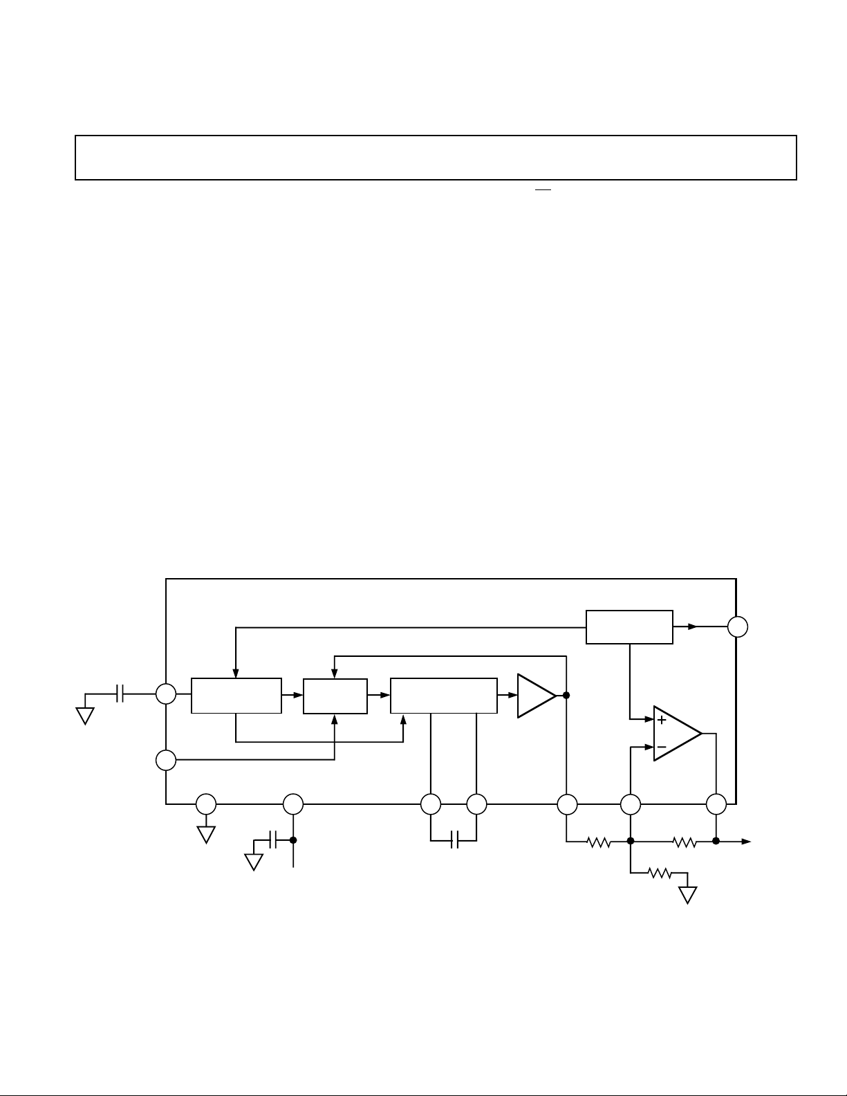
FUNCTIONAL BLOCK DIAGRAM
SENSOR
DEMODULATOR
C1
DEMODULATOR
CAPACITOR
32
C1
PREAMP
V
PR
8
REFERENCE
10
R1
+1.8V
V
IN–
BUFFER
AMP
R3
R2
+3.4V
V
REF
6
OUTPUT
9
V
OUT
REV. B
Information furnished by Analog Devices is believed to be accurate and
reliable. However, no responsibility is assumed by Analog Devices for its
use, nor for any infringements of patents or other rights of third parties
which may result from its use. No license is granted by implication or
otherwise under any patent or patent rights of Analog Devices.
© Analog Devices, Inc., 1996
One Technology Way, P.O. Box 9106, Norwood. MA 02062-9106, U.S.A.
Tel: 617/329-4700 Fax: 617/326-8703
Page 2

ADXL05–SPECIFICA TIONS
(TA = T
MIN
to T
, TA = +258C for J Grade Only, VS = +5 V, @ Acceleration = 0 g,
MAX
unless otherwise noted)
Parameter Conditions Min Typ Max Units
ADXL05J/A
SENSOR INPUT
Measurement Range Guaranteed Full Scale –5 +5 g
Nonlinearity Best Fit Straight Line, 5 g FS 0.2 % of FS
Alignment Error
Transverse Sensitivity
1
2
± 1 Degrees
± 2%
SENSITIVITY
Initial Sensitivity at V
Initial Sensitivity at V
Temperature Drift
PR
OUT
3
ZERO g BIAS LEVEL at V
Initial Offset 1.50 1.80 2.10 V
vs. Temperature
3
+25°C 175 200 225 mV/g
+25°C, R3/R1 = 5 0.875 1.000 1.125 V/g
± 0.5 % of Reading
PR
± 25/40 mV
vs. Supply VS = 4.75 V to 5.25 V 10 32 mV/V
NOISE PERFORMANCE at V
PR
Voltage Noise Density BW = 4 Hz to 1 kHz 500 1000 µg/√Hz
Noise in 100 Hz Bandwidth 5mg rms
Noise in 10 Hz Bandwidth 1.6 mg rms
FREQUENCY RESPONSE
3 dB Bandwidth
3 dB Bandwidth
4
4
C1 = 0.022 µF (See Figure 9) 1000 1600 Hz
C1 = 0.010 µF 4 kHz
Sensor Resonant Frequency 12 kHz
SELF TEST INPUT
Output Change at V
5
PR
ST Pin from Logic “0” to “1” –0.85 –1.00 –1.15 V
Logic “1” Voltage 2.0 V
Logic “0” Voltage 0.8 V
Input Resistance To Common 50 kΩ
+3.4 V REFERENCE
Output Voltage 3.350 3.400 3.450 V
Output Temperature Drift
3
±5mV
Power Supply Rejection DC, VS = +4.75 V to +5.25 V 1 10 mV/V
Output Current Sourcing 500 µA
PREAMPLIFIER OUTPUT
Voltage Swing 0.25 VS – 1.4 V
Current Output Source or Sink 30 80 µA
Capacitive Load Drive 100 pF
BUFFER AMPLIFIER
Input Offset Voltage
6
Delta from Nominal 1.800 V ±10 ±25 mV
Input Bias Current 520nA
Open-Loop Gain DC 80 dB
Unity Gain Bandwidth 200 kHz
Output Voltage Swing I
= ±100 µA 0.25 VS – 0.25 V
OUT
Capacitive Load Drive 1000 pF
Power Supply Rejection DC, VS = +4.75 V to +5.25 V 1 10 mV/V
POWER SUPPLY
Operating Voltage Range 4.75 5.25 V
Quiescent Supply Current 8.0 10.0 mA
TEMPERATURE RANGE
Operating Range J 0 +70 °C
Specified Performance A –40 +85 °C
Automotive Grade* –40 +125 °C
NOTES
1
Alignment error is specified as the angle between the true and indicated axis of sensitivity, (see Figure 2).
2
Transverse sensitivity is measured with an applied acceleration that is 90° from the indicated axis of sensitivity. Transverse sensitivity is specified as the percent of
transverse acceleration that appears at the V
3
Specification refers to the maximum change in parameter from its initial at +25°C to its worst case value at T
4
Frequency at which response is 3 dB down from dc response assuming an exact C1 value is used. Maximum recommended BW is 6 kHz using a 0.010 µF capacitor, refer to
Figure 9.
5
Applying logic high to the self-test input has the effect of applying an acceleration of –5 g to the ADXL05.
6
Input offset voltage is defined as the output voltage differential from 1.800 V when the amplifier is connected as a follower. The voltage at this pin has a temperature drift
proportional to that of the 3.4 V reference.
*Contact factory for availability of automotive grade devices.
All min and max specifications are guaranteed. Typical specifications are not tested or guaranteed.
Specifications subject to change without notice.
output. This is the algebraic sum of the alignment and the inherent sensor sensitivity errors, (see Figure 2).
PR
MIN
to T
MAX
.
–2–
REV. B
Page 3
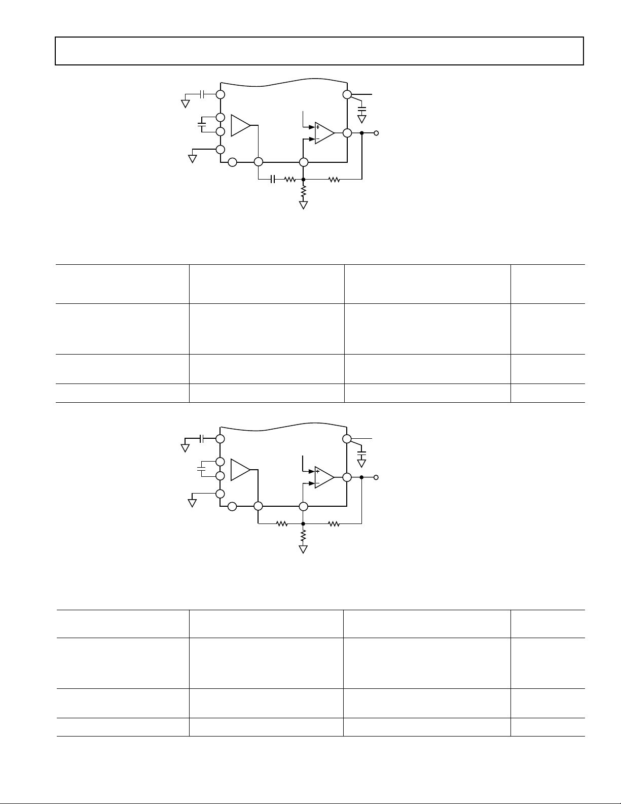
System Performance Specifications–ADXL05
0.022µF
0.022µF
COM
C2
4
ADXL05
C1
C1
2
3
5
+3.4V
REF
6
PRE-AMP
8
V
PR
C4
1.8V
10
V
R1
IN–
R2
BUFFER
AMP
R3
1
+5V
C3
0.1µF
9
V
OUT
NOMINAL VALUES:
R1 = 49.9kΩ
R3 = 249kΩ
R2 = 640kΩ
AC COUPLED CONNECTION (61.5 g Full Scale)
(@ V
Terminal (Pin 9), unless otherwise noted. 0 g Bias Level = +2.5 V, C1 = 0.022 mF, R2 = 2.57 R3
OUT
ADXL05J/A
Parameter Conditions Min Typ Max Units
Buffer Gain G = R3/R1* 5
FULL-SCALE RANGE –1.5 +1.5 g
SENSITIVITY @
Temperature Drift T
ZERO g BIAS LEVEL @ +25°C 2.5 V
Temperature Drift +25°C to T
FREQUENCY RESPONSE C4 = 3.3 µF, R1 = 49.9 kΩ 1 1000 Hz
*Note: Resistor tolerance will affect system accuracy. Use of ±1% (or better) metal film resistors is recommended.
+25°C 875 1000 1,125 mV/g
MIN
to T
MAX
MIN
or T
MAX
±0.5 % of Reading
2/5 mV
0.022µF
0.022µF
COM
C2
4
ADXL05
C1
C1
2
3
5
+3.4V
REF
6
PRE-AMP
8
V
PR
1.8V
10
V
R1
IN–
R2
BUFFER
AMP
R3
1
+5V
C3
0.1µF
9
V
OUT
NOMINAL VALUES:
R1 = 49.9kΩ
R3 = 100kΩ (G=2)
R2 = 255kΩ (G=2)
DC COUPLED CONNECTION (62 g Full Scale)
(@ V
Terminal (Pin 9), unless otherwise noted. 0 g Bias Level = +2.5 V, C1 = 0.022 mF, R2 = 2.57 R3)
OUT
ADXL05J/A
Parameter Conditions Min Typ Max Units
Buffer Gain G = R3/R1* 2
FULL-SCALE RANGE –2 +2 g
SENSITIVITY @
Temperature Drift T
ZERO g BIAS LEVEL @ +25°C 1.75 2.5 3.2 V
Temperature Drift +25°C to T
FREQUENCY RESPONSE dc 1000 Hz
*Note: Resistor tolerance will affect system accuracy. Use of ±1% (or better) metal film resistors is recommended.
+25°C 350 400 450 mV/g
MIN
to T
MAX
MIN
or T
MAX
±0.5 % of Reading
±50/80 mV
REV. B
–3–
Page 4
ADXL05
WARNING!
ESD SENSITIVE DEVICE
ABSOLUTE MAXIMUM RATINGS*
Acceleration (Any Axis, Unpowered for 0.5 ms) . . . . . . 1000 g
Acceleration (Any Axis, Powered for 0.5 ms) . . . . . . . . . . 500 g
+V
. . . . . . . . . . . . . . . . . . . . . . . . . . . . . . . . –0.3 V to +7.0 V
S
Package Characteristics
Package u
JA
10-Pin TO-100 130°C/W 30°C/W 5 Grams
Output Short Circuit Duration
(V
, V
, V
PR
OUT
Operating Temperature . . . . . . . . . . . . . . . . .–55°C to +125°C
Storage Temperature . . . . . . . . . . . . . . . . . . .–65°C to +150°C
*Stresses above those listed under “Absolute Maximum Ratings” may cause
permanent damage to the device. This is a stress rating only; the functional
operation of the device at these or any other conditions above those indicated in the
Terminals to Common) . . . . . . .Indefinite
REF
ORDERING GUIDE
Model Temperature Range
ADXL05JH 0°C to +70°C
ADXL05AH –40°C to +85°C
operational sections of this specification is not implied. Exposure to absolute
maximum rating conditions for extended periods may affect device reliability.
CAUTION
ESD (electrostatic discharge) sensitive device. Electrostatic charges as high as 4000 V readily
accumulate on the human body and test equipment and can discharge without detection.
Although the ADXL05 features proprietary ESD protection circuitry, permanent damage may
occur on devices subjected to high energy electrostatic discharges. Therefore, proper ESD
precautions are recommended to avoid performance degradation or loss of functionality.
Drops onto hard surfaces can cause shocks of greater than 1000 g
and exceed the absolute maximum rating of the device. Care
should be exercised in handling to avoid damage.
u
JC
Device Weight
PIN DESCRIPTION
+5 V The power supply input pin.
C2 Connection for an external bypass capacitor (nominally 0.022 µF)
C1 Connections for the demodulator capacitor, nominally 0.022 µF.
COM The power supply common (or “ground”) connection.
V
ST The digital self-test input. It is both CMOS and TTL compatible.
V
V
V
used to prevent oscillator switching noise from interfering with
other ADXL05 circuitry. Please see the section on component
selection.
See the section on component selection for application information.
Output of the internal 3.4 V voltage reference.
REF
The ADXL05 preamplifier output providing an output voltage of
PR
200 mV per g of acceleration.
Output of the buffer amplifier.
OUT
The inverting input of the uncommitted buffer amplifier.
IN–
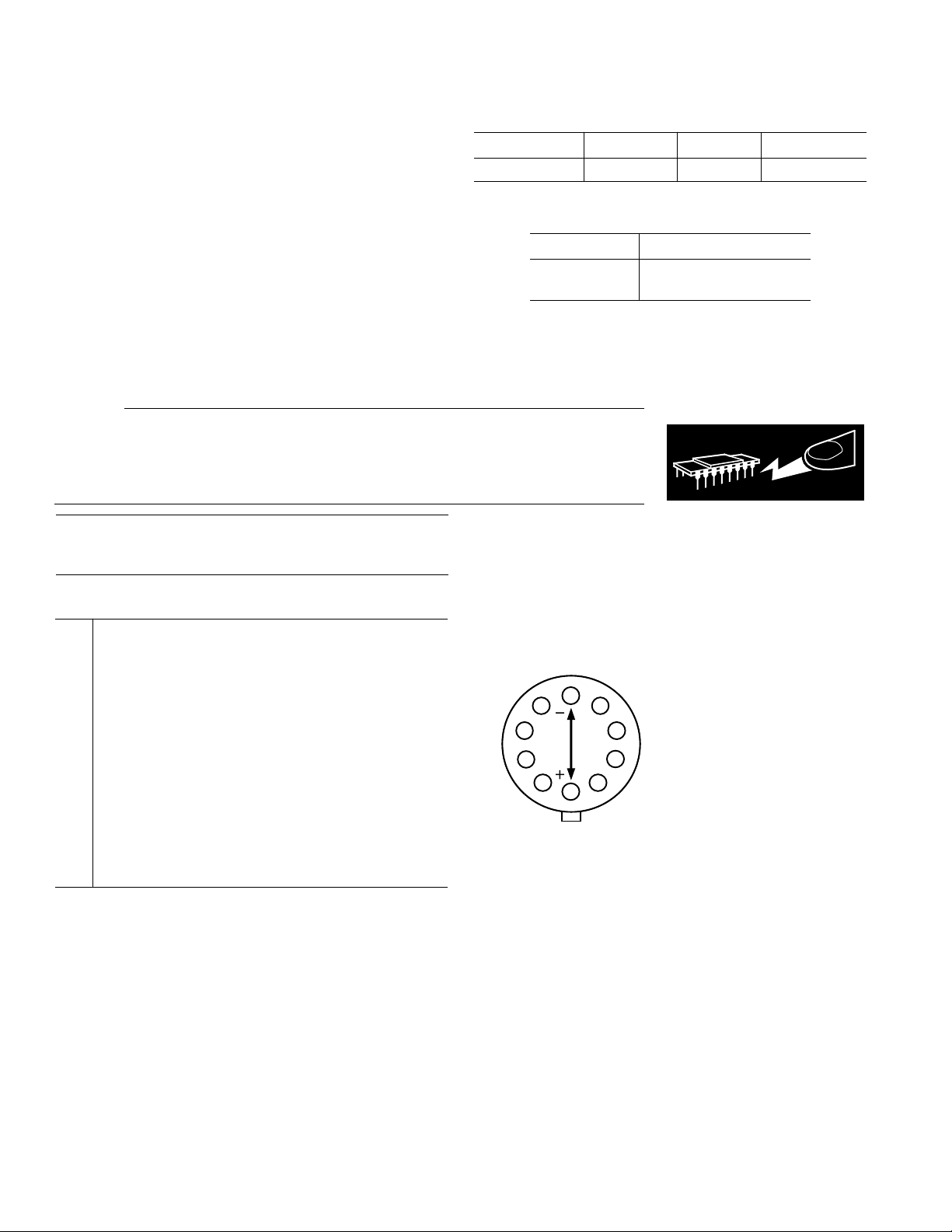
CONNECTION DIAGRAM
10-Header (TO-100)
TOP VIEW
OUT
COM
6
6
7
7
AXIS OF
AXIS OF
8
8
9
9
5
5
SENSITIVITY
SENSITIVITY
10
10
V
IN–
C2
4
4
C1
3
3
2
2
1
1
+5V
NOTES:
C1
AXIS OF SENSITIVITY IS ALONG A LINE
BETWEEN PIN 5 AND THE TAB.
THE CASE OF THE METAL CAN
PACKAGE IS CONNECTED TO PIN 5
(COMMON).
ARROW INDICATES DIRECTION OF
POSITIVE ACCELERATION ALONG AXIS
OF SENSITIVITY.
V
REF
ST
V
PR
V
–4–
REV. B
Page 5
ADXL05
+1g
INDICATED POLARITY IS THAT
OCCURRING AT V
PR
.
TAB
PIN 5
+
–
GLOSSARY OF TERMS
Acceleration: Change in velocity per unit time.
Acceleration Vector: Vector describing the net acceleration
acting upon the ADXL05 (A
XYZ
).
g: A unit of acceleration equal to the average force of gravity
occurring at the earth’s surface. A g is approximately equal to
32.17 feet/s
2
, or 9.807 meters/s2.
Nonlinearity: The maximum deviation of the ADXL05 output
voltage from a best fit straight line fitted to a plot of acceleration
vs. output voltage, calculated as a % of the full-scale output
voltage (@ 5 g).
Resonant Frequency: The natural frequency of vibration of
the ADXL05 sensor’s central plate (or “beam”). At its resonant
frequency of 12 kHz, the ADXL05’s moving center plate has a
peak in its frequency response with a Q of 3 or 4.
Sensitivity: The output voltage change per g unit of accelera-
tion applied, specified at the V
pin in mV/g.
PR
Sensitive Axis (X): The most sensitive axis of the accelerometer sensor. Defined by a line drawn between the package tab
and Pin 5 in the plane of the pin circle. See Figures 2a and 2b.
Sensor Alignment Error: Misalignment between the
ADXL05’s on-chip sensor and the package axis, defined by
Pin 5 and the package tab.
Total Alignment Error: Net misalignment of the ADXL05’s
on-chip sensor and the measurement axis of the application.
This error includes errors due to sensor die alignment to the
package, and any misalignment due to installation of the sensor
package in a circuit board or module.
Transverse Acceleration: Any acceleration applied 90° to the
axis of sensitivity.
Transverse Sensitivity Error: The percent of a transverse acceleration that appears at the V
output. For example, if the
PR
transverse sensitivity is 1%, then a +10 g transverse acceleration
will cause a 0.1 g signal to appear at V
(1% of 10 g). Trans-
PR
verse sensitivity can result from a sensitivity of the sensor to
transverse forces or from misalignment of the internal sensor to
its package.
Transverse Y Axis: The axis perpendicular (90°) to the pack-
age axis of sensitivity in the plane of the package pin circle. See
Figure 2.
Transverse Z Axis: The axis perpendicular (90°) to both the
package axis of sensitivity and the plane of the package pin
circle. See Figure 2.
Polarity of the Acceleration Output
The polarity of the ADXL05 output is shown in the Figure 1.
When oriented to the earth’s gravity (and held in place), the
ADXL05 will experience an acceleration of +1 g. This corresponds to a change of approximately +200 mV at the V
PR
output pin. Note that the polarity will be reversed to a negative
going signal at the buffer amplifier output V
, due to its
OUT
inverting configuration.
Figure 1. Output Polarity at V
PR
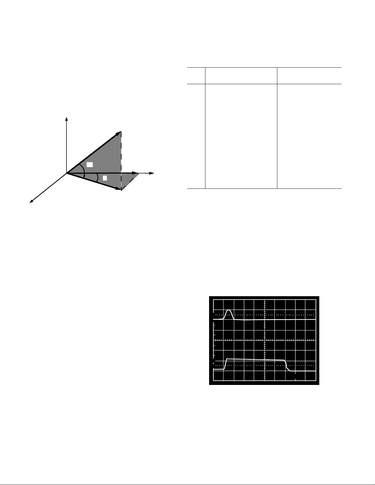
Acceleration Vectors in Three Dimensions
The ADXL05 is a sensor designed to measure accelerations that
result from an applied force. The ADXL05 responds to the
component of acceleration on its sensitive X axis. Figures 2a
and 2b show the relationship between the sensitive “X” axis and
the transverse “Z” and “Y” axes as they relate to the TO-100
Z
SIDE VIEW
X
PIN 5
TRANSVERSE Z AXIS
TAB
Z
X
SENSITIVE (X) AXIS
Figure 2a. Sensitive X and Transverse Z Axis
Y
TOP VIEW
X
PIN 5
TRANSVERSE Y AXIS
SENSITIVE (X) AXIS
TAB
X
REV. B
Y
Figure 2b. Sensitive X and Transverse Y Axis
–5–
Page 6
ADXL05
10
90
100
0%
0.5ms
package. Figure 2c describes a three dimensional acceleration
vector (A
component of interest. To determine A
of acceleration in the XY plane (A
) which might act on the sensor, where AX is the
XYZ
, first, the component
X
) is found using the cosine
XY
law:
A
= A
XY
A
Therefore: Nominal V
–Z AXIS
Y AXIS
(cosθXY) then
XYZ
= AXY (cosθX)
X
= 200 mV/g (A
PR
θxy
θx
Axy
) (cosθXY) cosθ
XYZ
Axyz
Ax
X
X AXIS
Figure 2c. A Vector Analysis of an Acceleration Acting
Upon the ADXL05 in Three Dimensions
Note that an ideal sensor will react to forces along or at angles
to its sensitive axis but will reject signals from its various transverse axes, i.e., those exactly 90° from the sensitive “X” axis.
But even an ideal sensor will produce output signals if the transverse signals are not exactly 90° to the sensitive axis. An acceleration that is acting on the sensor from a direction different
from the sensitive axis will show up at the ADXL05 output at a
reduced amplitude.
Table I shows the percentage signals resulting from various θ
X
angles. Note that small errors in alignment have a negligible
effect on the output signal. A 1° error will only cause a 0.02%
error in the signal. Note, however, that a signal coming 1° off of
the transverse axis (i.e., 89° off the sensitive axis) will still contribute 1.7% of its signal to the output. Thus large transverse
signals could cause output signals as large as the signals of
interest. Table I may also be used to approximate the effect of
the ADXL05’s internal errors due to misalignment of the die to
the package. For example: a 1 degree sensor alignment error will
allow 1.7% of a transverse signal to appear at the output.
Table I. Ideal Output Signals for Off Axis Applied
Accelerations Disregarding Device Alignment and
Transverse Sensitivity Errors
% of Signal Appearing Output in gs for a 5 g
θ
X
at Output Applied Acceleration
0 100% 5.000 (On Axis)
1° 99.98% 4.999
2° 99.94% 4.997
3° 99.86% 4.993
5° 99.62% 4.981
10° 98.48% 4.924
30° 86.60% 4.330
45° 70.71% 3.536
60° 50.00% 2.500
80° 17.36% 0.868
85° 8.72% 0.436
87° 5.25% 0.263
88° 3.49% 0.175
89° 1.7% 0.085
90° 0% 0.000 (Transverse Axis)
Mounting Fixture Resonances
A common source of error in acceleration sensing is resonance
of the mounting fixture. For example, the circuit board that the
ADXL05 mounts to may have resonant frequencies in the same
range as the signals of interest. This could cause the signals
measured to be larger than they really are. A common solution
to this problem is to dampen these resonances by mounting the
ADXL05 near a mounting post or by adding extra screws to
hold the board more securely in place.
When testing the accelerometer in your end application, it is
recommended that you test the application at a variety of frequencies in order to ensure that no major resonance problems
exist (refer to Analog Devices Application Note AN-379).
Figure 3. 500 g Shock Overload Recovery. Top Trace, PCB
Reference Accelerometer Output: 500 g/Vertical Division.
Bottom Trace, ADXL05 Output at V
–6–
PR
REV. B
Page 7

ADXL05
Typical Characteristics
9
6
3
0
–3
–6
–9
–12
–15
NORMALIZED SENSITIVITY – dB
–18
–21
1 10k10
FREQUENCY – Hz
(@ +258C, C1 = C2 = 0.022 mF, VS = +5 V unless otherwise noted)
100 1k
Figure 4. Normalized Sensitivity vs. Frequency
2
1
0
0.2
0.1
0
–0.1
NONLINEARITY IN % OF FULL SCALE
–0.2
05
1234
g LEVEL APPLIED
Figure 7. % Nonlinearity vs. g Level Applied
40
30
20
–1
–2
–3dB BANDWIDTH CHANGE – %
–3
–4
–50 1500 50 100
TEMPERATURE – °C
Figure 5. –3 dB Bandwidth vs. Temperature
0.30
0.20
0.10
0.00
–0.10
–0.20
–0.30
SENSITIVITY CHANGE – %
–0.40
–0.50
4.0 7.54.5 5.0 5.5 6.0 6.5 7.0
SUPPLY VOLTAGE – Volts
10
0
CHANGE IN NOISE – %
–10
–20
–50 1500 50 100
TEMPERATURE – °C
Figure 8. % Change in Noise from +25°C vs. Temperature
10k
1k
100
–3dB BANDWIDTH – Hz
10
0.01
DEMODULATOR CAPACITANCE – µF
10.1
Figure 6. Sensitivity Change at VPR vs. Supply Voltage
REV. B
Figure 9. –3 dB Bandwidth vs. Demodulator
Capacitance
–7–
Page 8

ADXL05
FREQUENCY – Hz
100
80
0
10 10k100 1k
60
40
20
TA = +25°C, ACL = 2
OUTPUT IMPEDANCE – Ω
Typical Characteristics
80
60
E
40
B
20
C
D
0
–20
A
CHANGE IN 0g BIAS LEVEL – mV
–40
–60
–40 120
04080
TEMPERATURE – °C
(@ +258C, C1 = C2 = 0.022 mF, VS = +5 V unless otherwise noted)
A
B
C
D
E
Figure 10. Change in 0 g Bias Level vs. Temperature
(Characteristic Curves from Five Typical Units)
40
30
80
TA = +25°C
= +5V + (0.5Vp-p)
V
S
60
PSRR – dB
REF
40
+3.4V V
20
1 100k10
Figure 13. +3.4 V V
100 1k 10k
FREQUENCY – Hz
PSRR vs. Frequency
REF
20
10
0 g PSRR – dB
PR
NOTE: AT THIS FREQUENCY, THE SIGNAL ON THE
0
V
POWER SUPPLY IS IN SYNCHRONISM WITH THE
ACCELEROMETER'S INTERNAL CLOCK OSCILLATOR
(SEE EMI/RFI SECTION)
–10
–20
10 1M100 1k 10k 100k
Figure 11. 0 g PSRR vs. Frequency
FREQUENCY – Hz
Figure 14. Buffer Amplifier Output Impedance vs.
Frequency
0.05
0
–0.05
–0.1
DRIFT FROM +25°C
–0.15
REF
% V
–0.2
–0.25
–50 1500 50 100
TEMPERATURE – °C
30
25
20
15
10
5
GAIN – dB
0
–5
–10
–15
–20
10 1M100
G =10
G = 2
1k 10k 100k
FREQUENCY – Hz
TA = +25°C
Figure 12. % V
Drift vs. Temperature
REF
–8–
Figure 15. Buffer Amplifier Closed-Loop Gain vs.
Frequency
REV. B
Page 9

ADXL05
BEAM
FIXED
OUTER
PLATES
UNIT CELL
CS1
<
CS2
TOP VIEW
APPLIED
ACCELERATION
CS1
CS2
DENOTES ANCHOR
CENTER PLATE
THEORY OF OPERATION
The ADXL05 is a complete acceleration measurement system
on a single monolithic IC. It contains a polysilicon surfacemicro machined sensor and signal conditioning circuitry which
implements a force-balance control loop. The ADXL05 is capable of measuring both positive and negative acceleration to a
maximum level of ±5 g.
Figure 16 is a simplified view of the ADXL05’s acceleration
sensor at rest. The actual structure of the sensor consists of 46
unit cells and a common beam. The differential capacitor sensor
consists of independent fixed plates and central plates attached
to the main beam that moves in response to an applied acceleration. The two capacitors are series connected, forming a
capacitive divider with a common movable central plate. The
sensor’s fixed capacitor plates are driven differentially by a
1 MHz square wave: the two square wave amplitudes are equal
but are 180° out of phase from one another. When at rest, the
values of the two capacitors are the same, and therefore, the
voltage output at their electrical center (i.e., at the center plate)
is zero.
BEAM
CENTER PLATE
FIXED
OUTER
PLATES
UNIT CELL
CS1
CS2
CS1 = CS2
DENOTES ANCHOR
Figure 16. A Simplified Diagram of the ADXL05
Sensor at Rest
Figure 17 shows the sensor responding to an applied acceleration. When this occurs, the common central plate or “beam”
moves closer to one of the fixed plates while moving further
from the other. This creates a mismatch in the two capacitances,
resulting in an output signal at the central plate. The output
amplitude of the signal varies directly with the amount of acceleration experienced by the sensor.
Figure 17. The ADXL05 Sensor Momentarily Responding
to an Externally Applied Acceleration
Figure 18 shows a block diagram of the ADXL05. The voltage
output from the central plate of the sensor is buffered and then
applied to a synchronous demodulator which is clocked, in
phase, with the same oscillator that drives the fixed plates
of the sensor. If the applied voltage is in sync and in phase
with the clock, a positive output will result. If the applied voltage is in sync but 180° out of phase with the clock, then the
demodulator’s output will be negative. All other signals will be
rejected. An external capacitor, C1, sets the bandwidth of the
demodulator.
REV. B
C2
EXTERNAL
OSCILLATOR
DECOUPLING
CAPACITOR
+5V
V
REF
+3.4V
DENOTES EXTERNAL
PIN CONNECTION
1MHz
OSCILLATOR
+5V
+5V
INTERNAL
REFERENCE
+3.4V +1.8V +0.2V
180
COMMON
COM
+3.4V
CS1
BEAM
CS2
+0.2V
V
+1.8V
IN–
BUFFER
AMPLIFIER
+1.8V
0
+3.4V
75Ω
°
°
SYNC
Figure 18. Functional Block Diagram
–9–
3MΩ
+5V
33kΩ
C1 C1
DEMODULATION
SYNCHRONOUS
DEMODULATOR
V
OUT
EXTERNAL
CAPACITOR
50kΩ
33kΩ
SELF–TEST
(ST)
PREAMP
+1.8V
LOOP GAIN = 10
RST
+3.4V
V
PR
INTERNAL
FEEDBACK
LOOP
Page 10

ADXL05
The output of the synchronous demodulator drives the
preamp—an instrumentation amplifier buffer which is referenced to +1.8 volts. The output of the preamp, V
, is fed back
PR
to the outer plate of the sensor through a 3 MΩ isolation resistor. The V
voltage electrostatically resets the sensor back to its
PR
0 g position and is a direct measure of the applied acceleration.
The output of the ADXL05’s preamplifier is 1.8 V ± 200 mV/g,
with an output range of ±1 V for a ±5 g input. An uncommitted buffer amplifier provides the capability to adjust the scale
factor and 0 g offset level over a wide range. An internal reference supplies the necessary regulated voltages for powering the
chip and +3.4 volts for external use.
A self-test is initiated by applying a TTL “high” level voltage
(> +2.0 V dc) to the ADXL05’s self-test pin, which causes the
chip to apply a deflection voltage to the beam which moves it an
ADXL05
OSCILLATOR
DECOUPLING
CAPACITOR
C2
0.022µF
4
OSCILLATOR
SENSOR
DEMODULATOR
amount equal to –5 g (the negative full-scale output of the device). Note that the ±15% tolerance of the self-test circuit is not
proportional to the sensitivity error, see Self-Test section.
BASIC CONNECTIONS FOR THE ADXL05
Figure 19 shows the basic connections needed for the ADXL05
to measure accelerations in the ±5 g range with an output scale
factor 400 mV/g, a 2.5 V 0 g level, a ± 2.0 V full-scale swing
around 0 g, and a 3 dB bandwidth of approximately 1.6 kHz.
Using the circuit of Figure 19, the overall transfer function is:
V
OUT
PREAMP
R3
=
1.8 V – V
()
()
R1
REFERENCE
PR
+1.8V
R3
+
(1.8)
6
+1.8 V
V
REF
OUTPUT
()
R2
+3.4V
SELF-TEST
(ST)
7
COM
5
C3
0.1µF
1
+5V
2
C1
0.022µF
DEMODULATOR
CAPACITOR
83
C1
V
R1
PR
49.9kΩ
10
V
IN–
R2
274kΩ
BUFFER
Figure 19. ADXL05 Application Providing an Output Sensitivity of 400 mV/g,
a +2.5 V 0 g Level and a Bandwidth of 1 kHz
AMP
R3
100kΩ
9
V
OUT
–10–
REV. B
Page 11

BUFFER
AMP
0.1µF
+5V
V
OUT
0.022µF
C1
C1
+3.4V
REF
COM
1.8V
6
8
9
10
1
2
3
4
0.022µF
C2
PRE-AMP
V
PR
R1b
R3
V
IN–
OUTPUT SCALE FACTOR = x V
PR
OUTPUT
V
PR
OUTPUT: 200mV/g
R3
(R1a + R1b)
5
ADXL05
R1a
USING THE INTERNAL BUFFER AMPLIFIER TO VARY
THE ACCELEROMETER’S OUTPUT SCALE FACTOR
AND 0 g BIAS LEVEL
The ADXL05 accelerometer has an onboard buffer amplifier
that allows the user to change the output scale factor and 0 g
bias level.
The output scale factor of an accelerometer is simply how many
volts output are provided per g of applied acceleration. This
should not be confused with its resolution. The resolution of the
device is the lowest g level the accelerometer is capable of measuring. Resolution is principally determined by the device noise
and the measurement bandwidth.
The 0 g bias level is simply the dc output level of the accelerometer when it is not in motion or being acted upon by the Earth’s
gravity.
Setting the Accelerometer’s Scale Factor
Figure 20 shows the basic connections for using the onboard
buffer amplifier to increase the output scale factor. The nominal
output level in volts from V
to the g forces applied to the sensor (along its sensitive axis)
times 200 mV/g. The use of the buffer is always recommended,
even if the preset scale factor is adequate, as the buffer helps
prevent any following circuitry from loading down the V
output.
0.022µF
In Figure 20, the output scale factor at Pin 9 (V
put at V
PR
of resistor R3 divided by R1. Choose a convenient scale factor,
keeping in mind that the buffer gain not only amplifies the signal but any noise or drift as well. Too much gain can also cause
the buffer to saturate and clip the output wave form.
The circuit of Figure 20 is entirely adequate for many applications, but its accuracy is dependent on the pretrimmed accuracy
of the accelerometer and this will vary by product type and
grade. For the highest possible accuracy, an external trim is recommended. As shown by Figure 21, this consists of a potentiometer, R1a, in series with a fixed resistor, R1b.
REV. B
(the preamplifier output) is equal
PR
PR
C2
4
0.022µF
C1
C1
COM
ADXL05
PRE-AMP
2
3
5
8
6
+3.4V
REF
OUTPUT SCALE FACTOR = x V
V
OUTPUT: 200mV/g
PR
1.8V
V
PR
10
V
R1
IN–
R3
R1
BUFFER
AMP
R3
OUTPUT
PR
1
+5V
C3
0.1µF
9
V
OUT
Figure 20. Basic Buffer Connections
) is the out-
OUT
times the gain of the buffer, which is simply the value
–11–
ADXL05
Figure 21. External Scale Factor Trimming
Setting the Accelerometer’s 0 g Bias Level, AC Coupled
Response
If a dc (gravity) response is not required—for example in motion
sensing or vibration measurement applications—ac coupling can
be used between the preamplifier output and the buffer input as
shown in Figure 22. The use of ac coupling between V
the buffer input virtually eliminates any 0 g drift and allows the
maximum buffer gain without clipping.
Resistor R1 and capacitor C4 together form a high pass filter
whose corner frequency is 1/(2 π R1 C4). This means that this
simple filter will reduce the signal from V
by 3 dB at the
PR
corner frequency, and it will continue to reduce it at a rate of
6 dB/octave (20 dB per decade) for signals below the corner
frequency.
Note that capacitor C4 should be a nonpolarized, low leakage
type. If a polarized capacitor is used, tantalum types are preferred, rather than electrolytic. With polarized capacitors, V
should be measured on each device and the positive terminal of
the capacitor connected toward either V
or VIN—whichever is
PR
more positive
The 0 g offset level of the ADXL05 accelerometer is preset at
+1.8 V. This can easily be changed to a more convenient level,
such as +2.5 V which, being at the middle of the supply voltage,
provides the greatest output voltage swing.
When using the ac coupled circuit of Figure 22, only a single resistor, R2, is required to swing the buffer output to +2.5 V.
Since the “+” input of the buffer is referenced at +1.8 V, its
summing junction, Pin 10, is also held constant at +1.8 V.
Therefore, to swing the buffer’s output to the desired +2.5 V
0 g bias level, its output must move up +0.7 V (2.5 V – 1.8 V =
0.7 V). Therefore, the current needed to flow through R3 to
cause this change, IR3, is equal to:
IR3 =
0.7 Volts
R3 inOhms
PR
and
PR
Page 12

ADXL05
BUFFER
AMP
0.1µF
+5V
V
OUT
0.022µF
C1
C1
+3.4V
REF
COM
1.8V
8
9
10
1
2
3
4
0.022µF
C2
PRE-AMP
V
PR
R1
R3
V
IN–
5
ADXL05
6
R2
100kΩ
0
g
LEVEL
TRIM
50kΩ
S.F. =
R3
R1
R1 ≥ 20kΩ
V
X
FULL
SCALE
±1
g
±2
g
±4
g
±5
g
mV
per
g
2000
1000
500
400
R1
kΩ
30.1
40.2
40.2
49.2
R3
kΩ
301
200
100
100
RECOMMENDED COMPONENT VALUES FOR
VARIOUS OUTPUT SCALE FACTORS
0.022µF
0.022µF
COM
C2
4
ADXL05
C1
C1
2
3
5
+3.4V
REF
6
PRE-AMP
8
V
PR
C4
1.8V
10
V
R1
IN–
R2
BUFFER
AMP
R3
1
+5V
C3
0.1µF
9
V
OUT
SCALE FACTOR =
1
C4 =
2πR1 FL
FOR A +2.5V 0g LEVEL,
IN AN AC COUPLED
CONFIGURATION,
R2 = 2.57 R3
R3
R1
RECOMMENDED COMPONENT VALUES
FULL
SCALE
RANGE
±2
g
±5
g
±2
g
±5
g
±5
g
SCALE
FACTOR
IN
mV/
g
1000
400
1000
400
400
DESIRED
LOW
FREQUENCY
LIMIT, F
L
30Hz
30Hz
3Hz
1Hz
0.1Hz
R1
IN
kΩ
49.9
127
49.9
127
127
CLOSEST
C4
VALUE
0.10µF
0.039µF
1.0µF
1.5µF
15µF
R3
kΩ
249
249
249
249
249
IN
R2 VALUE
IN kΩ FOR
+2.5V 0
LEVEL
640
640
640
640
640
g
Figure 22. Typical Component Values for AC Coupled
Circuit
In order to force this current through R3, the same current
needs to flow from Pin 10 to ground through resistor R2. Since
Pin 10 is always held at +1.8 V, R2 is equal to:
With a dc coupled connection, any difference between a nonideal +1.8 V 0 g level at V
and the fixed +1.8 V level at the
PR
buffer’s summing junction will be amplified by the gain of the
buffer. If the 0 g level only needs to be approximate and the
buffer is operated a low gain, a single fixed resistor, R2, can still
be used. But to obtain the exact 0 g output desired or to allow
the maximum output voltage swing from the buffer, the 0 g
offset will need to be externally trimmed using the circuit of Figure 23. Normally, a value of 100 kΩ is typical for R2.
The buffer’s maximum output swing should be limited to
±2 volts, which provides a safety margin of ±0.25 volts before
clipping. With a +2.5 volt 0 g level, the maximum gain the
buffer should be set to (R3/R1) equals:
200 mV/gTimes the Max Applied Acceleration ings
2Volts
Note that the value of R1 should be kept as large as possible,
20 kΩ or greater, to avoid loading down the V
output.
PR
The device scale factor and 0 g offset levels can be calibrated using the Earth’s gravity as explained in the section “calibrating
the ADXL05.”
1.8 Volts
R2 =
IR3
Therefore, for an ac coupled connection and a +2.5 V 0 g
output:
1.8 Volts × R3
R2 =
0.7Volts
= 2. 57 × R3
If ac coupling is used, the self-test feature must be monitored at
V
, rather than at the buffer output (since the self test output is
PR
a dc voltage).
Setting the Accelerometer’s 0 g Bias Level, DC Coupled
Response
When a true dc (gravity) response is needed, the output from
the preamplifier, V
For high gain applications, a 0 g offset trim will also be needed.
The external offset trim permits the user to set the 0 g offset
voltage to exactly +2.5 volts, since this is at the center of the +5
volt power supply it will allow the maximum output swing from
the buffer without clipping.
, must be dc coupled to the buffer input.
PR
Figure 23. Typical Component Values for Circuit with
External 0 g Trimming
–12–
REV. B
Page 13

ADXL05
DEVICE BANDWIDTH VS. MEASUREMENT
RESOLUTION
Although an accelerometer is usually specified according to its
full scale (clipping) g level, the limiting resolution of the device,
i.e., its minimum discernible input level, is extremely important
when measuring low g accelerations.
The limiting resolution is predominantly set by the measurement noise “floor” which includes the ambient background
noise and the noise of the ADXL05 itself. The level of the noise
floor varies directly with the bandwidth of the measurement. As
the measurement bandwidth is reduced, the noise floor drops,
improving the signal-to-noise ratio of the measurement and increasing its resolution.
The bandwidth of the accelerometer can be easily reduced by
adding low-pass or bandpass filtering. Figure 24 shows the typical noise vs. bandwidth characteristic of the ADXL05.
100mg
10mg
NOISE LEVEL – rms
1mg
10 1k100
3dB BANDWIDTH – Hz
660mg
66mg
NOISE LEVEL – Peak to Peak
6.6mg
Figure 24. Noise Level vs. 3 dB Bandwidth
The output noise of the ADXL05 scales with the square root of
the measurement bandwidth. With a single pole roll-off, the
equivalent rms noise bandwidth is π divided by 2 or approximately 1.5 times the 3 dB bandwidth. For example, the typical
rms noise of the ADXL05J using a 100 Hz one pole post filter is:
Noise(rms) = 500 µg/ Hz × 100(1.5) = 6,124 µgor6.1 mg rms
For the bandpass filter of Figure 27 where both ac coupling and
low pass filtering are used, the low frequency roll-off, F
termined by C4 and R1 and the high frequency roll-off, F
, is de-
L
, is
H
determined by the 1-pole post filter R3, C5.
The equivalent rms noise of the bandpass filter is equal to
500 µg/ Hz × (1.5 FH)–(FL/1.5).
For example, the typical rms noise of the ADXL05 using 1 pole
ac coupling with a bandwidth of 10 Hz and 1 pole low-pass
filter of 100 Hz is:
Noise (rms) = 500 µg/ Hz × 1. 5(100 ) – (10 /1.5)
= 5,987 µg rms or ≈ 5.9 mg rms
Because the ADXL05’s noise is for all practical purposes
Gaussian in amplitude distribution, the highest noise amplitudes
have the smallest (yet nonzero) probability. Peak-to-peak noise
is therefore difficult to measure and can only be estimated due
to its statistical nature. Table II is useful for estimating the
probabilities of exceeding various peak values, given the rms
value.
Table II.
Nominal Peak-to- % of Time that Noise Will Exceed
Peak Value Nominal Peak-to-Peak Value
2.0 × rms 32%
4.0 × rms 4.6%
6.0 × rms 0.27%
6.6 × rms 0.1%
8.0 × rms 0.006%
RMS and peak-to-peak noise (for 0.1% uncertainty) for various
bandwidths is estimated in Figure 24. As shown by the figure,
device noise drops dramatically as the operating bandwidth is
reduced. For example, when operated in a 1 kHz bandwidth,
the ADXL05 typically has an rms noise level of 19 mg. With
±5 g applied accelerations, this 19 mg resolution limit is nor-
mally quite satisfactory; but for smaller acceleration levels the
noise is now a much greater percentage of the signal. As shown
by the figure, when the device bandwidth is rolled off to 100 Hz,
the noise level is reduced to approximately 6 mg, and at 10 Hz it
is down to less than 2 mg.
Alternatively, the signal-to-noise ratio may be improved considerably by using a microprocessor to perform multiple measurements and then compute the average signal level. When using
this technique, with 100 measurements, the signal-to-noise ratio
will be increased by a factor of 10 (20 dB).
REV. B
–13–
Page 14

ADXL05
Low-Pass Filtering
The bandwidth of the accelerometer can easily be reduced by
using post filtering. Figure 25 shows how the buffer amplifier
can be connected to provide 1-pole post filtering, 0 g offset trimming, and output scaling. The table provides practical component values for various full-scale g levels and approximate circuit
bandwidths. For bandwidths other than those listed, use the
formula:
C4=
(2 πR3) Desired 3dBBandwidth in Hz
or simply scale the value of capacitor C4 accordingly, i.e., for an
application with a 50 Hz bandwidth, the value of C4 will need
to be twice as large as its 100 Hz value. If further noise reduction is needed while maintaining the maximum possible bandwidth, then a 2- or 3-pole post filter is recommended. These
provide a much steeper roll-off of noise above the pole frequency. Figure 26 shows a circuit that uses the buffer amplifier
to provide 2-pole post filtering. Component values for the 2pole filter were selected to operate the buffer at unity gain. Capacitors C3 and C4 were chosen to provide 3 dB bandwidths of
10 Hz, 30 Hz, 100 Hz, and 300 Hz.
In this configuration, the nominal buffer amplifier output will be
+1.8 V ± the 200 mV/g scale factor of the accelerometer. An
AD820 external op amp allows noninteractive adjustment of 0 g
offset and scale factor. The external op amp offsets and scales
the output to provide a +2.5 V ± 2 V output over a wide range
of full-scale g levels.
C2
4
ADXL05
PRE-AMP
2
3
5
8
6
V
PR
OPTIONAL SCALE
FACTOR TRIM
R2
COMPONENT VALUES FOR VARIOUS
mV
3dB
per
g
BW (Hz)
2000
10
1000
100
500
200
400
300
3dB BW =
0.022µF
0.022µF
C1
C1
COM
+3.4V
REF
g
0
LEVEL
50kΩ
TRIM
FULL-SCALE RANGES AND BANDWIDTHS
FULL
SCALE
g
±1
±2
g
±4
g
±5
g
1
1
+5V
1.8V
BUFFER
AMP
R1a
kΩ
10
10
10
10
R1b
*
R1b
kΩ
24.9
35.7
35.7
45.3
1
2π R3 C4
10
V
IN–
R3
C4
R2
R3
kΩ
kΩ
100
301
100
200
100
100
100
100
R1a
*TO OMIT THE OPTIONAL SCALE FACTOR
TRIM, REPLACE R1a AND R1b WITH A FIXED
VALUE 1% METAL FILM RESISTOR.
SEE VALUES SPECIFIED IN TABLES BELOW.
NOTE: FOR NONINTERACTIVE TRIMS,
SET SCALE FACTOR FIRST, THEN OFFSET.
9
C4
µF
0.056
0.0082
0.0082
0.0056
0.1µF
V
OUT
ADXL05
8
V
PR
R1
82.5kΩ
0.027
0.082
1.8V
10
V
C3µF
0.27
0.82
PRE-AMP
6
V
REF
2-POLE FILTER
COMPONENT VALUES
3dB
BW (Hz)
300
100
30
10
BUFFER
AMP
C4
IN–
R5
42.2kΩ
R3
C3
82.5kΩ
2-POLE FILTER
+3.4V
R6
40.2kΩ
20kΩ
R7
71.5kΩ
C4µF
0.0033
0.01
0.033
0.1
V
OUT
9
R4a
SCALE
FACTOR
0
g
LEVEL
TRIM
AMPLIFIER COMPONENT VALUES
FULL
SCALE
±1
g
±2
g
±4
g
±5
g
OPTIONAL CAPACITOR
FOR 3-POLE FILTERING
R5
+5V
R4b
2
AD820
mV
per
2000
1000
500
400
3
GAIN
10.00
4.98
2.50
2.00
R4a
kΩ
10
10
10
10
g
TRIM
OFFSET AND SCALING
0.01µF
7
6
4
OFFSET AND
SCALING
AMPLIFIER
R4b
kΩ
24.9
35.7
35.7
45.3
OUTPUT
R5
kΩ
301
200
100
100
Figure 26. Two-Pole Filtering Circuit with Gain and 0 g
Offset Adjustment
Bandpass Filtering
Figure 27 shows how the combination of ac coupling and lowpass filtering together form a bandpass filter that provides an
even greater improvement in noise reduction.
SCALE
FACTOR
IN
mV/
1000
200
1000
200
200
COMPONENT
VALUES ARE
APPROXIMATE.
DESIRED
LOW
FREQUENCY
LIMIT, F
g
30
30
3
1
0.1
ADXL05
PRE-AMP
V
PR
8
V
PR
CLOSEST
R1
VALUE
VALUE
IN kΩ
L
49.9
0.10µF
249
0.022µF
49.9
1.0µF
249
0.68µF
249
6.8µF
C4
C4
1.8V
10
V
R1
R2
DESIRED
HIGH
FREQUENCY
LIMIT, F
300
300
100
100
BUFFER
IN–
10
AMP
H
R3
C5
R3
IN
kΩ
249
249
249
249
249
V
OUT
9
CLOSEST
VALUE
0.002µF
0.002µF
0.0068µF
0.0068µF
0.068µF
VALUE
OF R2
C5
FOR +2.5V
0
g
LEVEL
640kΩ
640kΩ
640kΩ
640kΩ
640kΩ
Figure 25. Using the Buffer Amplifier to Provide 1-Pole
Post Filtering Plus Scale Factor and 0 g Level Trimming
–14–
Figure 27 AC Coupling and Low-Pass Filtering Used
Together to Provide a Bandpass Function
REV. B
Page 15

Additional Noise Reduction Techniques
Shielded wire should be used for connecting the accelerometer to
any circuitry that is more than a few inches away—to avoid 60 Hz
pickup from ac line voltage. Ground the cable’s shield at only one
end and connect a separate common lead between the circuits;
this will help to prevent ground loops. Also, if the accelerometer
is inside a metal enclosure, this should be grounded as well.
Methods for Reducing 0 g Offset Drift
When using any accelerometer with a dc (gravity sensing) response, the 0 g offset level will exhibit some temperature drift.
For very high accuracy applications, one very straightforward
approach is to use a low cost crystal oven to maintain the accelerometer at a constant temperature. These ovens are available in
a variety of different temperatures. After the circuit has been built
and is operating correctly, the crystal oven can be mounted over
the accelerometer and powered off the same +5 V power supply.
The ovens may be purchased from Isotemp Research, Inc., P.O.
Box 3389, Charlottesville, VA 22903, phone 804-295-3101. For
more details on crystal oven compensation, refer to application
note AN-385.
Other methods for 0 g drift compensation include using a low
cost temperature sensor such as the AD22100 to supply a microprocessor with the device temperature. If the drift curve of
the accelerometer is stored in the µP, then a software program
can be used to subtract out the drift. Alternatively, a simple 1st
order (straight line) correction circuit can be used to subtract
out the linear portion of the accelerometer’s drift by using a
temperature sensor and op amp to supply a small compensation
current. For more details on software and hardware drift compensation, refer to application note AN-380.
ACCELEROMETER APPLICATIONS
Popular applications for low g accelerometers tend to fall into
three categories: measurement of tilt and orientation, inertial
measurement of acceleration, velocity and distance, and vibration or shock measurement.
The ADXL05 is a “dc” accelerometer, meaning that it is capable of measuring static accelerations such as the Earth’s gravity. The ADXL05 differs from other acceleration measurement
technologies such as piezoelectric and piezofilm sensors which
can only respond to ac signals greater than approximately 1 Hz.
This dc capability is required for tilt and inertial measurement.
For ac shock or vibration the ADXL05 can measure frequencies
of up to 4 kHz and has the added benefit of measuring all the
way down to dc.
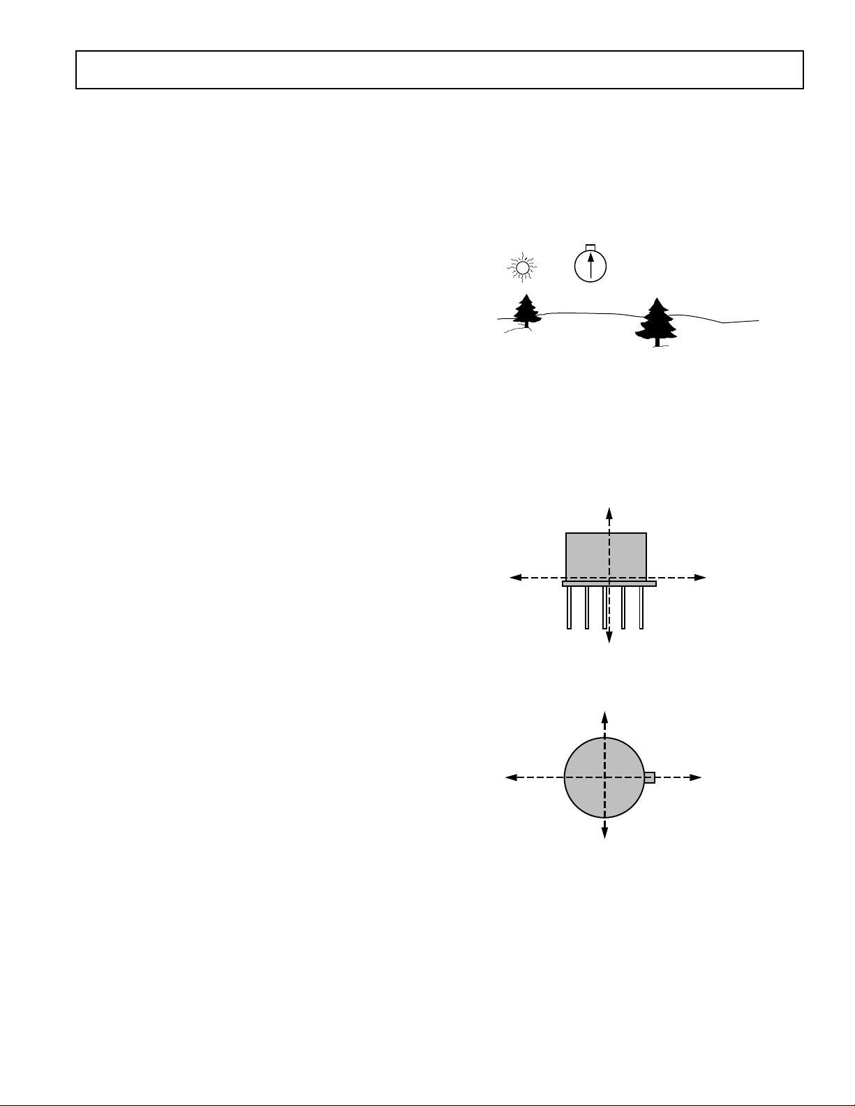
Using the ADXL05 in Tilt Applications
The ADXL05’s precision dc characteristics make it suitable for
tilt measurement. It can directly measure the Earth’s gravity and
use this constant force as a position reference to determine inclination. As shown in Figure 28, the accelerometer should be
mounted so that its sensitive axis is perpendicular to the force of
gravity, i.e., parallel to the Earth’s surface. In this manner, it
will be most sensitive to changes in orientation (when it is orientated 90° to the force of gravity). Its output can be then described by the sine function; a tilt occurring at an angle θ will
cause a voltage output equal to:
V
V
= Accelerometer Scale Factor
OUT
g
×sin
θ
×1g
()
+zero g output(V )
ADXL05
θ
1g
Figure 28. Two Possible Orientations for Tilt Measurement
Conversely, for a given acceleration signal and assuming no
other changes in the axis or interfering signals, the tilt angle is
proportional to the voltage output as shown in Figure 29. The
angle, θ can be calculated using:
θ
= arcsin 1g ×
500
400
300
200
g
100
0
@ 500mV/
–100
OUT
V
–200
–300
–400
–500
–90 90–70 –50 –30 –10
Figure 29. V
OUT
Scale Factor (V/g)
ANGLE OF TILT
vs. Tilt Angle
OUT
–zero g output(V)
V
The use of an accelerometer in tilt applications has several advantages over the use of a traditional tilt sensor. A traditional tilt
sensor consists of glass vial filled with a conductive liquid, typically a mercury or electrolytic solution. Besides being larger
than an XL05, it requires additional signal conditioning circuitry. The settling time and frequency response is limited by
the amount of time required for the liquid to stop sloshing
around in the vial. In high vibration environments, or where
high lateral accelerations may be present, it may not be possible
to resolve the tilt signal above the “slosh” noise. The accelerometer has faster frequency (up to 50 ×) response and settling time. Interfering vibrations may be filtered out if
necessary, an impossibility with a liquid tilt sensor, since one
cannot filter the liquid. Finally, in the presence of lateral accelerations, an accelerometer provides more useful information,
i.e., an acceleration signal, which if cleverly signal processed,
can provide both a tilt and an acceleration output. A single accelerometer can be used to measure tilt over a 180° range; two
accelerometers gives a complete 360° of measurement.
An important characteristic for an accelerometer used in a tilt
application is its 0 g offset stability over temperature. The
ADXL05 typically exhibits offsets that deviate no more than
0.1 g over the 0°C to +70°C temperature range, corresponding
θ
1g
10 30 50 70
REV. B
–15–
Page 16

ADXL05
0
g
(a)
0
g
(b)
–1
g
(c)
+1
g
(d)
INDICATED POLARITY IS THAT
OCCURRING AT V
PR
.
to a 5° tilt error over the entire temperature range. Straightforward calibration schemes discussed in this data sheet may be
used to reduce or compensate for temperature drift to improve
the absolute accuracy of the measurement.
Using the ADXL05 in Inertial Measurement Applications
Inertial measurement refers to the practice of measuring acceleration for the purpose of determining the velocity of an object
and its change in position, or distance traveled. This technique
has previously required expensive inertial guidance systems of
the type used in commercial aircraft and military systems. The
availability of a low cost precision dc accelerometer such as the
ADXL05 enables the use of inertial measurement for more cost
sensitive industrial and commercial applications.
Inertial measurement makes use of the fact that the integral of
acceleration is velocity and the integral of velocity is distance.
By making careful measurements of acceleration and mathematically integrating the signals, one can determine both velocity and the distance traveled. The technique is useful for
applications where a traditional speed and distance measurement is impractical, or where a non-contact, relative position
measurement must be made.
A practical inertial measurement system uses multiple accelerometers to measure acceleration in three axes, and gyroscopes to
measure rotation in three axes, the requirement for a 6 degree of
freedom system. For simpler systems where one or more of the
axes can be constrained, it is possible to build a system with
fewer accelerometers and gyros.
The measurement system must take the acceleration sensor and
calibrate out all static errors including any initial inaccuracy or
temperature drift. A mathematical model is used to describe the
performance of the sensor in order to calibrate it. If these errors
are not removed, then the process of double integration will
quickly cause any small error to dominate the result. Most practical systems use microprocessors for error correction and a temperature sensor for temperature drift compensation. Another
approach is to maintain all of the sensors at a controlled temperature. The microprocessors have the additional advantage of
providing a low cost method of performing the single and
double integration of the acceleration signal.
The stability and repeatability of the accelerometer is the most
important specification in an inertial system. The ADXL05 is
“well behaved” that is, its response and temperature characteristics are easy to model and correct, and once modeled they are
very repeatable. For example, temperature performance can be
adequately modeled using first order, (straight line) approximations for most applications, and other errors such as on-axis and
pendulous rectification are minimal. This greatly simplifies the
math required to correct the sensor.
Vibration and Shock Measurement Applications
The ADXL05 can measure shocks and vibrations from dc to
4 kHz. Typical signal processing for vibration signals includes
fast Fourier transforms, and single and double integration for
velocity and displacement. It is possible to build a single integrator stage using the ADXL05’s output buffer amplifier in
order to provide a velocity output.
The sensitivity of the accelerometer will typically vary only
±0.5% over the full industrial temperature range, making it one
of the most stable vibration measurement devices available. In
vibration measurement applications, mechanical mounting and
control of system and mounting resonances are critical to proper
measurement. Refer to the application note AN-379, available
from Analog Devices.
CALIBRATING THE ADXL05
If a calibrated shaker is not available, both the 0 g level and scale
factor of the ADXL05 may be easily set to fair accuracy by using
a self-calibration technique based on the 1 g (average) acceleration of the earth’s gravity. Figure 30 shows how gravity and
package orientation affect the ADXL05’s output. Note that the
output polarity is that which appears at V
; the output at V
PR
OUT
will have the opposite sign. With its axis of sensitivity in the
vertical plane, the ADXL05 should register a 1 g acceleration,
either positive or negative, depending on orientation. With the
axis of sensitivity in the horizontal plane, no acceleration (the
0 g bias level) should be indicated.
Figure 30. Using the Earth’s Gravity to Self-Calibrate the
ADXL05
To self-calibrate the ADXL05, place the accelerometer on its
side with its axis of sensitivity oriented as shown in “a.” The 0 g
offset potentiometer, Rt, is then roughly adjusted for midscale:
+2.5 V at the buffer output (see Figure 25).
Next, the package axis should be oriented as in “c” (pointing
down) and the output reading noted. The package axis should
then be rotated 180° to position “d” and the scale factor potentiometer, R1a, adjusted so that the output voltage indicates a
change of 2 gs in acceleration. For example, if the circuit scale
factor at the buffer output is 400 mV per g, then the scale factor
trim should be adjusted so that an output change of 800 mV is
indicated.
Adjusting the circuit’s scale factor will have some effect on its
0 g level so this should be readjusted, as before, but this time
checked in both positions “a” and “b.” If there is a difference in
the 0 g reading, a compromise setting should be selected so that
the reading in each direction is equidistant from +2.5 V. Scale
factor and 0 g offset adjustments should be repeated until both
are correct.
REDUCING POWER CONSUMPTION
The use of a simple power cycling circuit provides a dramatic
reduction in the ADXL05’s average current consumption. In
low bandwidth applications such as shipping recorders, this
simple, low cost circuit can provide substantial power reduction.
If a microprocessor is available, only the circuit of Figure 31 is
needed. The microprocessor supplies a TTL clock pulse to gate
buffer transistor Q1 which inverts the output pulse from the µP
–16–
REV. B
Page 17

ADXL05
so that the duty cycle is correct when the pulse is re-inverted
again by transistor, Q2, which cycles the accelerometer’s supply
voltage on and off.
+5V
FROM µP
OR
FIGURE 1b
10kΩ
100kΩ
Q1
2N2222
0.1µF
10kΩ
V
PR
58
BUFFER
2N3906
Q2
1
ADXL05
V
10
R1
IN–VOUT
9
R3
C
F
V
OUT
Figure 31. Basic Power Cycling Circuit
Figures 32 and 33 show typical waveforms of the accelerometer
being operated with a 10% duty cycle: 1 ms on, 9 ms off. This
reduces the average current consumption of the accelerometer
from 8 mA to 800 µA, providing a power reduction of 90%. The
µP should sample acceleration during the interval between the
time the 0 g level has stabilized (≈ 400 µs using a 0.022 µF
demod cap) and the end of the pulse duration. The measurement bandwidth of a power-cycled circuit will be set by the
clock pulse rate and duty cycle. In this example, 1 sample can
be taken every 10 ms which is 100 samples per second or 100
Hz. As defined by the “Nyquist criteria,” the best case measurement bandwidth is F
/2 or half the clock frequency. Therefore
S
50 Hz signals can be processed if adequate filtering is provided.
2V
100
90
10
0%
1V
200µs
Figure 32. Top Trace: Voltage at Pin 1;
Bottom Trace: Output at V
PR
Higher measurement bandwidths can be achieved by reducing
the size of the demodulation capacitor below 0.022 µF and in-
creasing the pulse frequency. A 0.01 µF capacitor was con-
nected across the feedback resistor of the ADXL05 buffer to
improve its transient characteristics. The optimum value for this
capacitor will change with buffer gain and the cycling pulse rate.
For more details, refer to application note AN-378.
2V
100
90
10
0%
500mV
200µs
Figure 33. Top Trace: Voltage at Pin 1; Bottom Trace:
Ω
Buffer Output With R1 = R3 = 100 k
, CF = 0.01 µF
COMPONENT SELECTION
LOAD DRIVE CAPABILITIES OF THE VPR AND BUFFER
OUTPUTS
The VPR and the buffer amplifier outputs are both capable of
driving a load to voltage levels approaching that of the supply
rail. However, both outputs are limited in how much current
they can supply, affecting component selection.
VPR Output
The VPR pin has the ability to source current up to 500 µA but
only has a sinking capability of 30 µA which limits its ability to
drive loads. It is recommended that the buffer amplifier be used
in most applications, to avoid loading down V
±5 g applications, the resistor R1 from V
mended to have a value greater than 20 kΩ to reduce loading
effects.
Capacitive loading of the V
capacitance between the V
pin should be minimized. A load
PR
pin and common will introduce an
PR
offset of approximately 1 mV for every 10 pF of load. The V
pin may be used to directly drive an A/D input or other source
as long as these sensitivities are taken into account. It is always
preferable to drive A/D converters or other sources using the
buffer amplifier (or an external op amp) instead of the V
Buffer Amplifier Output
The buffer output can drive a load to within 0.25 V of either
power supply rail and is capable of driving 1000 pF capacitive
loads. Note that a capacitance connected across the buffer
feedback resistor for low-pass filtering does not appear as a
capacitive load to the buffer. The buffer amplifier is limited to
sourcing or sinking a maximum of 100 µA. Component values
for the resistor network should be selected to ensure that the
buffer amplifier can drive the filter under worst case transient
conditions.
Self-Test Function
The digital self-test input is compatible with both CMOS and
TTL signals. A Logic “l” applied to the self-test (ST) input will
cause an electrostatic force to be applied to the sensor which
will cause it to deflect to the approximate negative full-scale
output of the device. Accordingly, a correctly functioning accelerometer will respond by initiating an approximate –1 volt
PR
to V
. In standard
PR
is recom-
IN–
PR
PR
pin.
REV. B
–17–
Page 18

ADXL05
output change at V
acceleration when the self-test is initiated, the V
. If the ADXL05 is experiencing an
PR
output will
PR
equal the algebraic sum of the two inputs. The output will stay
at the self-test level as long as the ST input remains high and
will return to the 0 g level when the ST voltage is removed.
A self-test output that varies more than ± 15% from the nominal
–1.0 V change indicates a defective beam or a circuit problem
such as an open or shorted pin or component.
Operating the ADXL05’s buffer amplifier at Gains > 2, to provide full-scale outputs of less than ± 5 g, may cause the self-test
output to overdrive the buffer into saturation. The self-test may
still be used in the case, but the change in the output must then
be monitored at the V
pin instead of the buffer output.
PR
Note that the value of the self-test delta is not an exact indication of the sensitivity (mV/g) of the ADXL05 and, therefore,
may not be used to calibrate the device for sensitivity error.
In critical applications, it may be desirable to monitor shifts in
the zero-g bias voltage from its initial value. A shift in the 0 g
bias level may indicate that the 0 g level has shifted which may
warrant an alarm.
Power Supply Decoupling
The ADXL05 power supply should be decoupled with a 0.1 µF
ceramic capacitor from +5 V pin of the ADXL05 to common
using very short component leads. For other decoupling considerations, see EMI/RFI section.
Oscillator Decoupling Capacitor, C2
An oscillator decoupling capacitor, C2, is used to remove
1 MHz switching transients in the sensor excitation signal, and
is required for proper operation of the ADXL05. A ceramic
capacitor with a minimum value of 0.022 µF is recommended
from the oscillator decoupling capacitor pin to common. Small
amounts of capacitor leakage due to a dc resistance greater than
1MΩ will not affect operation (i.e., a high quality capacitor is
not needed here). As with the power supply bypass capacitor,
very short component leads are recommended. Although
0.022 µF is a good typical value, it may be increased for reasons
of convenience, but doing this will not improve the noise performance of the ADXL05.
Demodulator Capacitor, C1
The demodulator capacitor is connected across Pins 2 and 3 to
set the bandwidth of the force balance control loop. This capacitor may be used to approximately set the bandwidth of the accelerometer. A capacitor is always required for proper operation.
The frequency response of the ADXL05 exhibits a single pole
roll-off response, see Figure 4.
A nominal value of 0.022 µF is recommended for C1. In gen-
eral, the design bandwidth should be set 40% higher than the
minimum desired system bandwidth due to the ± 40% tolerance,
to preserve stability C1 should be kept > 0.01 µF.
The demodulation capacitor should be a low leakage, low drift
ceramic type with an NPO (best) or X7R (good) dielectric.
In general, it’s best to use the recommended 0.022 µF capacitor
across the demodulator pins and perform any additional lowpass filtering using the buffer amplifier. The use of the buffer for
low-pass filtering generally results in smaller capacitance values
and better overall performance. It is also a convenient and more
precise way to set the system bandwidth. Post filtering allows
bandwidth to be controlled accurately by component selection
and avoids the ±40% demodulation tolerance. Note that signal
noise is proportional to the square root of the bandwidth of the
ADXL05 and may be a consideration in component selection—
see section on noise.
Care should be taken to reduce or eliminate any leakage paths
from the demodulator capacitor pins to common or to the +5 V
pin. Even a small imbalance in the leakage paths from these pins
will result in offset shifts in the zero-g bias level. As an example,
an unbalanced parasitic resistance of 30 MΩ from either demodulator pin to ground will result in an offset shift at V
PR
of
approximately 50 mV. Conformal coating of PC boards with a
high impedance material is recommended to avoid leakage problems due to aging or moisture.
MINIMIZING EMI/RFI
The architecture of the ADXL05 and its use of synchronous demodulation make the device immune to most electromagnetic
(EMI) and radio frequency (RFI) interference. The use of synchronous demodulation allows the circuit to reject all signals except those at the frequency of the oscillator driving the sensor
element. However, the ADXL05 does have a sensitivity to RFI
that is within ±5 kHz of the internal oscillator’s nominal frequency of 1 MHz and also to any odd harmonics of this frequency. The internal oscillator frequency will exhibit part to
part variation in the range of 0.5 MHz to 1.4 MHz.
In general the effect is difficult to notice as the interference must
match the internal oscillator within ±5 kHz and must be large
in amplitude. For example: a 1 MHz interference signal of
20 mV p-p applied to the +5 V power supply pin will produce a
200 mV p-p signal at the V
pin if the internal oscillator and
PR
interference signals are matched exactly or at odd harmonics. If
the same 20 mV interference is applied but 5 kHz above or below the internal oscillator’s frequency, the signal level at V
PR
will
only be 20 mV p-p in amplitude.
Power supply decoupling, short component leads (especially for
capacitors C1 and C2), physically small (surface mount, etc.)
components and attention to good grounding practices all help
to prevent RFI and EMI problems. Good grounding practices
include having separate analog and digital grounds (as well as
separate power supplies or very good decoupling) on the printed
circuit boards. A single ground line shared by both the digital
and analog circuitry can lead to digital pulses (and clock signals)
interfering with the sensor’s onboard oscillator. In extreme
cases, a low cost radio frequency choke (≈10 µH) may be
needed in series with the accelerometer’s power supply pin.
This, together with the recommended 0.1 µF power supply by-
pass capacitor, will form an effective RF filter. The use of an RF
choke is preferred over a resistor since any series resistance in
the power supply will “unregulate” the device from the supply,
degrade its power supply rejection and reduce its supply voltage.
–18–
REV. B
Page 19

0.335 (8.51)
0.305 (7.75)
0.370 (9.40)
0.335 (8.51)
0.185 (4.70)
0.165 (4.19)
0.040 (1.02) MAX
0.045 (1.14)
0.010 (0.25)
OUTLINE DIMENSIONS
Dimensions shown in inches and (mm).
REFERENCE PLANE
0.750 (19.05)
0.500 (12.70)
SEATING PLANE
0.115
(2.92)
BSC
0.230 (5.84)
BSC
5
4
3
0.160 (4.06)
0.110 (2.79)
6
2
1
0.034 (0.86)
0.027 (0.69)
7
ADXL05
8
0.045 (1.14)
0.027 (0.69)
9
10
REV. B
–19–
Page 20

C2028b–5–3/96
–20–
PRINTED IN U.S.A.
 Loading...