

Page 1

Six, 11-Bit, 297 MHz DACs
ADV7342/ADV7343
Rev.
Trademarks and registered trademarks are the prop erty of their respective owner s.
Fax: 781.461.3113 ©2006–2012 Analog Devices, Inc. All rights reserved.
D
Data Sheet
FEATURES
74.25 MHz 16-/24-bit high definition input support
Compliant with SMPTE 274M (1080i), 296M (720p),
and 240M (1035i)
Six 11-bit, 297 MHz video DACs
16× (216 MHz) DAC oversampling for SD
8× (216 MHz) DAC oversampling for ED
4× (297 MHz) DAC oversampling for HD
37 mA maximum DAC output current
NTSC M, PAL B/D/G/H/I/M/N, PAL 60 support
NTSC and PAL square pixel operation (24.54 MHz/29.5 MHz)
Multiformat video input support
4:2:2 YCrCb (SD, ED, and HD), 4:4:4 YCrCb (ED and HD), and
4:4:4 RGB (SD, ED, and HD)
Multiformat video output support
Composite (CVBS) and S-Video (Y-C)
Component YPrPb (SD, ED, and HD)
Component RGB (SD, ED, and HD)
Macrovision Rev 7.1.L1 (SD) and Rev 1.2 (ED) compliant
Simultaneous SD and ED/HD operation
EIA/CEA-861B compliance support
Copy generation management system (CGMS)
Closed captioning and wide screen signaling (WSS)
Integrated subcarrier locking to external video source
Complete on-chip video timing generator
On-chip test pattern generation
On-board voltage reference (optional external input)
Programmable features
Luma and chroma filter responses
Vertical blanking interval (VBI)
Subcarrier frequency (F
Luma delay
High definition (HD) programmable features
(720p/1080i/1035i)
4× oversampling (297 MHz)
Internal test pattern generator
Fully programmable YCrCb to RGB matrix
Gamma correction
Programmable adaptive filter control
Programmable sharpness filter control
CGMS (720p/1080i) and CGMS Type B (720p/1080i)
Undershoot limiter
) and phase
SC
Multiformat Video Encoder
Dual data rate (DDR) input support
Enhanced definition(ED) programmable features
(525p/625p)
8× oversampling (216 MHz output)
Internal test pattern generator
Black bar, hatch, flat field/frame
Individual Y and PrPb output delay
Gamma correction
Programmable adaptive filter control
Fully programmable YCrCb to RGB matrix
Undershoot limiter
Macrovision Rev 1.2 (525p/625p) (ADV7342 only)
CGMS (525p/625p) and CGMS Type B (525p)
Dual data rate (DDR) input support
Standard definition (SD) programmable features
16× oversampling (216 MHz)
Internal test pattern generator
Color and black bar
Controlled edge rates for start and end of active video
Individual Y and PrPb output delay
Undershoot limiter
Gamma correction
Digital noise reduction (DNR)
Multiple chroma and luma filters
Luma-SSAF filter with programmable gain/attenuation
PrPb SSAF
Separate pedestal control on component and
composite/S-Video output
VCR FF/RW sync mode
Macrovision Rev 7.1.L1 (ADV7342 only)
Copy generation management system (CGMS)
Wide screen signaling
Closed captioning
Serial MPU interface with I
3.3 V analog operation, 1.8 V digital operation, and 1.8 V or
3.3 V I/O operation
Temperature range: −40°C to +85°C
APPLICATIONS
DVD recorders and players
High definition Blu-ray DVD players
2
C compatibility
Information furnished by Analog Devices is believed to be accurate and reliable. However, no
responsibility is assumed by Analog Devices for its use, nor for any infringements of patents or other
rights of third parties that may result from its use. Specifications subject to ch ange without notice. No
license is granted by implication or otherwise under any patent or patent rights of Analog Devices.
One Technology Way, P.O. Box 9106, Norwood, MA 02062-9106, U.S.A.
Tel: 781.329.4700 www.analog.com
Page 2

ADV7342/ADV7343 Data Sheet
D
TABLE OF CONTENTS
Features .............................................................................................. 1
Applications ....................................................................................... 1
Revision History ............................................................................... 4
General Description ......................................................................... 5
Functional Block Diagram .............................................................. 6
Specifications ..................................................................................... 7
Power Supply and Voltage Specifications .................................. 7
Voltage Reference Specifications ................................................ 7
Input Clock Specifications .......................................................... 7
Analog Output Specifications ..................................................... 8
Digital Input/Output Specifications—3.3 V ............................. 8
Digital Input/Output Specifications—1.8 V ............................. 8
Digital Timing Specifications—3.3 V ........................................ 9
Digital Timing Specifications—1.8 V ...................................... 10
MPU Port Timing Specifications ............................................. 11
Power Specifications .................................................................. 11
Video Performance Specifications ........................................... 12
Timing Diagrams ............................................................................ 13
Absolute Maximum Ratings .......................................................... 20
Thermal Resistance .................................................................... 20
ESD Caution ................................................................................ 20
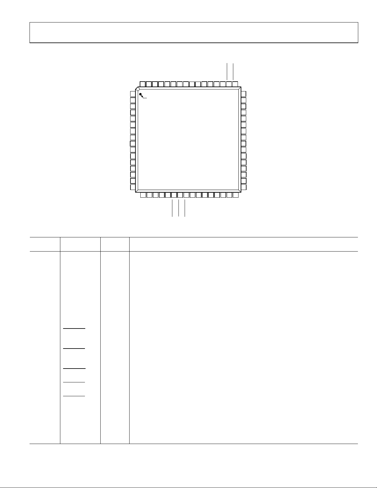
Pin Configuration and Function Descriptions ........................... 21
Typical Performance Characteristics ........................................... 23
MPU Port Description ................................................................... 28
I2C Operation .............................................................................. 28
Register Map Access ....................................................................... 30
Register Programming ............................................................... 30
Subaddress Register (SR7 to SR0) ............................................ 30
Input Configuration ....................................................................... 48
Standard Definition Only .......................................................... 48
Enhanced Definition/High Definition Only .......................... 49
Simultaneous Standard Definition and Enhanced
Definition/High Definition ....................................................... 49
Enhanced Definition Only (at 54 MHz) ................................. 50
Output Configuration .................................................................... 51
Design Features ............................................................................... 52
Output Oversampling ................................................................ 52
HD Interlace External
Considerations ............................................................................ 53
ED/HD Timing Reset ................................................................ 53
P_HSYNC
and
P_VSYNC
SD Subcarrier Frequency Lock ................................................. 53
SD VCR FF/RW Sync ................................................................ 54
Vertical Blanking Interval ......................................................... 54
SD Subcarrier Frequency Control ............................................ 54
SD Noninterlaced Mode ............................................................ 54
SD Square Pixel Mode ............................................................... 55
Filters ............................................................................................ 56
ED/HD Test Pattern Color Controls ....................................... 57
Color Space Conversion Matrix ............................................... 57
SD Luma and Color Scale Control ........................................... 59
SD Hue Adjust Control .............................................................. 59
SD Brightness Detect ................................................................. 59
SD Brightness Control ............................................................... 59
SD Input Standard Autodetection ............................................ 60
Double Buffering ........................................................................ 61
Programmable DAC Gain Control .......................................... 61
Gamma Correction .................................................................... 61
ED/HD Sharpness Filter and Adaptive Filter Controls ......... 63
ED/HD Sharpness Filter and Adaptive Filter Application
Examples ...................................................................................... 64
SD Digital Noise Reduction ...................................................... 65
SD Active Video Edge Control ................................................. 66
External Horizontal and Vertical Synchronization Control . 68
Low Power Mode ........................................................................ 69
Cable Detection .......................................................................... 69
DAC Autopower-Down ............................................................. 69
Sleep Mode .................................................................................. 70
Pixel and Control Port Readback ............................................. 70
Reset Mechanism........................................................................ 70
SD Teletext Insertion ................................................................. 70
Printed Circuit Board Layout and Design .................................. 72
Unused Pins ................................................................................ 72
DAC Configurations .................................................................. 72
Voltage Reference ....................................................................... 72
Video Output Buffer and Optional Output Filter .................. 72
Printed Circuit Board (PCB) Layout ....................................... 73
Typical Application Circuit ....................................................... 75
Copy Generation Management System ....................................... 76
SD CGMS .................................................................................... 76
ED CGMS .................................................................................... 76
Rev. | Page 2 of 108
Page 3

Data Sheet ADV7342/ADV7343
D
HD CGMS .................................................................................... 76
CGMS CRC Functionality ......................................................... 76
SD Wide Screen Signaling .............................................................. 79
SD Closed Captioning .................................................................... 80
Internal Test Pattern Generation ................................................... 81
SD Test Patterns ........................................................................... 81
ED/HD Test Patterns .................................................................. 81
SD Timing ........................................................................................ 82
HD Timing ....................................................................................... 87
Video Output Levels ....................................................................... 88
SD YPrPb Output Levels—SMPTE/EBU N10 ........................ 88
ED/HD YPrPb Output Levels ................................................... 89
SD/ED/HD RGB Output Levels ................................................ 90
SD Output Plots .......................................................................... 91
Video Standards .............................................................................. 92
Configuration Scripts ..................................................................... 94
Standard Definition .................................................................... 94
Enhanced Definition .................................................................. 98
High Definition ......................................................................... 101
Outline Dimensions ...................................................................... 106
Ordering Guide ......................................................................... 106
Rev. | Page 3 of 108
Page 4

ADV7342/ADV7343 Data Sheet
REVISION HISTORY
3/12—Rev. C to Rev. D
Changed ADV7340/ADV7341 to ADV7342/ADV7343 ........... 70
3/12—Rev. B to Rev. C
Reorganized Layout ............................................................ Universal
Change to Features Section ............................................................. 1
Moved Revision History Section .................................................... 4
Change to Table 1 ............................................................................. 5
Changes to Digital Input/Output Specifications—
1.8 V Section ..................................................................................... 8
Changes to Table 15 ........................................................................ 21
Changes to Table 21 ........................................................................ 33
Changes to Table 24 ........................................................................ 36
Changes to Table 29 ........................................................................ 41
Changes to Table 30 ........................................................................ 42
Changes to 24-Bit 4:4:4 RGB Mode Section ............................... 48
Deleted ED/HD Nonstandard Timing Mode Section, Figure 59,
and Table 42, Renumbered Sequentially ..................................... 50
Deleted Subaddress 0x84, Bits[2:1] Section, Timing Reset (TR)
Mode Section, Subcarrier Phase Reset (SCR) Mode
Section, and Figure 60 .................................................................... 51
Deleted Figure 61 ............................................................................ 52
Added External Sync Polarity Section ......................................... 52
Changed SD Subcarrier Frequency Lock, Subcarrier Phase
Reset, and Timing Reset Section to SD Subcarrier Frequency
Lock Section .................................................................................... 53
Changes to ED/HD Test Patterns Section ................................... 81
9/11—Rev. A to Rev. B
Changes to MPU Port Description Section ................................ 27
3/09—Rev. 0 to Rev. A
Changes to Features Section............................................................ 1
Deleted Detailed Features Section, Changes to Table 1............... 4
Changes to Figure 1 .......................................................................... 5
Changes to Table 6 ............................................................................ 7
Added Digital Input/Output Specifications—1.8 V Section and
Table 7 ................................................................................................ 7
Changes to Digital Timing Specifications—3.3 V Section and
Table 8 ................................................................................................ 8
Added Table 9 .................................................................................... 9
Changes to MPU Port Timing Specifications Section,
Default Conditions ......................................................................... 10
Deleted Figure 20 ............................................................................ 18
Changes to Table 13 ........................................................................ 19
Changes to Table 15 ....................................................................... 20
Changes to MPU Port Description Section ................................ 27
Changes to I
2
C Operation Section ............................................... 27
Added Table 16 ............................................................................... 27
Added Figure 49 ............................................................................. 28
Changes to Table 17 ....................................................................... 29
Changes to Table 18 ....................................................................... 29
Changes to Table 21, 0x30 Bit Description ................................. 32
Changes to Table 29 ....................................................................... 39
Changes to Table 30 ....................................................................... 40
Changes to Table 31, 0xA0 Register Name ................................. 42
Changes to Table 32 ....................................................................... 43
Added Table 33 and Table 34 ........................................................ 44
Changes to Standard Definition Only Section ........................... 46
Added Figure 52 ............................................................................. 47
Changes to Figure 53 ...................................................................... 47
Changes to Figure 56, Figure 57, and Figure 58 ......................... 48
Renamed Features Section to Design Features Section ............. 50
Changes to ED/HD Nonstandard Timing Mode Section ......... 50
Changes to Figure 60 ...................................................................... 51
Added HD Interlace External
P_HSYNC
and
P_VSYNC
Considerations Section .................................................................. 51
Changes to SD Subcarrier Frequency Lock, Subcarrier Phase
Reset, and Timing Reset Section .................................................. 51
Changes to Programming the F
Section ................................... 53
SC
Changes to Subaddress 0x8C to Subaddress 0x8F Section ....... 53
Changes to Subaddress 0x82, Bit 4 Section ................................. 53
Added SD Manual CSC Matrix Adjust Feature Section ............ 56
Changes to Subaddress 0x9C to Subaddress 0x9F Section ....... 57
Changes to SD Brightness Detect Section ................................... 58
Changes to Figure 71 ...................................................................... 60
Added Sleep Mode Section ........................................................... 68
Changes to Pixel and Control Port Readback Section .............. 68
Added SD Teletext Insertion Section ........................................... 68
Added Unused Pins Section .......................................................... 70
Added Figure 86 and Figure 87 .................................................... 70
Changes to Power Supply Sequencing Section ........................... 72
Changes to Figure 94 ...................................................................... 75
Changes to SD Wide Screen Signaling Section .......................... 77
Changes to Internal Test Pattern Generation Section ............... 79
Changes to SD Timing, Mode 0 (CCIR-656)—Slave Option
(Subaddress 0x8A = XXXXX000) Section .................................. 80
Added Configuration Scripts Section .......................................... 92
10/06—Revision 0: Initial Version
Rev. D | Page 4 of 108
Page 5
Data Sheet ADV7342/ADV7343
720 × 288
P
50
27
1280 × 720
P
74.25
SMPTE 296M
D
GENERAL DESCRIPTION
The ADV7342/ADV7343 are high speed, digital-to-analog
video encoders in a 64-lead LQFP package. Six high speed,
3.3 V, 11-bit video DACs provide support for composite
(CVBS), S-Video (Y-C), and component (YPrPb/RGB) analog
outputs in standard definition (SD), enhanced definition (ED),
or high definition (HD) video formats.
The ADV7342/ADV7343 have a 24-bit pixel input port that can
be configured in a variety of ways. SD video formats are supported over an SDR interface, and ED/HD video formats are
supported over SDR and DDR interfaces. Pixel data can be
supplied in either the YCrCb or RGB color spaces.
The parts also support embedded EAV/SAV timing codes,
external video synchronization signals, and I
protocol.
In addition, simultaneous SD and ED/HD input and output are
supported. Full-drive DACs ensure that external output buffering
is not required, while 216 MHz (SD and ED) and 297 MHz
(HD) oversampling ensures that external output filtering is not
required.
Cable detection and DAC autopower-down features keep power
consumption to a minimum.
Tabl e 1 lists the video standards directly supported by the
ADV7342/ADV7343.
2
C® communication
Table 1. Standards Directly Supported by the ADV7342/
ADV7343
Active
Resolution I/P
720 × 240 P 59.94 27
720 × 480 I 29.97 27
720 × 576 I 25 27
640 × 480 I 29.97 24.54
768 × 576 I 25 29.5
720 × 483 P 59.94 27 SMPTE 293M
720 × 483 P 59.94 27 BTA T-1004
720 × 483 P 59.94 27 ITU-R BT.1358
720 × 576 P 50 27 ITU-R BT.1358
720 × 483 P 59.94 27 ITU-R BT.1362
720 × 576 P 50 27 ITU-R BT.1362
1920 × 1035 I 30 74.25 SMPTE 240M
1920 × 1035 I 29.97 74.1758 SMPTE 240M
1280 × 720 P
1920 × 1080 I 30, 25 74.25 SMPTE 274M
1920 × 1080 I 29.97 74.1758 SMPTE 274M
1920 × 1080 P 30, 25, 24 74.25 SMPTE 274M
1920 × 1080 P 23.98, 29.97 74.1758 SMPTE 274M
1920 × 1080 P 24 74.25 ITU-R BT.709-5
1
I = interlaced, P = progressive.
Frame
1
Rate (Hz)
60, 50, 30,
25, 24
23.97,
59.94, 29.97
Clock Input
(MHz) Standard
ITU-R
BT.601/656
ITU-R
BT.601/656
NTSC Square
Pixel
PAL Square
Pixel
74.1758 SMPTE 296M
Rev. | Page 5 of 108
Page 6
ADV7342/ADV7343 Data Sheet
R
GND_IO
V
DD_IO
8-/16-/24-BIT
SD
VIDEO
DATA
VIDEO
DATA
S_HSYNCP_HSYNC P_VSYNC P_BLANK S_VSYNC
11-BIT
DAC 1
DAC 1
11-BIT
DAC 2
DAC 2
11-BIT
DAC 3
DAC 3
11-BIT
DAC 4
DAC 4
11-BIT
DAC 5
DAC 5
11-BIT
DAC 6
DAC 6
MULTIPLEXER
REFERENCE
AND CABLE
DETECT
16x/4x OVERSAM P LING
DAC PLL
VIDEO TIMING GENERATOR
POWER
MANAGEMENT
CONTROL
CLKIN (2) PV
DD
PGND EXT_LF (2) V
REF
COMP (2)
R
SET
(2)
SDR/DDR
ED/HD INPUT
4:2:2 TO 4:4: 4
DEINTERLEAVE
PROGRAMMABLE
HDTV FILTERS
SHARPNESS AND
ADAPTIVE FILTER
CONTROL
YCbCr
HDTV
TEST
PATTERN
GENERATOR
G/B
RGB
ASYNC
BYPASS
RGB
DGND (2) V
DD
(2)
SCL SDA ALSB SFL
MPU PORT
SUBCARRIER FREQUENCY
LOCK (SFL)
YCrCb
TO
RGB
PROGRAMMABLE
CHROMINANCE
FILTER
ADD
BURST
RGB
TO
YCrCb
MATRIX
4:2:2 TO 4:4: 4
SD
DEINTERLEAVE
SIN/COS DDS
BLOCK
16×
FILTER
16×
FILTER
4×
FILTER
AGND V
AA
ADD
SYNC
VBI DATA SERV ICE
INSERTION
PROGRAMMABLE
LUMINANCE
FILTER
06399-001
ADV7342/ADV7343
8-/16-/24-BIT
ED/HD
YCbCr
TO
RGB MATRI X
D
FUNCTIONAL BLOCK DIAGRAM
Figure 1.
Rev. | Page 6 of 108
Page 7

Data Sheet ADV7342/ADV7343
PVDD
1.71
1.8
1.89
V
CLKIN_A Peak-to-Peak Jitter Tolerance
2 ±ns
D
SPECIFICATIONS
POWER SUPPLY AND VOLTAGE SPECIFICATIONS
All specifications T
Table 2.
Parameter Min Typ Max Unit
SUPPLY VOLTAGES
VDD 1.71 1.8 1.89 V
V
1.71 3.3 3.63 V
DD_IO
VAA 2.6 3.3 3.465 V
POWER SUPPLY REJECTION RATIO 0.002 %/%
VOLTAGE REFERENCE SPECIFICATIONS
All specifications T
Table 3.
Parameter Min Typ Max Unit
Internal Reference Range, V
External Reference Range, V
External V
1
External current required to overdrive internal V
Current1 ±10 µA
REF
MIN
MIN
to T
to T
(−40°C to +85°C), unless otherwise noted.
MAX
(−40°C to +85°C), unless otherwise noted.
MAX
1.186 1.248 1.31 V
REF
1.15 1.235 1.31 V
REF
.
REF
INPUT CLOCK SPECIFICATIONS
VDD = 1.71 V to 1.89 V, PVDD = 1.71 V to 1.89 V, VAA = 2.6 V to 3.465 V, V
All specifications T
MIN
to T
(−40°C to +85°C), unless otherwise noted.
MAX
Table 4.
Parameter Conditions1 Min Typ Max Unit
f
SD/ED 27 MHz
CLKIN_A
f
ED (at 54 MHz) 54 MHz
CLKIN_A
f
HD 74.25 MHz
CLKIN_A
f
ED 27 MHz
CLKIN_B
f
HD 74.25 MHz
CLKIN_B
CLKIN_A High Time, t9 40 % of one clock cycle
CLKIN_A Low Time, t10 40 % of one clock cycle
CLKIN_B High Time, t9 40 % of one clock cycle
CLKIN_B Low Time, t10 40 % of one clock cycle
CLKIN_B Peak-to-Peak Jitter Tolerance 2 ±ns
1
SD = standard definition, ED = enhanced definition (525p/625p), HD = high definition.
= 1.71 V to 3.63 V.
DD_IO
Rev. | Page 7 of 108
Page 8

ADV7342/ADV7343 Data Sheet
Low-Drive Output Current (Full-Scale)3
R
= 4.12 kΩ, RL = 300 Ω
4.1
4.3
4.5
mA
DAC 4, DAC 5, DAC 6
6
ns
Three-State Leakage Current
VIN = 0.4 V, 2.4 V
±1.0
µA
Output High Voltage, VOH
I
= 400 µA
V
– 0.4
V
D
ANALOG OUTPUT SPECIFICATIONS
VDD = 1.71 V to 1.89 V, PVDD = 1.71 V to 1.89 V, VAA = 2.6 V to 3.465 V, V
All specifications T
MIN
to T
(−40°C to +85°C), unless otherwise noted.
MAX
Table 5.
Parameter Conditions Min Typ Max Unit
Full-Drive Output Current (Full-Scale) R
= 510 Ω, RL = 37.5 Ω 33 34.6 37 mA
SET
DAC 1, DAC 2, DAC 3 enabled1
R
= 510 Ω, RL = 37.5 Ω 33 33.5 37 mA
SET
DAC 1 enabled only2
SET
DAC-to-DAC Matching DAC 1 to DAC 6 1.0 %
Output Compliance, VOC 0 1.4 V
Output Capacitance, C
DAC 1, DAC 2, DAC 3 10 pF
OUT
DAC 4, DAC 5, DAC 6 6 pF
Analog Output Delay4 DAC 1, DAC 2, DAC 3 8 ns
DAC Analog Output Skew DAC 1, DAC 2, DAC 3 2 ns
DAC 4, DAC 5, DAC 6 1 ns
1
Applicable to full-drive capable DACs only, that is, DAC 1, DAC 2, DAC 3.
2
The recommended method of bringing this typical value back to the ideal value is by adjusting Register 0x0B to the recommended value of 0x12.
3
Applicable to all DACs.
4
Output delay measured from the 50% point of the rising edge of the input clock to the 50% point of the DAC output full-scale transition.
= 1.71 V to 3.63 V V
DD_IO
= 1.235 V (driven externally).
REF
DIGITAL INPUT/OUTPUT SPECIFICATIONS—3.3 V
VDD = 1.71 V to 1.89 V, PVDD = 1.71 V to 1.89 V, VAA = 2.6 V to 3.465 V, V
All specifications T
MIN
to T
(−40°C to +85°C), unless otherwise noted.
MAX
Table 6.
Parameter Conditions Min Typ Max Unit
Input High Voltage, VIH 2.0 V
Input Low Voltage, VIL 0.8 V
Input Leakage Current, IIN VIN = V
±10 µA
DD_IO
Input Capacitance, CIN 4 pF
Output High Voltage, VOH I
Output Low Voltage, VOL I
= 400 µA 2.4 V
SOURCE
= 3.2 mA 0.4 V
SINK
Three-State Output Capacitance 4 pF
= 1.71 V to 3.63 V.
DD_IO
DIGITAL INPUT/OUTPUT SPECIFICATIONS—1.8 V
When V
= 1.71 V to 1.89 V, PVDD = 1.71 V to 1.89 V, VAA = 2.6 V to 3.465 V, V
V
DD
All specifications T
Table 7.
Parameter Conditions Min Typ Max Unit
Input High Voltage, VIH 0.7 V
Input Low Voltage, VIL 0.3 V
Input Capacitance, CIN 4 pF
Output Low Voltage, VOL I
Three-State Output Capacitance 4 pF
is set to 1.8 V, all the digital video inputs and control inputs, such as I2C, HS, and VS, should use 1.8 V levels.
DD_IO
= 1.71 V to 1.89 V.
DD_IO
MIN
to T
(−40°C to +85°C), unless otherwise noted.
MAX
SOURCE
= 3.2 mA 0.4 V
SINK
V
DD_IO
DD_IO
DD_IO
V
Rev. | Page 8 of 108
Page 9
Data Sheet ADV7342/ADV7343
ED (at 54 MHz)
1.7
ns
ED/HD-SDR or ED/HD-DDR
2.3
ns
Component Outputs (16×)
SD oversampling enabled
84 Clock cycles
Component Outputs (1×)
HD oversampling disabled
40 Clock cycles
D
DIGITAL TIMING SPECIFICATIONS—3.3 V
VDD = 1.71 V to 1.89 V, PVDD = 1.71 V to 1.89 V, VAA = 2.6 V to 3.465 V, V
All specifications T
MIN
to T
(−40°C to +85°C), unless otherwise noted.
MAX
Table 8.
Parameter Conditions1 Min Typ Max Unit
VIDEO DATA AND VIDEO CONTROL PORT2, 3
Data Input Setup Time, t
4
SD 2.1 ns
11
ED/HD-SDR 2.3 ns
ED/HD-DDR 2.3 ns
= 2.97 V to 3.63 V.
DD_IO
Data Input Hold Time, t
4
SD 1.0 ns
12
ED/HD-SDR 1.1 ns
ED/HD-DDR 1.1 ns
ED (at 54 MHz) 1.0 ns
Control Input Setup Time, t
4
SD 2.1 ns
11
ED (at 54 MHz) 1.7 ns
Control Input Hold Time, t
4
SD 1.0 ns
12
ED/HD-SDR or ED/HD-DDR 1.1 ns
ED (at 54 MHz) 1.0 ns
Control Output Access Time, t
4
SD 12 ns
13
ED/HD-SDR, ED/HD-DDR or ED (at 54 MHz) 10 ns
Control Output Hold Time, t
4
SD 4.0 ns
14
ED/HD-SDR, ED/HD-DDR or ED (at 54 MHz) 3.5 ns
PIPELINE DELAY5
SD1
CVBS/YC Outputs (2×) SD oversampling disabled 68 Clock cycles
CVBS/YC Outputs (16×) SD oversampling enabled 67 Clock cycles
Component Outputs (2×) SD oversampling disabled 78 Clock cycles
ED1
Component Outputs (1×) ED oversampling disabled 41 Clock cycles
Component Outputs (8×) ED oversampling enabled 46 Clock cycles
HD1
Component Outputs (4×) HD oversampling enabled 44 Clock cycles
1
SD = standard definition, ED = enhanced definition (525p/625p), HD = high definition, SDR = single data rate, DDR = dual data rate.
2
Video data: C[7:0], Y[7:0], and S[7:0].
3
Video control:
4
Guaranteed by characterization.
5
Guaranteed by design.
P_HSYNC, P_VSYNC, P_BLANK, S_HSYNC
, and
S_VSYNC
.
Rev. | Page 9 of 108
Page 10
ADV7342/ADV7343 Data Sheet
ED (at 54 MHz)
1.6
ns
ED/HD-SDR or ED/HD-DDR
1.2
ns
Component Outputs (16×)
SD oversampling enabled
84 Clock cycles
D
DIGITAL TIMING SPECIFICATIONS—1.8 V
VDD = 1.71 V to 1.89 V, PVDD = 1.71 V to 1.89 V, VAA = 2.6 V to 3.465 V, V
All specifications T
MIN
to T
(−40°C to +85°C), unless otherwise noted.
MAX
Table 9.
Parameter Conditions1 Min Typ Max Unit
VIDEO DATA AND VIDEO CONTROL PORT2, 3
Data Input Setup Time, t
4
SD 1.4 ns
11
ED/HD-SDR 1.9 ns
ED/HD-DDR 1.9 ns
= 1.71 V to 1.89 V.
DD_IO
Data Input Hold Time, t
4
SD 1.4 ns
12
ED/HD-SDR 1.5 ns
ED/HD-DDR 1.5 ns
ED (at 54 MHz) 1.3 ns
Control Input Setup Time, t
4
SD 1.4 ns
11
ED (at 54 MHz) 1.0 ns
Control Input Hold Time, t
4
SD 1.4 ns
12
ED/HD-SDR or ED/HD-DDR 1.0 ns
ED (at 54 MHz) 1.0 ns
Control Output Access Time, t
4
SD 13 ns
13
ED/HD-SDR, ED/HD-DDR or ED (at 54 MHz) 12 ns
Control Output Hold Time, t
4
SD 4.0 ns
14
ED/HD-SDR, ED/HD-DDR or ED (at 54 MHz) 5.0 ns
PIPELINE DELAY5
SD1
CVBS/YC Outputs (2×) SD oversampling disabled 68 Clock cycles
CVBS/YC Outputs (16×) SD oversampling enabled 67 Clock cycles
Component Outputs (2×) SD oversampling disabled 78 Clock cycles
ED1
Component Outputs (1×) ED oversampling disabled 41 Clock cycles
Component Outputs (8×) ED oversampling enabled 46 Clock cycles
HD1
Component Outputs (1×) HD oversampling disabled 40 Clock cycles
Component Outputs (4×) HD oversampling enabled 44 Clock cycles
1
SD = standard definition, ED = enhanced definition (525p/625p), HD = high definition, SDR = single data rate, DDR = dual data rate.
2
Video data: C[7:0], Y[7:0], and S[7:0].
3
Video control:
4
Guaranteed by characterization.
5
Guaranteed by design.
P_HSYNC, P_VSYNC, P_BLANK, S_HSYNC
, and
S_VSYNC
.
Rev. | Page 10 of 108
Page 11

Data Sheet ADV7342/ADV7343
Hold Time (Start Condition), t3
0.6
µs
I
5
Three DACs enabled (ED/HD only)
124 mA
D
MPU PORT TIMING SPECIFICATIONS
VDD = 1.71 V to 1.89 V, PVDD = 1.71 V to 1.89 V, VAA = 2.6 V to 3.465 V, V
All specifications T
MIN
to T
(−40°C to +85°C), unless otherwise noted.
MAX
Table 10.
Parameter Conditions Min Typ Max Unit
MPU PORT, I2C MODE1 See Figure 19
SCL Frequency 0 400 kHz
SCL High Pulse Width, t1 0.6 µs
SCL Low Pulse Width, t2 1.3 µs
Setup Time (Start Condition), t4 0.6 µs
Data Setup Time, t5 100 ns
SDA, SCL Rise Time, t6 300 ns
SDA, SCL Fall Time, t7 300 ns
Setup Time (Stop Condition), t8 0.6 µs
1
Guaranteed by characterization.
POWER SPECIFICATIONS
VDD = 1.8 V, PVDD = 1.8 V, VAA = 3.3 V, V
Table 11.
Parameter Conditions Min Typ Max Unit
NORMAL POWER MODE
3
I
SD only (16× oversampling) 90 mA
DD
1, 2
ED only (8× oversampling)4 65 mA
HD only (4× oversampling)4 91 mA
SD (16× oversampling) and ED (8× oversampling) 95 mA
SD (16× oversampling) and HD (4× oversampling) 122 mA
I
1 mA
DD_IO
AA
Six DACs enabled (SD only and simultaneous modes ) 140 mA
I
SD only, ED only, or HD only modes 5 mA
PLL
Simultaneous modes 10 mA
SLEEP MODE
IDD 5 µA
IAA 0.3 µA
I
0.2 µA
DD_IO
I
0.1 µA
PLL
1
R
= 510 Ω (DAC 1, DAC 2, and DAC 3 operating in full-drive mode). R
SET1
2
75% color bar test pattern applied to pixel data pins.
3
IDD is the continuous current required to drive the digital core.
4
Applicable to both single data rate (SDR) and dual data rate (DDR) input modes.
5
IAA is the total current required to supply all DACs.
= 3.3 V, TA = +25°C.
DD_IO
= 4.12 kΩ (DAC 4, DAC 5, and DAC 6 operating in low drive mode).
SET2
= 1.71 V to 3.63 V.
DD_IO
Rev. | Page 11 of 108
Page 12

ADV7342/ADV7343 Data Sheet
R
= 4.12 kΩ, R
= 300 Ω
0.5 LSBs
STANDARD DEFINTION (SD) MODE
Chroma Bandwidth
5.8 MHz
Chroma Bandwidth
13.75
MHz
D
VIDEO PERFORMANCE SPECIFICATIONS
VDD = 1.8 V, PVDD = 1.8 V, VAA = 3.3 V, V
Table 12.
Parameter Conditions Min Typ Max Unit
STATIC PERFORMANCE
Resolution 11 Bits
Integral Nonlinearity R
R
Differential Nonlinearity1 +ve R
Differential Nonlinearity1 −ve R
R
Luminance Nonlinearity 0.5 ±%
Differential Gain NTSC 0.5 %
Differential Phase NTSC 0.6 Degrees
Signal-to-Noise Ratio (SNR) Luma ramp 58 dB
Flat field full bandwidth 75 dB
ENHANCED DEFINITION (ED) MODE
Luma Bandwidth 12.5 MHz
= 3.3 V, TA = 25°C, V
DD_IO
= 510 kΩ, R
SET1
= 4.12 kΩ, R
SET2
= 510 kΩ, R
SET1
SET2
= 510 kΩ, R
SET1
= 4.12 kΩ, R
SET2
driven externally.
REF
= 37.5 Ω 0.4 LSBs
L1
= 300 Ω 0.5 LSBs
L2
= 37.5 Ω 0.15 LSBs
L1
L2
= 37.5 Ω 0.25 LSBs
L1
= 300 Ω 0.2 LSBs
L2
HIGH DEFINITION (HD) MODE
Luma Bandwidth 30 MHz
1
Differential nonlinearity (DNL) measures the deviation of the actual DAC output voltage step from the ideal. For +ve DNL, the actual step value lies above the ideal
step value. For −ve DNL, the actual step value lies below the ideal step value.
Rev. | Page 12 of 108
Page 13
Data Sheet ADV7342/ADV7343
t
9
CLKIN_A
t
10
CONTROL
OUTPUTS
S_HSYNC,
S_VSYNC
Cr2Cb2Cr0Cb0
*SELECTE D BY S UBADDRE S S 0x01, BIT 7.
IN MASTER/SLAVE MODE
IN SLAVE MODE
Y0 Y1 Y2
S7 TO S0/
Y7 TO Y0*
CONTROL
INPUTS
t
12
t
11
t
13
t
14
06399-002
IN MASTER/SLAVE MODE
IN SLAVE MODE
CLKIN_A
CONTROL
OUTPUTS
S_HSYNC,
S_VSYNC
*SELECTE D BY S UBADDRE S S 0x01, BIT 7.
S7 TO S0/
Y7 TO Y0*
Y7 TO Y0/
C7 TO C0*
CONTROL
INPUTS
t9t
10
Cr2
Cb2
Cr0Cb0
Y0 Y1
Y2
Y3
t
12
t
14
t
11
t
13
06399-003
C7 TO C0
Y7 TO Y0
CONTROL
OUTPUTS
S7
TO S0
t
9
CLKIN_A
t
10
S_HSYNC,
S_VSYNC
CONTROL
INPUTS
t
11
G0 G1 G2
B0 B1 B2
R0 R1 R2
t
12
t
14
t
13
06399-004
D
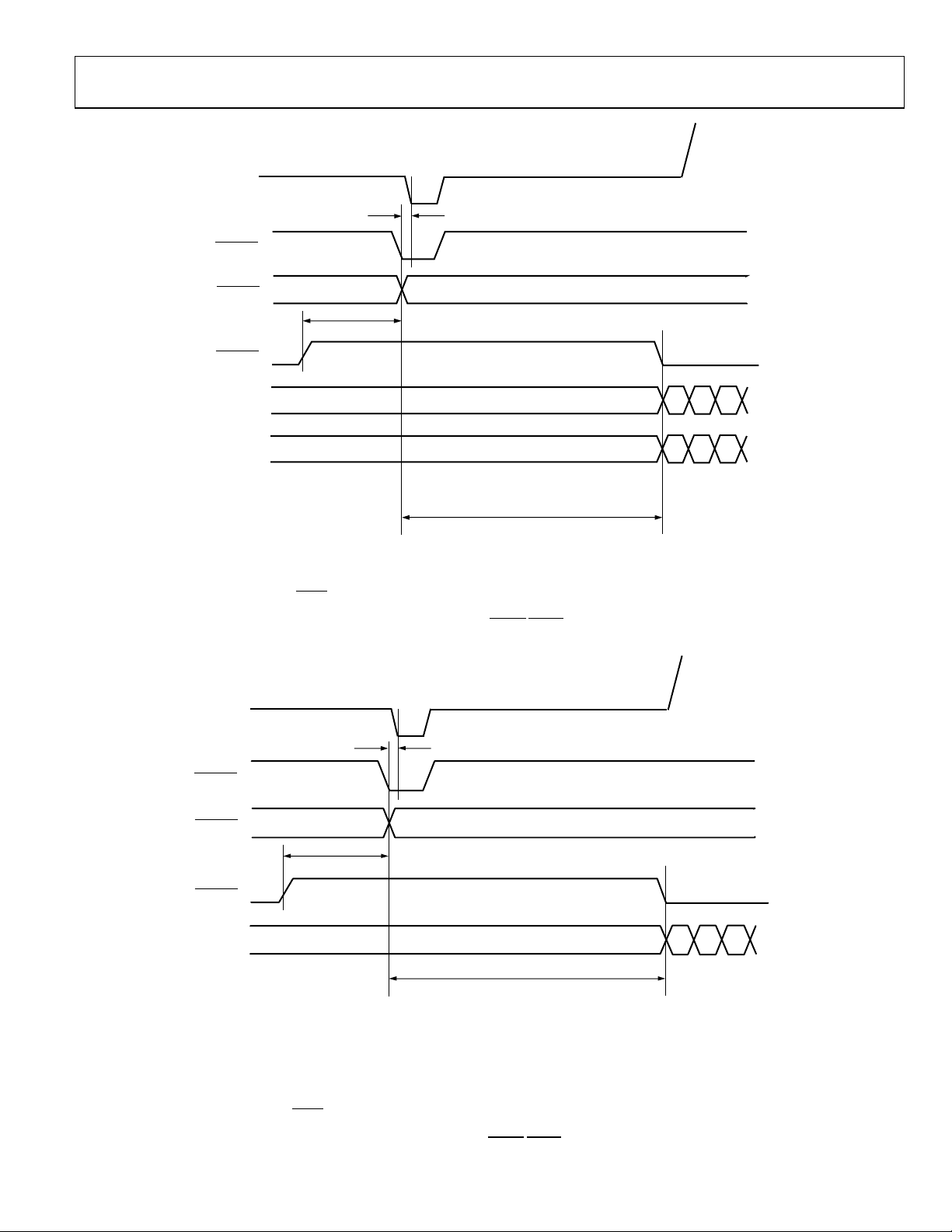
TIMING DIAGRAMS
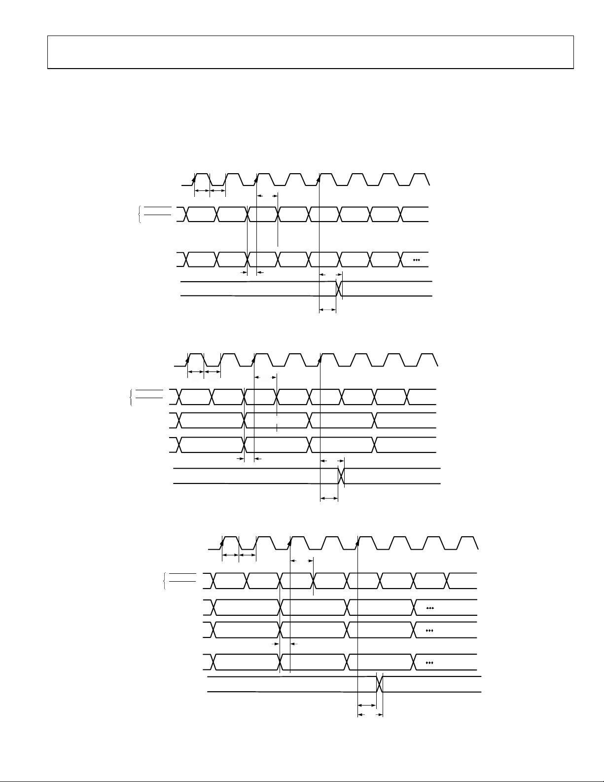
The following abbreviations are used in Figure 2 to Figure 13:
• t
= clock high time
9
• t
= clock low time
10
• t
= data setup time
11
• t
= data hold time
12
• t
= control output access time
13
• t
= control output hold time
14
In addition, refer to Tab l e 36 for the ADV7342/ADV7343 input
configuration.
Figure 2. SD Only, 8-Bit, 4:2:2 YCrCb Pixel Input Mode (Input Mode 000)
Figure 3. SD Only, 16-Bit, 4:2:2 YCrCb Pixel Input Mode (Input Mode 000)
Figure 4. SD Only, 24-Bit, 4:4:4 RGB Pixel Input Mode (Input Mode 000)
Rev. | Page 13 of 108
Page 14
ADV7342/ADV7343 Data Sheet
Y0 Y1 Y2 Y3 Y4 Y5Y7 TO Y0
Cr4Cb4Cr2Cb2Cr0Cb0
CONTROL
OUTPUTS
CLKIN_A
P_HSYNC,
P_VSYNC,
CONTROL
INPUTS
P_BLANK
C7 TO C0
t
9
t
10
t
12
t
11
t
14
t
13
06399-005
Y0 Y1 Y2 Y3 Y4 Y5
Cr4Cr3Cr2Cr1Cr0 Cr5
Cb4Cb3Cb2Cb1
Cb0
Cb5
Y7 TO Y0
CONTROL
OUTPUTS
CLKIN_A
P_HSYNC,
P_VSYNC,
CONTROL
INPUTS
P_BLANK
C7 TO C0
S7 TO S0
t9t
10
t
12
t
11
t
14
t
13
06399-006
CLKIN_A
C7 TO C0
G0 G1 G2 G3 G4 G5
B0 B1 B2 B3 B4 B5
R0 R1 R2 R3 R4 R5
Y7 TO Y0
CONTROL
OUTPUTS
S7 TO S0
P_HSYNC,
P_VSYNC,
CONTROL
INPUTS
P_BLANK
t9t
10
t
12
t
11
t
14
t
13
06399-007
D
Figure 5. ED/HD-SDR Only, 16-Bit, 4:2:2 YCrCb Pixel Input Mode (Input Mode 001)
Figure 6. ED/HD-SDR Only, 24-Bit, 4:4:4 YCrCb Pixel Input Mode (Input Mode 001)
Figure 7. ED/HD-SDR Only, 24-Bit, 4:4:4 RGB Pixel Input Mode (Input Mode 001)
Rev. | Page 14 of 108
Page 15
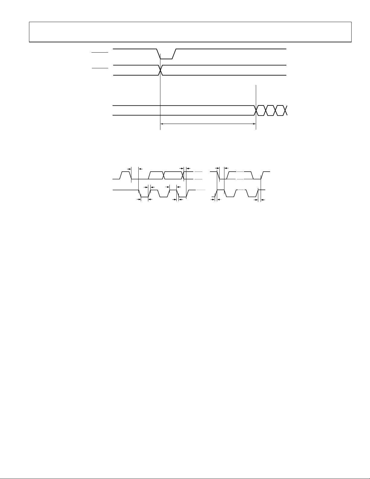
Data Sheet ADV7342/ADV7343
CLKIN_A*
Y7 TO Y0
*LUMA/CHROMA CLOCK RELAT IONSHIP CAN BE INVERTED
USING SUBADDRES S 0x01, BITS 1 AND 2.
CONTRO
L
OU
TPUTS
Cr2Y2Cb2
Y1Cr0Y0Cb0
t
9
t
10
t
12
t
11
t
12
t
11
t
14
t
13
P_HSYNC,
P_VSYNC,
CONTROL
I
NPUTS
P_BLANK
06399-008
Y1Cr0Y0Cb0XY00003FF
*LUMA/CHROM A CLOCK RELATIONSHIP CAN BE INVERTED
USING SUBADDRES S 0x01, BITS 1 AND 2.
CLKIN_A*
Y7 TO Y0
CONTROL
OUTPUTS
t
9
t
10
t
12
t
11
t
12
t
11
t
14
t
13
06399-009
t
9
t
10
t9t
10
t
11
t
11
Y0
Y1
Y2
Y3
Y4
Y5
ED/HD INPUT
SD INPUT
S7 TO S0
CLKIN_A
Y2Cb2Y1Cr0Y0Cb0
Cr4Cb4Cr2Cb2Cr0Cb0
Cr2
Y6
Cb6C7 TO C0
Y7 TO Y0
CLKIN_B
P_HSYNC,
P_VSYNC,
CONTROL
INPUTS
P_BLANK
S_HSYNC,
S_VSYNC
CONTROL
INPUTS
t
12
t
12
06399-010
D
Figure 8. ED/HD-DDR Only, 8-Bit, 4:2:2 YCrCb (
HSYNC/VSYNC
) Pixel Input Mode (Input Mode 010)
Figure 10. SD and ED/HD-SDR, 16-Bit, 4:2:2 ED/HD and 8-Bit, SD Pixel Input Mode (Input Mode 011)
Figure 9. ED/HD-DDR Only, 8-Bit, 4:2:2 YCrCb (EAV/SAV) Pixel Input Mode (Input Mode 010)
Rev. | Page 15 of 108
Page 16
ADV7342/ADV7343 Data Sheet
Cr2
Cr2
Y2Y1Cr0
EH/HD INPUT
SD INPUT
Cb2Y1Cr0
S7 TO S0
CLKIN_A
Y7 TO Y0
CLKIN_B
P_HSYNC,
P_VSYNC,
CONTROL
INPUTS
P_BLANK
S_HSYNC,
S_VSYNC
CONTROL
INPUTS
t9t
10
t9t
10
t
12
t
11
t
12
t
11
t
12
t
11
Y0
Cb0
Cb2
Cb0 Y0 Y2
06399-011
CLKIN_A
Y7 TO Y0
CONTROL
OUTPUTS
Y1Cr0Y0Cb0 Cr2
Y2
Cb2
P_HSYNC,
P_VSYNC,
CONTROL
INPUTS
P_BLANK
t
9t10
t
12
t
11
t
13
t
14
06399-012
t
9
t
11
t
10
t
12
t
13
t
14
CLKIN_A
Y7 TO Y0
CONTROL
OUTPUTS
3FF 00 00 XY Cb0 Y0 Cr0 Y1
06399-013
D
Figure 11. SD and ED/HD-DDR, 8-Bit, 4:2:2 ED/HD and 8-Bit, SD Pixel Input Mode (Input Mode 100)
Figure 12. ED Only (at 54 MHz), 8-Bit, 4:2:2 YCrCb (
HSYNC/VSYNC
) Pixel Input Mode (Input Mode 111)
Figure 13. ED Only (at 54 MHz), 8-Bit, 4:2:2 YCrCb (EAV/SAV) Pixel Input Mode (Input Mode 111)
Rev. | Page 16 of 108
Page 17
Data Sheet ADV7342/ADV7343
Y0 Y1
Y2 Y3
b
a
Cr2Cb2Cr0Cb
0
c
Y OUTPUT
P_HSYNC
P_VSYNC
P_BLANK
Y7 TO Y0
C7 TO C0
a AND b AS PER REL E V ANT STANDARD.
c = PIPELINE DELAY. PLEASE REFER TO RELEVANT PIPELINE DELAY. THIS CAN BE FOUND IN THE DIGITAL TIMING
SPECIFICATION SECTION OF THE DATA SHEET.
A FALLING EDGE OF HSYNC INTO THE ENCODER GENERATES A SYNC FALLING EDGE ON THE OUTPUT AFTER A TIME
EQUAL TO THE PIPELINE DELAY.
06399-014
Y7 TO Y0
Cb0 Y0
Cr0 Y1
b
a
a = 32 CLOCK CYCLE S FOR 525p
a = 24 CLOCK CYCLE S FOR 625p
AS RECOMMENDE D B
Y STANDARD
b(MIN) = 244 CLOCK CYCLES FOR 525p
b(MIN) = 264 CLOCK CYCLES FOR 625p
P_HSYNC
P_VSYNC
P_BLANK
c
Y OUTPUT
c = PIPELINE DELAY. PLEASE REFER TO RELEVANT PIPELINE DELAY. THIS CAN BE FOUND I N THE DIGITAL TIMING
SPECIFICATION SECTION OF THE DATA SHEET.
A FALLING ED
GE OF HSYNC INTO THE ENCODE R GENERATES A SYNCFALLING EDGE ON THE OUTPUTAFTER A TIME
EQUAL TO THE PIPELINE DELAY.
06399-015
D
Figure 14. ED-SDR, 16-Bit, 4:2:2 YCrCb (
HSYNC/VSYNC
) Input Timing Diagram
Figure 15. ED-DDR, 8-Bit, 4:2:2 YCrCb (
HSYNC/VSYNC
Rev. | Page 17 of 108
) Input Timing Diagram
Page 18
ADV7342/ADV7343 Data Sheet
Y0 Y1
Y2 Y3
b
a
Cr2Cb2Cr0Cb
0
c
Y OUTPUT
P_HSYNC
P_VSYNC
P_BLANK
Y7 TO Y0
C7 TO C0
a AND b AS PER REL E V ANT STANDARD.
c = PIPELINE DELAY. PLEASE REFER TO RELEVANT PIPELINE DELAY. THIS CAN BE FOUND IN THE DIGITAL TIMING
SPECIFICATION SECTION OF THE DATA SHEET.
A FALLING EDGE OF HSYNC INTO THE ENCODER GENERATES A FALLING EDGE OF TRI-LEVEL SYNC ON THE OUTPUT
AFTER A TIME EQUAL TO THE PIPELINE DELAY.
06399-016
Y7 TO Y0
Cb0 Y0
Cr0 Y1
b
a
P_HSYNC
P_VSYNC
P_BLANK
c
Y OUTPUT
a AND b AS PER REL E V ANT STANDARD.
c = PIPELINE DELAY. PLEASE REFER TO RELEVANT PIPELINE DELAY. THIS CAN BE FOUND IN THE DIGITAL TIMING
SPECIFICATION SECTION OF THE DATA SHEET.
A FALLING EDGE OF HSYNC INTO THE ENCODER GENERATES A FALLING EDGE OF TRI-LEVEL SYNC ON THE OUTPUT
AFTER A TIME EQUAL TO THE PIPELINE DELAY.
06399-017
D
Figure 16. HD-SDR, 16-Bit, 4:2:2 YCrCb (
HSYNC/VSYNC
) Input Timing Diagram
Figure 17. HD-DDR, 8-Bit, 4:2:2 YCrCb (
HSYNC/VSYNC
) Input Timing Diagram
Rev. | Page 18 of 108
Page 19
Data Sheet ADV7342/ADV7343
Cb Y
Cr Y
PAL = 264 CLOCK CY CLES
NTSC = 244 CLOCK CY CLES
Y7 TO Y0*
S_VSYNC
S_HSYNC
*SELECTE D BY S UBADDRE S S 0x01, BIT 7.
06399-018
t
3
t
3
t
4
t
7
t
8
t
5
SDA
SCL
t
1
t
2
t
6
06399-019
D
Figure 18. SD Input Timing Diagram (Timing Mode 1)
Figure 19. MPU Port Timing Diagram (I
2
C Mode)
Rev. | Page 19 of 108
Page 20
ADV7342/ADV7343 Data Sheet
D
ABSOLUTE MAXIMUM RATINGS
Table 13.
Parameter1 Rating
VAA to AGND −0.3 V to +3.9 V
VDD to DGND −0.3 V to +2.3 V
PVDD to PGND −0.3 V to +2.3 V
V
to GND_IO −0.3 V to +3.9 V
DD_IO
AGND to DGND −0.3 V to +0.3 V
AGND to PGND −0.3 V to +0.3 V
AGND to GND_IO −0.3 V to +0.3 V
DGND to PGND −0.3 V to +0.3 V
DGND to GND_IO −0.3 V to +0.3 V
PGND to GND_IO −0.3 V to +0.3 V
Digital Input Voltage to GND_IO −0.3 V to V
DD_IO
+ 0.3 V
Analog Outputs to AGND −0.3 V to VAA
Maximum CLKIN Input Frequency 80 MHz
Storage Temperature Range (TS) −65°C to +150°C
Junction Temperature (TJ) 150°C
Lead Temperature (Soldering, 10 sec) 260°C
1
Analog output short circuit to any power supply or common can be of an
indefinite duration.
Stresses above those listed under Absolute Maximum Ratings
may cause permanent damage to the device. This is a stress
rating only; functional operation of the device at these or any
other conditions above those indicated in the operational
section of this specification is not implied. Exposure to absolute
maximum rating conditions for extended periods may affect
device reliability.
The ADV7342/ADV7343 are high performance integrated
circuits with an ESD rating of <1 kV, and they are ESD sensitive.
Proper precautions should be taken for handling and assembly.
THERMAL RESISTANCE
θJA is specified for the worst-case conditions, that is, a device
soldered in a circuit board for surface-mount packages.
Table 14. Thermal Resistance
Package Type θJA θ
1
Unit
JC
64-Lead LQFP 47 11 °C/W
1
Values are based on a JEDEC 4-layer test board.
The ADV7342/ADV7343 are RoHS-compliant, Pb-free products.
The lead finish is 100% pure Sn electroplate. The devices are
suitable for Pb-free applications up to 255°C (±5°C) IR reflow
(JEDEC STD-20).
They are backward compatible with conventional SnPb soldering
processes. The electroplated Sn coating can be soldered with
Sn/Pb solder paste at conventional reflow temperatures of
220°C to 235°C.
ESD CAUTION
Rev. | Page 20 of 108
Page 21
Data Sheet ADV7342/ADV7343
S_HSYNC49S_VSYNC
V
Y5
10
V
DD
12
Y6
13
Y7
14
TEST2
15
TEST3
16
C0
11
DGND
17C118C219
ALSB
20
SDA
21
SCL
22 23
P_HSYNC
24
P_VSYNC
25
P_BLANK
26
C4
C327C528C629C7
30
CLKIN_A
31 32
PGND
PIN 1
ADV7342/ADV7343
TOP VIEW
(Not to S cale)
EXT_LF2
06399-021
30
CLKIN_A
I
Pixel Clock Input for HD Only (74.25 MHz), ED1 Only (27 MHz or 54 MHz), or SD Only (27 MHz).
D
PIN CONFIGURATION AND FUNCTION DESCRIPTIONS
TEST0
TEST1
Table 15. Pin Function Descriptions
Input/
Pin No. Mnemonic
13, 12,
Y7 to Y0 I 8-Bit Pixel Port. Y0 is the LSB. Refer to Table 36 for input modes.
Output Description
9 to 4
29 to 25,
C7 to C0 I 8-Bit Pixel Port. C0 is the LSB. Refer to Table 36 for input modes.
18 to 16
62 to 58,
S7 to S0 I 8-Bit Pixel Port. S0 is the LSB. Refer to Table 36 for input modes.
55 to 53
52, 51, 15,
14, 3, 2
TEST5 to
TEST0
I Unused. These pins should be connected to DGND.
DD_IO
GND_IO63CLKIN_B62S761S660S559S458S357DGND56V
64
1
2
3
4
Y0
5
Y1
6
Y2
7
Y3
8
Y4
9
DD
55S254S153S052
TEST551TEST4
50
48
SFL
47
R
SET1
46
V
REF
45
COMP1
44
DAC 1
43
DAC 2
42
DAC 3
41
V
AA
40
AGND
39
DAC 4
38
DAC 5
37
DAC 6
36
R
SET2
35
COMP2
34
PV
DD
33
EXT_LF1
Figure 20. Pin Configuration
63 CLKIN_B I
Pixel Clock Input for Dual Modes Only. Requires a 27 MHz reference clock for ED operation or a
74.25 MHz reference clock for HD operation.
50
S_HSYNC
I/O
SD Horizontal Synchronization Signal. This pin can also be configured to output an SD, ED, or HD
horizontal synchronization signal. See the External Horizontal and Vertical Synchronization
Control section.
49
S_VSYNC
I/O
SD Vertical Synchronization Signal. This pin can also be configured to output an SD, ED, or HD
vertical synchronization signal. See the External Horizontal and Vertical Synchronization Control
22
P_HSYNC
I
section.
ED/HD Horizontal Synchronization Signal. See the External Horizontal and Vertical
Synchronization Control section.
23
P_VSYNC
I
ED/HD Vertical Synchronization Signal. See the External Horizontal and Vertical Synchronization
Control section.
24
48 SFL I/O
47 R
P_BLANK
I
SET1
I ED/HD Blanking Signal. See the External Horizontal and Vertical Synchronization Control section.
Subcarrier Frequency Lock (SFL) Input. The SFL input is used to drive the color subcarrier DDS
system.
This pin is used to control the amplitudes of the DAC 1, DAC 2, and DAC 3 outputs. For full-drive
operation (for example, into a 37.5 Ω load), a 510 Ω resistor must be connected from R
AGND. For low-drive operation (for example, into a 300 Ω load), a 4.12 kΩ resistor must be
connected from R
to AGND.
SET1
Rev. | Page 21 of 108
SET1
to
Page 22

ADV7342/ADV7343 Data Sheet
20
SDA
I/O
I2C Data Input/Output.
D
36 R
45, 35
44, 43, 42
39, 38, 37
21 SCL I I2C Clock Input.
I
SET2
COMP1,
COMP2
DAC 1, DAC 2,
DAC 3
DAC 4, DAC 5,
DAC 6
This pin is used to control the amplitudes of the DAC 4, DAC 5, and DAC 6 outputs. A 4.12 kΩ
resistor must be connected from R
to AGND.
SET2
O Compensation Pins. Connect a 2.2 nF capacitor from both COMP pins to V
O DAC Outputs. Full- and low-drive capable DACs.
O DAC Outputs. Low-drive only capable DACs.
.
AA
19 ALSB I
This signal sets up the LSB
2
of the MPU I2C address (see the Power Supply Sequencing section for
more information).
46 V
Optional External Voltage Reference Input for DACs or Voltage Reference Output.
REF
41 VAA P Analog Power Supply (3.3 V).
10, 56 VDD P
Digital Power Supply (1.8 V). For dual-supply configurations, V
can be connected to other 1.8 V
DD
supplies through a ferrite bead or suitable filtering.
1 V
34 PVDD P
P Input/Output Digital Power Supply (1.8 V or 3.3 V).
DD_IO
PLL Power Supply (1.8 V). For dual-supply configurations, PV
can be connected to other 1.8 V
DD
supplies through a ferrite bead or suitable filtering.
33 EXT_LF1 I External Loop Filter for On-Chip PLL 1.
31 EXT_LF2 I External Loop Filter for On-Chip PLL 2.
32 PGND G PLL Ground Pin.
40 AGND G Analog Ground Pin.
11, 57 DGND G Digital Ground Pin.
64 GND_IO G Input/Output Supply Ground Pin.
1
ED = enhanced definition = 525p and 625p.
2
LSB = least significant bit. In the ADV7342, setting the LSB to 0 sets the I2C address to 0xD4. Setting it to 1 sets the I2C address to 0xD6. In the ADV7343, setting the
LSB to 0 sets the I
2
C address to 0x54. Setting it to 1 sets the I2C address to 0x56.
Rev. | Page 22 of 108
Page 23
Data Sheet ADV7342/ADV7343
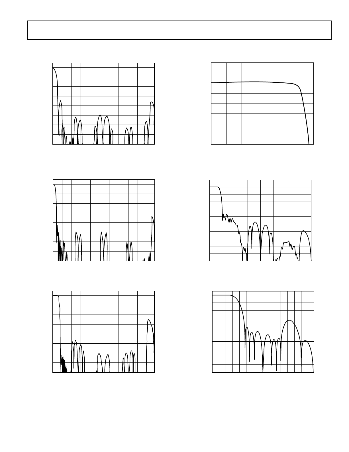
FREQUENCY (MHz)
EDPr/Pb RESPONSE. LINEAR INTERP FROM 4:2:2 TO 4:4:4
0
GAIN (dB)
–70
–60
–50
–40
–30
–20
–10
–80
20020 40 60 80 100 120 140 160 1800
06399-022
FREQUENCY (MHz)
EDPr/Pb RESPONSE. SSAF INTERP FROM 4:2:2 TO 4:4:4
0
GAIN (dB)
–70
–60
–50
–40
–30
–20
–10
–80
20020 40 60 80 100 120 140 160 1800
06399-023
FREQUENCY (MHz)
Y RESPONSE IN ED 8× OVERSAMPLING MODE
0
GAIN (dB)
–70
–60
–50
–40
–30
–20
–10
–80
20020 40 60 80 100 120 140 160 1800
06399-024
FREQUENCY (MHz)
Y RESPONSE IN ED 8× OVERSAMPLING MODE
GAIN (dB)
–2.5
–2.0
–1.5
–1.0
–0.5
0
0.5
1.0
–3.0
122 4 6 8 100
06399-025
FREQUENCY (MHz)
HD Pr/Pb RESPONSE. SSAF INTERP FROM 4:2:2 TO 4:4:4
10
0
GAIN (dB)
–70
–60
–50
–40
–30
–20
–10
–100
–80
–90
148.018.5 37.
0 55.5 74.0 92.5 111.0 129.50
06399-026
HD Pr/Pb RES P ONSE. 4:4:4 I NP UT MODE
GAIN (dB)
FREQUENCY (MHz)
0
–10
–20
–30
–40
–50
–60
–70
–80
–90
–100
10 20
30 40 50 60 70 80 90 100 110 120 130 140
06399-027
D
TYPICAL PERFORMANCE CHARACTERISTICS
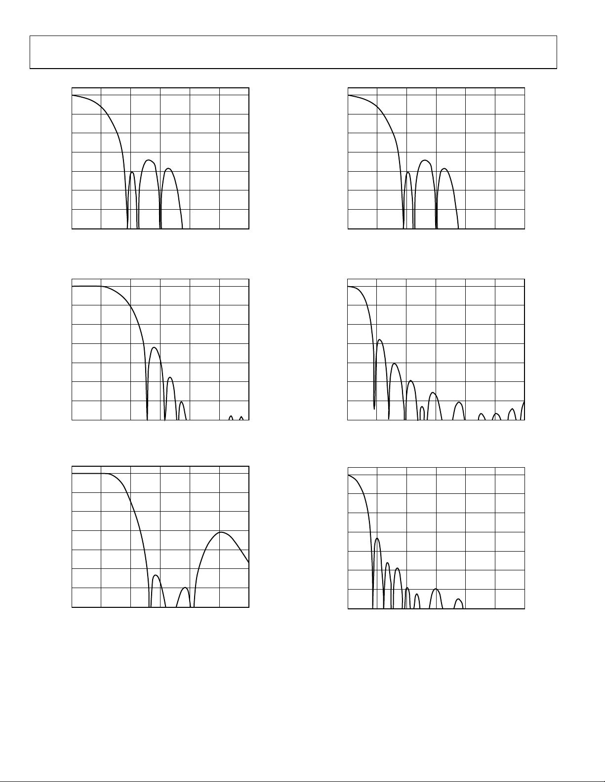
Figure 21. ED 8× Oversampling, PrPb Filter (Linear) Response
Figure 22. ED 8× Oversampling, PrPb Filter (SSAF™) Response
Figure 24. ED 8× Oversampling, Y Filter Response (Focus on Pass Band)
Figure 25. HD 4× Oversampling, PrPb (SSAF) Filter Response (4:2:2 Input)
Figure 23. ED 8× Oversampling, Y Filter Response
Figure 26. HD 4× Oversampling, PrPb (SSAF) Filter Response (4:4:4 Input)
Rev. | Page 23 of 108
Page 24
ADV7342/ADV7343 Data Sheet
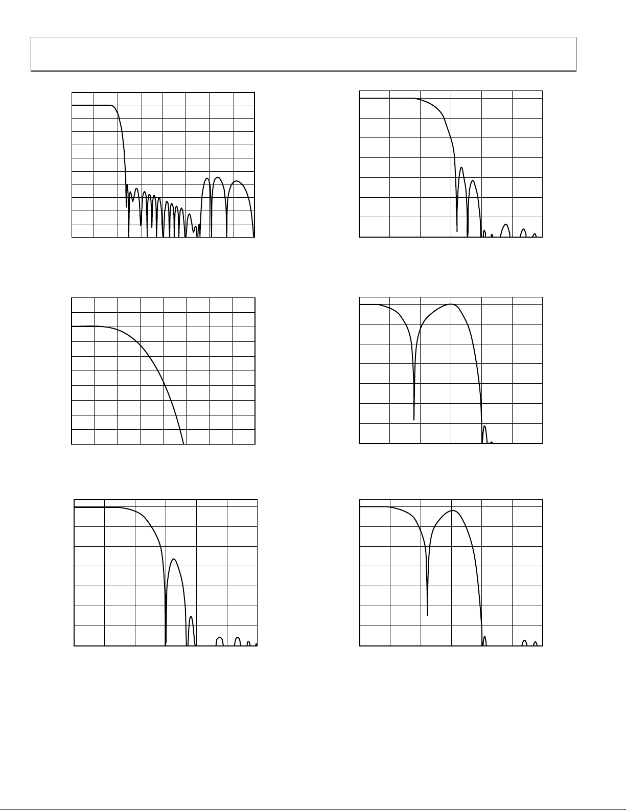
FREQUENCY (MHz)
Y RESPONSE IN HD 4× OVERSAMPLING MODE
10
0
GAIN (dB)
–70
–60
–50
–40
–30
–20
–10
–100
–80
–90
148.018.5 37.0 55.5 74.0 92.5 111.0 129.50
06399-028
Y PASS BAND IN HD 4x O V E RS AM P LING MODE
3.0
–12.0
27.750 46.250
FREQUENCY (MHz)
GAIN (dB)
1.5
0
–1.5
–3.0
–4.5
–6.0
–7.5
–9.0
–10.
5
30.063 32.375 34.688 37.000 39.312 41.625 43.937
06399-029
FREQUENCY (MHz)
MAGNITUDE ( dB)
0
121086420
–10
–30
–50
–60
–70
–20
–40
06399-030
FREQUENCY (MHz)
MAGNITUDE ( dB)
0
121086420
–10
–30
–50
–60
–70
–20
–40
06399-031
FREQUENCY (MHz)
MAGNITUDE ( dB)
0
121086420
–10
–30
–50
–60
–70
–20
–40
06399-032
FREQUENCY (MHz)
MAGNITUDE ( dB)
0
121086420
–10
–30
–50
–60
–70
–20
–40
06399-033
D
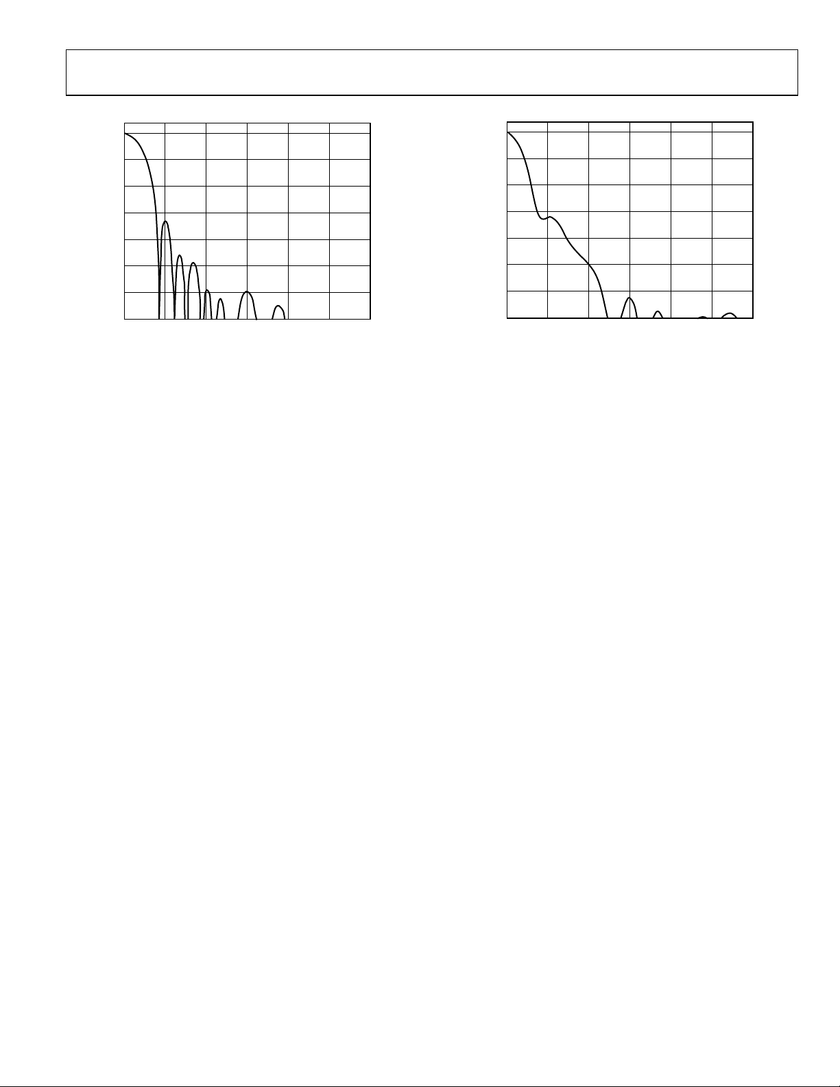
Figure 27. HD 4× Oversampling, Y Filter Response
Figure 28. HD 4× Oversampling, Y Filter Response (Focus on Pass Band)
Figure 30. SD PAL, Luma Low-Pass Filter Response
Figure 31. SD NTSC, Luma Notch Filter Response
Figure 29. SD NTSC, Luma Low-Pass Filter Response
Figure 32. SD PAL, Luma Notch Filter Response
Rev. | Page 24 of 108
Page 25
Data Sheet ADV7342/ADV7343
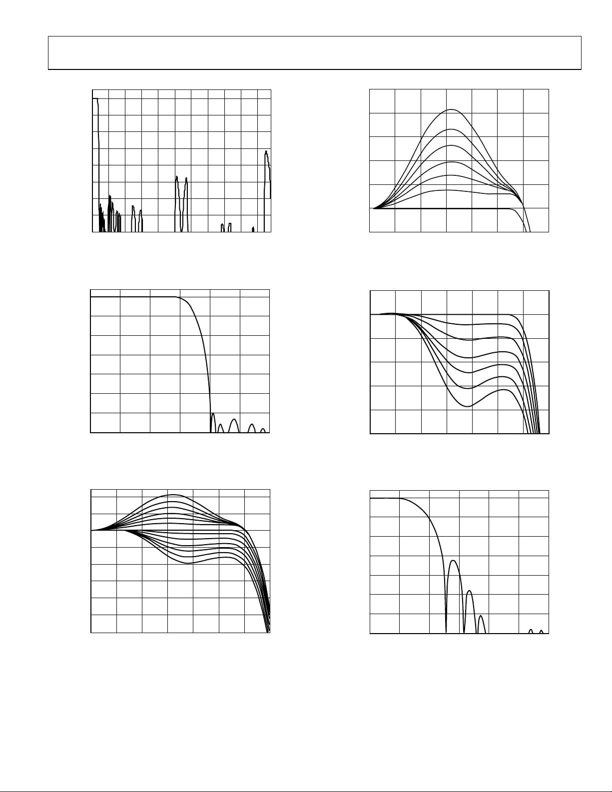
FREQUENCY (MHz)
Y RESPO NSE I N SD O VER SAMPL I N G MO DE
GAIN (dB)
0
–50
–80
0 20 40 60 80 100 120 140 160 180 200
–10
–40
–60
–70
–20
–30
06399-034
FREQUENCY (MHz)
MAGNITUDE ( dB)
0
121086420
–10
–30
–50
–60
–70
–20
–40
06399-035
FREQUENCY (MHz)
4
7
MAGNITUDE ( dB)
2
–2
–6
–8
–12
0
–4
5
–10
6
0
1
2
3
4
06399-036
FREQUENCY (MHz)
7
MAGNITUDE ( dB)
5
4
2
1
–1
3
5
0
6
0
1
2
3
4
06399-037
FREQUENCY (MHz)
7
MAGNITUDE ( dB)
1
0
–2
–3
–5
–1
5
–4
6
0
1
2
3
4
06399-038
FREQUENCY (MHz)
0
12
MAGNITUDE ( dB)
–10
–30
–50
–60
–70
–20
–40
10
8
4
620
06399-039
D
Figure 33. SD, 16× Oversampling, Y Filter Response
Figure 34. SD Luma SSAF Filter Response up to 12 MHz
Figure 36. SD Luma SSAF Filter, Programmable Gain
Figure 37. SD Luma SSAF Filter, Programmable Attenuation
Figure 35. SD Luma SSAF Filter, Programmable Responses
Figure 38. SD Luma CIF Low-Pass Filter Response
Rev. | Page 25 of 108
Page 26
ADV7342/ADV7343 Data Sheet
FREQUENCY (MHz)
0
12
MAGNITUDE ( dB)
–10
–30
–50
–60
–70
–20
–40
10
8
4
620
06399-040
FREQUENCY (MHz)
0
12
MAGNITUDE ( dB)
–10
–30
–50
–60
–70
–20
–40
10
8
4
620
06399-041
FREQUENCY (MHz)
0
12
MAGNITUDE ( dB)
–10
–30
–50
–60
–70
–20
–40
10
8
4
620
06399-042
FREQUENCY (MHz)
0
12
MAGNITUDE ( dB)
–10
–30
–50
–60
–70
–20
–40
10
8
4
620
06399-043
FREQUENCY (MHz)
0
12
MAGNITUDE ( dB)
–10
–30
–50
–60
–70
–20
–40
10
8
4
620
06399-044
FREQUENCY (MHz)
0
12
MAGNITUDE ( dB)
–10
–30
–50
–60
–70
–20
–40
10
8
4
620
06399-045
D
Figure 39. SD Luma QCIF Low-Pass Filter Response
Figure 40. SD Chroma 3.0 MHz Low-Pass Filter Response
Figure 42. SD Chroma 1.3 MHz Low-Pass Filter Response
Figure 43. SD Chroma 1.0 MHz Low-Pass Filter Response
Figure 41. SD Chroma 2.0 MHz Low-Pass Filter Response
Figure 44. SD Chroma 0.65 MHz Low-Pass Filter Response
Rev. | Page 26 of 108
Page 27
Data Sheet ADV7342/ADV7343
FREQUENCY (MHz)
0
12
MAGNITUDE ( dB)
–10
–30
–50
–60
–70
–20
–40
10
8
4
620
06399-046
FREQUENCY (MHz)
0
12
MAGNITUDE ( dB)
–10
–30
–50
–60
–70
–20
–40
10
8
4
620
06399-047
D
Figure 45. SD Chroma CIF Low-Pass Filter Response
Figure 46. SD Chroma QCIF Low-Pass Filter Response
Rev. | Page 27 of 108
Page 28
1
Read
0xD7
1
Write
0x56
1 1 0
1 0 1
A1 X
ADDRESS
CONTROL
SET UP BY
ALSB
READ/WRITE
CONTROL
0 WRITE
1 READ
06399-048
0
1
0 1
0 1
A1 X
READ/WRITE
CONTROL
0 WRITE
1 READ
06399-145
ADDRESS
CONTROL
SET UP BY
ALSB
D
ADV7342/ADV7343 Data Sheet
MPU PORT DESCRIPTION
Devices such as a microprocessor can communicate with the
ADV7342/ADV7343 through a 2-wire serial (I
2
C-compatible)
bus. After power-up or reset, the MPU port is configured for
2
I
C operation.
I2C OPERATION
The ADV7342/ADV7343 support a 2-wire serial (I2C-compatible)
microprocessor bus driving multiple peripherals. This port
operates in an open-drain configuration. Two wires, serial data
(SDA) and serial clock (SCL), carry information between any
device connected to the bus and the ADV7342/ADV7343. The
slave address of the device depends on the device (ADV7342 or
ADV7343), the operation (read or write), and the state of the
ALSB pin (0 or 1). See Ta b le 16, Figure 47, and Figure 48. The
LSB sets either a read or a write operation. Logic 1 corresponds
to a read operation, and Logic 0 corresponds to a write
operation. A1 is controlled by setting the ALSB pin of the
ADV7342/ ADV7343 to Logic 0 or Logic 1.
Table 16. ADV7342/ADV7343 I
Device ALSB Operation Slave Address
ADV7342 0 Write 0xD4
0 Read 0xD5
1 Write 0xD6
ADV7343 0 Write 0x54
0 Read 0x55
1 Read 0x57
Figure 47. ADV7342 I
Figure 48. ADV7343 I
Analog Devices, Inc., recommends tying up ALSB. If this is not
done, a power supply sequence (PSS) may be required. For more
information on the PSS, see the Power Supply Sequencing section.
The various devices on the bus use the following protocol. The
2
C Slave Addresses
2
C Slave Address
2
C Slave Address
Rev. | Page 28 of 108
master initiates a data transfer by establishing a start condition,
defined by a high-to-low transition on SDA while SCL remains
high. This indicates that an address/data stream follows. All
peripherals respond to the start condition and shift the next
eight bits (7-bit address plus the R/
W
bit). The bits are
transferred from MSB down to LSB. The peripheral that
recognizes the transmitted address responds by pulling the data
line low during the ninth clock pulse. This is known as an
acknowledge bit. All other devices withdraw from the bus at
this point and maintain an idle condition. The idle condition
occurs when the device monitors the SDA and SCL lines
waiting for the start condition and the correct transmitted
address. The R/
W
bit determines the direction of the data.
Logic 0 on the LSB of the first byte means that the master writes
information to the peripheral. Logic 1 on the LSB of the first byte
means that the master reads information from the peripheral.
The ADV7342/ADV7343 act as a standard slave device on the
bus. The data on the SDA pin is eight bits long, supporting the
7-bit addresses plus the R/
W
bit. It interprets the first byte as
the device address and the second byte as the starting subaddress.
There is a subaddress auto-increment facility. This allows data
to be written to or read from registers in ascending subaddress
sequence starting at any valid subaddress. A data transfer is
always terminated by a stop condition. The user can also access
any unique subaddress register on a one-by-one basis without
updating all the registers.
Stop and start conditions can be detected at any stage during the
data transfer. If these conditions are asserted out of sequence with
normal read and write operations, they cause an immediate jump
to the idle condition. During a given SCL high period, the user
should issue only a start condition, a stop condition, or a stop
condition followed by a start condition. If an invalid subaddress
is issued by the user, the ADV7342/ADV7343 do not issue an
acknowledge but return to the idle condition. If the user uses the
auto-increment method of addressing the encoder and exceeds
the highest subaddress, the following actions are taken:
• In read mode, the highest subaddress register contents are
output until the master device issues a no acknowledge.
This indicates the end of a read. A no acknowledge condition
occurs when the SDA line is not pulled low on the ninth pulse.
• In write mode, the data for the invalid byte is not loaded
into any subaddress register, a no acknowledge is issued by
the ADV7342/ADV7343, and the parts return to the idle
condition.
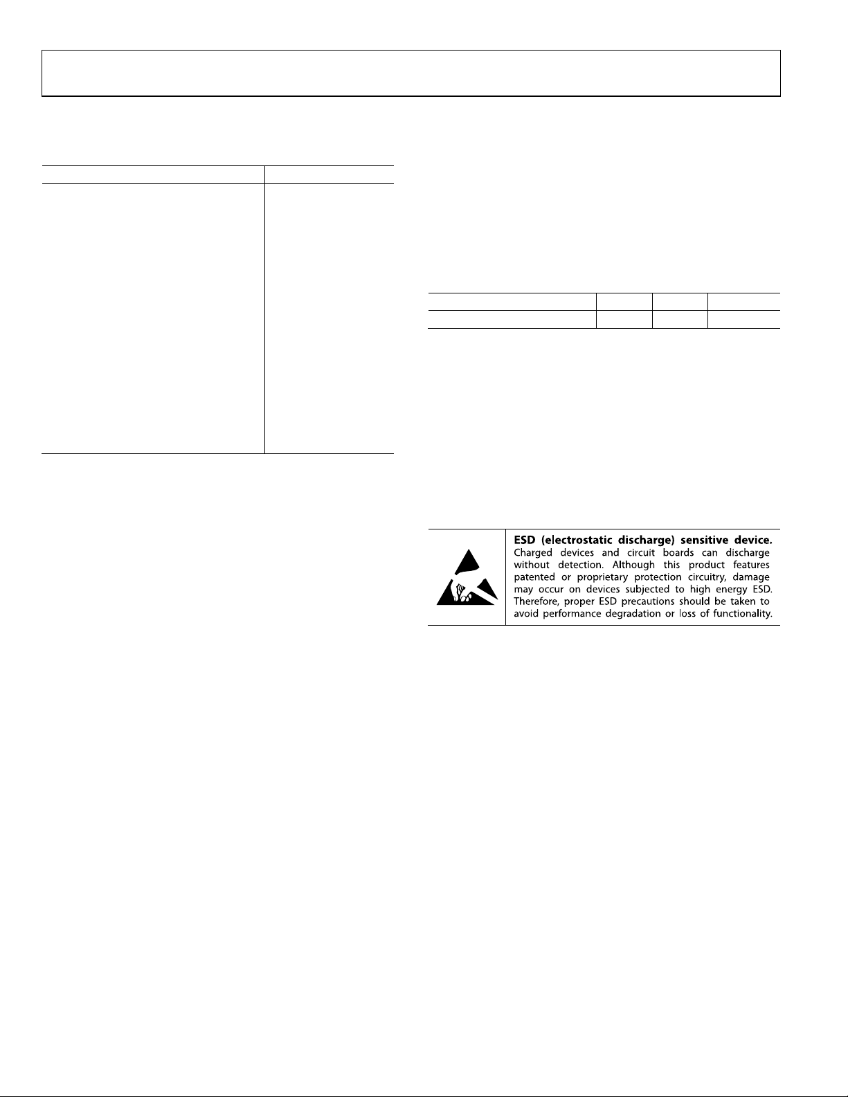
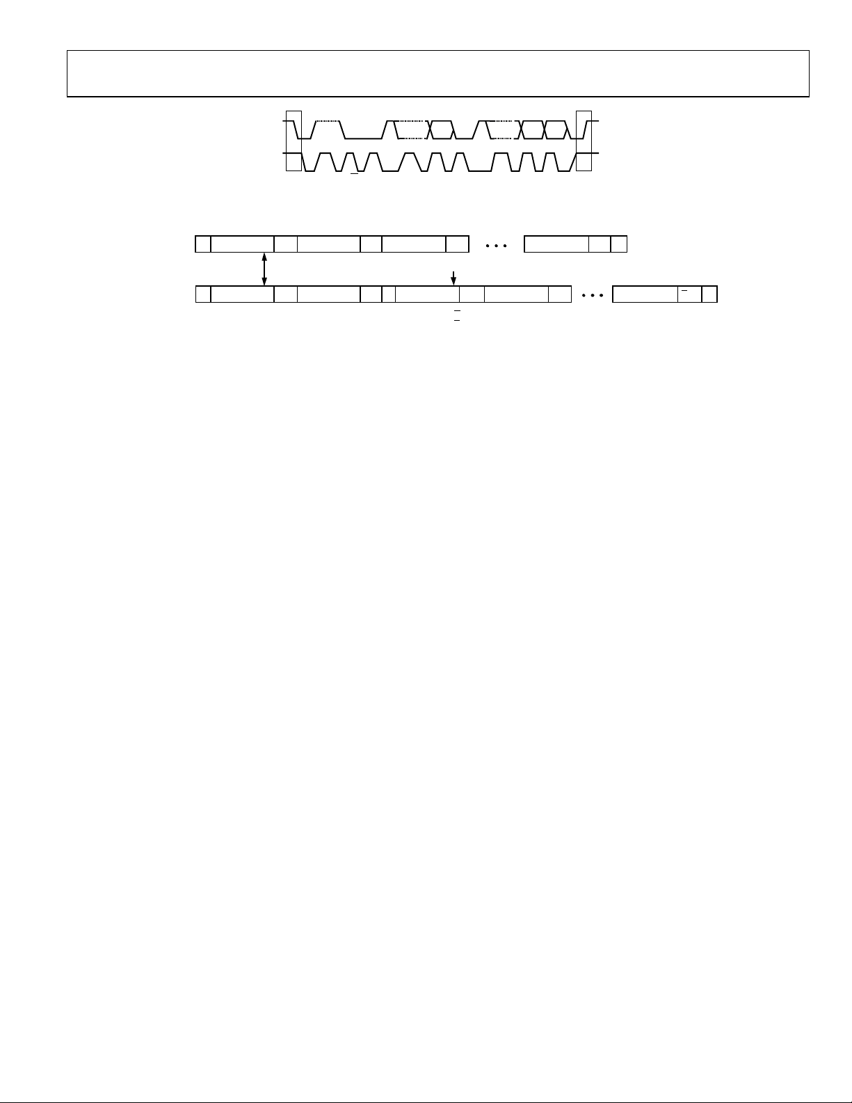
Figure 49 shows data transfer for a write sequence and the start
and stop conditions. Figure 50 shows bus write and read
sequences.
Page 29
Data Sheet ADV7342/ADV7343
SDA
SCL
START ADDR R/W ACK SUBADDRESS ACK DATA ACK STOP
1–7 8
9S1–7
1–7
P
8
9
8
9
06399-049
WRITE
SEQUENCE
READ
SEQUENCE
S SLAVE ADDR A(S) SUBADDR A(S) DATA DATA A(S) P
S SLAVE ADDR A(S) SUBADDR A(S) S SLAVE ADDR A(S) DATA DATAA(M) A(M) P
S = START BIT
P = STOP BIT
A(S) = ACKNOWLEDG E B Y SLAVE
A(M) = ACKNOWLEDG E B Y MASTER
A(S) = NO-ACKNOWLE DGE BY SLAVE
A(M) = NO-ACKNOWLE DGE BY MASTER
LSB = 0
LSB = 1
A(S)
06399-050
D
Figure 49. I
2
C Data Transfer
Figure 50. I
2
C Read and Write Sequence
Rev. | Page 29 of 108
Page 30
ADV7342/ADV7343 Data Sheet
D
REGISTER MAP ACCESS
A microprocessor can read from or write to all registers of the
ADV7342/ADV7343 via the MPU port, except for registers that
are specified as read-only or write-only registers.
The subaddress register determines which register the next
read or write operation accesses. All communication through
the MPU port starts with an access to the subaddress register.
A read/write operation is then performed from/to the target
address, which increments to the next address until the
transaction is complete.
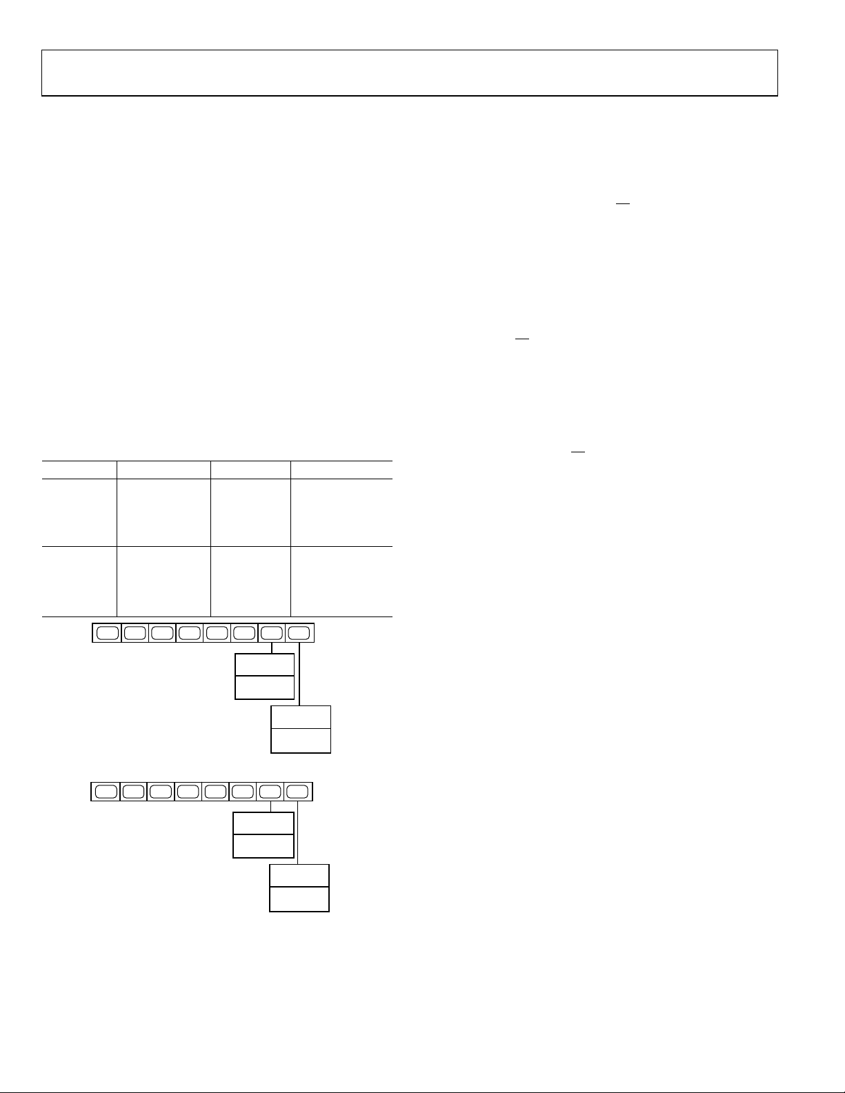
Table 17. Register 0x00
SR7 to Bit Number Register Reset
SR0 Register Bit Description 7 6 5 4 3 2 1 0 Setting Value
0x00 Power
mode
Sleep mode. With this control enabled, the current consumption is
reduced to μA level. All DACs and the internal PLL circuits are
disabled. Registers can be read from and written to in sleep mode.
PLL and oversampling control. This control allows the internal PLL 1
circuit to be powered down and the oversampling to be switched off.
DAC 3: power on/off. 0 DAC 3 off
DAC 2: power on/off. 0 DAC 2 off
DAC 1: power on/off. 0 DAC 1 off
DAC 6: power on/off. 0 DAC 6 off
DAC 5: power on/off. 0 DAC 5 off
DAC 4: power on/off. 0 DAC 4 off
REGISTER PROGRAMMING
Table 17 to Table 35 describe the functionality of each register.
All registers can be read from as well as written to, unless
otherwise stated.
SUBADDRESS REGISTER (SR7 TO SR0)
The subaddress register is an 8-bit write-only register. After the
MPU port is accessed and a read/write operation is selected, the
subaddress is set up. The subaddress register determines to or
from which register the operation takes place.
0 Sleep
mode off
1 Sleep
mode on
0 PLL 1 on
1 PLL 1 off
1 DAC 3 on
1 DAC 2 on
1 DAC 1 on
1 DAC 6 on
1 DAC 5 on
1 DAC 4 on
0x12
Table 18. Register 0x01 to Register 0x09
SR7 to Bit Number1 Reset
SR0 Register Bit Description 7 6 5 4 3 2 1 0 Register Setting Value
0x01 Mode select Reserved. 0 0x00
DDR clock edge alignment
(only used for EDHD-DDR modes)
Reserved. 0
Input mode (see Register
0x30, Bits[7:3] for ED/HD
standard selection)
Y/C/S bus swap 0 Allows data to be applied to data ports in
2
and
0 0 Chroma clocked in on rising clock edge; luma
0 1 Reserved
1 0 Reserved
1 1 Luma clocked in on rising clock edge;
0 0 0 SD input only
0 0 1 ED/HD-SDR input only
0 1 0 ED/HD-DDR input only
0 1 1 SD and ED/HD-SDR
1 0 0 SD and ED/HD-DDR
1 0 1 Reserved
1 1 0 Reserved
1 1 1 ED only (at 54 MHz)
1
Rev. | Page 30 of 108
clocked in on falling clock edge
chroma clocked in on falling clock edge
various configurations (SD feature only)
Page 31

Data Sheet ADV7342/ADV7343
D
SR7 to Bit Number1 Reset
SR0 Register Bit Description 7 6 5 4 3 2 1 0 Register Setting Value
0x02 Mode
Register 0
0x03 ED/HD CSC
Matrix 0
0x04 ED/HD CSC
Matrix 1
0x05 ED/HD CSC
Matrix 2
0x06 ED/HD CSC
Matrix 3
0x07 ED/HD CSC
Matrix 4
0x08 ED/HD CSC
Matrix 5
0x09 ED/HD CSC
Matrix 6
1
x = Logic 0 or Logic 1.
2
ED = enhanced definition = 525p and 625p.
3
Subaddress 0x31, Bit 2 must also be enabled (ED/HD). Subaddress 0s84, Bit 6 must also be enabled (SD).
Reserved 0 0 must be written to this bit 0x20
HD interlace external
VSYNC and HSYNC
0 Default
1
If using HD
HSYNC/VSYNCinterlace mode,
setting this bit to 1 is recommended (see the
HD Interlace External
P_HSYNC and P_VSYNC
Considerations section for more information)
Test pattern black bar.3 0 Disabled
1 Enabled
Manual CSC matrix adjust 0 Disable manual CSC matrix adjust
1 Enable manual CSC matrix adjust
Sync on RGB 0 No sync
1 Sync on all RGB outputs
RGB/YPrPb output select 0 RGB component outputs
1 YPrPb component outputs
SD sync output enable 0 No sync output
1
Output SD syncs on
HSYNC
and
VSYNC
pins
ED/HD sync output enable 0 No sync output
1
Output ED/HD syncs on
VSYNC
pins
HSYNC
and
x x LSBs for GY 0x03
x x LSBs for RV 0xF0
x x LSBs for BU
x x LSBs for GV
x x LSBs for GU
x x x x x x x x Bits[9:2 ] for GY 0x4E
x x x x x x x x Bits[9:2] for GU 0x0E
x x x x x x x x Bits[9:2] for GV 0x24
x x x x x x x x Bits[9:2] for BU 0x92
x x x x x x x x Bits[9:2] for RV 0x7C
Rev. | Page 31 of 108
Page 32

ADV7342/ADV7343 Data Sheet
D
Table 19. Register 0x0A to Register 0x10
SR7 to Bit Number Reset
SR0 Register Bit Description 7 6 5 4 3 2 1 0 Register Setting Value
0x0A DAC 4, DAC 5, DAC 6
output levels
0x0B DAC 1, DAC 2, DAC 3
output levels
0x0D DAC power mode DAC 1 low power enable 0 DAC 1 low power
0x10 Cable detection DAC 1 cable detect (read only) 0 Cable detected on
Positive gain to DAC output voltage 0 0 0 0 0 0 0 0 0% 0x00
0 0 0 0 0 0 0 1 +0.018%
0 0 0 0 0 0 1 0 +0.036%
… … … … … … … … …
0 0 1 1 1 1 1 1 +7.382%
0 1 0 0 0 0 0 0 +7.5%
Negative gain to DAC output voltage 1 1 0 0 0 0 0 0 −7.5%
1 1 0 0 0 0 0 1 −7.382%
1 0 0 0 0 0 1 0 −7.364%
… … … … … … … … …
1 1 1 1 1 1 1 1 −0.018%
disabled
1 DAC 1 low power
enabled
DAC 2 low power enable 0 DAC 2 low power
disabled
1 DAC 2 low power
enabled
DAC 3 low power enable 0 DAC 3 low power
disabled
1 DAC 3 low power
enabled
Reserved 0 0 0 0 0
DAC 1
1 DAC 1 unconnected
DAC 2 cable detect (read only) 0 Cable detected on
DAC 2
1 DAC 2 unconnected
Reserved 0 0
Unconnected DAC autopower-down 0 DAC autopower-
down disable
1 DAC autopower-
down enable
Reserved 0 0 0
0x00
0x00
Rev. | Page 32 of 108
Page 33

Data Sheet ADV7342/ADV7343
D
Table 20. Register 0x12 to Register 0x17
SR7 to Bit Number1 Reset
SR0 Register Bit Description 7 6 5 4 3 2 1 0 Register Setting Value
0x12 Pixel port readback (S bus) S[7:0] readback x x x x x x x x Read only. 0xXX
0x13 Pixel port readback (Y bus) Y[7:0] readback x x x x x x x x Read only. 0xXX
0x14 Pixel port readback (C bus) C[7:0] readback x x x x x x x x Read only. 0xXX
0x16 Control port readback P_BLANK
P_VSYNC
P_HSYNC
S_VSYNC
S_HSYNC
SFL x
Reserved 0 0
0x17 Software reset Reserved 0 0x00
Software reset 0 Writing a 1 resets the device;
Reserved 0 0 0 0 0 0
1
x = Logic 0 or Logic 1.
Table 21. Register 0x30
SR7 to Bit Number
SR0 Register Bit Description 7 6 5 4 3 2 1 0 Register Setting Note
0x30 ED/HD Mode
Register 1
1
Synchronization can be controlled with a combination of either
2 See the HD Interlace External
ED/HD output standard 0 0 EIA770.2 output
0 1 EIA770.1 output
1 0 Output levels for full input
1 1 Reserved
ED/HD input
0
synchronization format
1 Embedded EAV/SAV codes
ED/HD standard2 0 0 0 0 0 SMPTE 293M, ITU-BT.1358 525p at 59.94 Hz
0 0 0 1 0 BTA-1004, ITU-BT.1362 525p at 59.94 Hz
0 0 0 1 1 ITU-BT.1358 625p at 50 Hz
0 0 1 0 0 ITU-BT.1362 625p at 50 Hz
0 0 1 0 1 SMPTE 296M-1, SMPTE 274M-2 720p at 60/59.94 Hz
0 0 1 1 0 SMPTE 296M-3 720p at 50 Hz
0 0 1 1 1 SMPTE 296M-4, SMPTE 274M-5 720p at 30/29.97 Hz
0 1 0 0 0 SMPTE 296M-6 720p at 25 Hz
0 1 0 0 1 SMPTE 296M-7,
0 1 0 1 0 SMPTE 240M 1035i at 60/59.94 Hz
0 1 0 1 1 Reserved
0 1 1 0 0 Reserved
0 1 1 0 1 SMPTE 274M-4,
0 1 1 1 0 SMPTE 274M-6 1080i at 25 Hz
0 1 1 1 1 SMPTE 274M-7,
1 0 0 0 0 SMPTE 274M-9 1080p at 25 Hz
1 0 0 0 1 SMPTE 274M-10,
1 0 0 1 0 ITU-R BT.709-5 1080Psf at 24 Hz
10011–11111
and
P_HSYNC
and
P_VSYNC
Considerations section for more information.
HSYNC
x Read only. 0xXX
x
x
x
x
1
this is a self-clearing bit.
ED
EIA770.3 output
HD
range
External
field inputs
HSYNC, VSYNC
1
and
720p at 24/23.98 Hz
SMPTE 296M-8
1080i at 30/29.97 Hz
SMPTE 274M-5
1080p at 30/29.97 Hz
SMPTE 274M-8
1080p at 24/23.98 Hz
SMPTE 274M-11
Reserved
VSYNC
inputs or
and field inputs, depending on Subaddress 0x34, Bit 6.
HSYNC
Reset
Value
0x00
Rev. | Page 33 of 108
Page 34

ADV7342/ADV7343 Data Sheet
D
Table 22. Register 0x31 to Register 0x33
SR7 to Bit Number Reset
SR0 Register Bit Description 7 6 5 4 3 2 1 0 Register Setting Value
0x31 ED/HD Mode
Register 2
0x32 ED/HD Mode
Register 3
0x33 ED/HD Mode
Register 4
ED/HD pixel data valid 0 Pixel data valid off. 0x00
1 Pixel data valid on.
Reserved 0
ED/HD test pattern enable 0 ED/HD test pattern off.
1 ED/HD test pattern on.
ED/HD test pattern hatch/field 0 Hatch.
1 Field/frame.
ED/HD VBI open 0 Disabled.
1 Enabled.
ED/HD undershoot limiter 0 0 Disabled.
0 1 −11 IRE.
1 0 −6 IRE.
1 1 −1.5 IRE.
ED/HD sharpness filter 0 Disabled.
1 Enabled.
ED/HD Y delay with respect to the
falling edge of
ED/HD color delay with respect to the
falling edge of
ED/HD CGMS 0 Disabled.
ED/HD CGMS CRC 0 Disabled.
ED/HD Cr/Cb sequence 0
Reserved 0 0 0 must be written to these bits.
Sinc compensation filter on DAC 1,
DAC 2, DAC 3
Reserved 0 0 must be written to this bit.
ED/HD chroma SSAF 0 Disabled.
ED/HD chroma input 0 4:4:4.
ED/HD double buffering 0 Disabled.
HSYNC
HSYNC
0 0 0 0 clock cycles. 0x00
0 0 1 One clock cycle.
0 1 0 Two clock cycles.
0 1 1 Three clock cycles.
1 0 0 Four clock cycles.
0 0 0 0 clock cycles.
0 0 1 One clock cycle.
0 1 0 Two clock cycles.
0 1 1 Three clock cycles.
1 0 0 Four clock cycles.
1 Enabled.
1 Enabled.
Cb after falling edge of
1
0 Disabled.
1 Enabled
1 Enabled.
1 4:2:2
1 Enabled.
Cr after falling edge of
HSYNC
HSYNC
0x68
.
Rev. | Page 34 of 108
Page 35

Data Sheet ADV7342/ADV7343
0
Disabled
1
Enabled
ED/HD adaptive filter
0 Disabled
D
Table 23. Register 0x34 to Register 0x35
SR7 to Bit Number Reset
SR0 Register Bit Description 7 6 5 4 3 2 1 0 Register Setting Value
0x34 ED/HD Mode
Register 5
0x35 ED/HD Mode
Register 6
ED/HD timing reset 0 Internal ED/HD timing counters enabled 0x48
1 Resets the internal ED/HD timing counters
ED/HD
HSYNC
control1
0
HSYNC
output control (refer to Table 56)
1
ED/HD
VSYNC
control1
0
VSYNC
output control (refer to Table 57)
1
ED/HD blank polarity 0
1
P_BLANK
P_BLANK
active high
active low
ED Macrovision® enable 0 Macrovision disabled
1 Macrovision enabled
Reserved 0 0 must be written to this bit
VSYNC
ED/HD
Horizontal/vertical
counters
2
/field input
0 0 = field input
1
1 =
VSYNC
input
0 Update field/line counter
1 Field/line counter free running
Reserved 0 0x00
ED/HD RGB input enable 0 Disabled
1 Enabled
ED/HD sync on PrPb
ED/HD color DAC swap 0 DAC 2 = Pb, DAC 3 = Pr
1 DAC 2 = Pr, DAC 3 = Pb
ED/HD gamma
correction curve select
ED/HD gamma
correction enable
ED/HD adaptive filter
mode
enable
1
Used in conjunction with ED/HD sync in Subaddress 0x02, Bit 7, set to 1.
2
When set to 0, the horizontal/vertical counters automatically wrap around at the end of the line/field/frame of the selected standard. When set to 1, the
horizontal/vertical counters are free running and wrap around when external sync signals indicate to do so.
0 Gamma Correction Curve A
1 Gamma Correction Curve B
0 Disabled
1 Enabled
0 Mode A
1 Mode B
1 Enabled
Rev. | Page 35 of 108
Page 36

ADV7342/ADV7343 Data Sheet
Enabled
0x42
ED/HD CGMS
ED/HD CGMS data bits
C15
C14
C13
C12
C11
C10
C9
C8
CGMS C15 to C8
0x00
D
Table 24. Register 0x36 to Register 0x43
SR7 to Bit Number1 Reset
SR0 Register Bit Description 7 6 5 4 3 2 1 0 Register Setting Value
0x36 ED/HD Y level2 ED/HD Test Pattern Y level x x x x x x x x Y level value 0xA0
0x37
0x38
ED/HD Cr level
ED/HD Cb level
0x39 ED/HD Mode
Register 7
0x3A ED/HD Mode
Register 8
0x40 ED/HD sharpness
filter gain
0x41 ED/HD CGMS
Data 0
2
ED/HD Test Pattern Cr level x x x x x x x x Cr level value 0x80
2
ED/HD Test Pattern Cb level x x x x x x x x Cb level value 0x80
Reserved 0 0 0 0 0
ED/HD EIA/CEA-861B
synchronization compliance
0 Disabled
1 Enabled
Reserved 0 0
INV_PHSYNC_POL 0
1
INV_PVSYNC_POL 0
Disabled
Enabled
Disabled
1
INV_PBLANK_POL 0
1
Disabled
Enabled
Reserved 0 0 0 0 0
ED/HD sharpness filter gain,
Value A
0 0 0 0 Gain A = 0 0x00
0 0 0 1 Gain A = +1
… … … … …
0 1 1 1 Gain A = +7
1 0 0 0 Gain A = −8
… … … … …
1 1 1 1 Gain A = −1
ED/HD sharpness filter gain,
Value B
0 0 0 0 Gain B = 0
0 0 0 1 Gain B = +1
… … … … …
0 1 1 1 Gain B = +7
1 0 0 0 Gain B = −8
… … … … …
1 1 1 1 Gain B = −1
ED/HD CGMS data bits 0 0 0 0 C19 C18 C17 C16 CGMS C19 to C16 0x00
0x00
0x43 ED/HD CGMS
1
x = Logic 0 or Logic 1.
2
For use with ED/HD internal test patterns only (Subaddress 0x31, Bit 2 = 1).
Data 1
ED/HD CGMS data bits C7 C6 C5 C4 C3 C2 C1 C0 CGMS C7 to C0 0x00
Data 2
Rev. | Page 36 of 108
Page 37

Data Sheet ADV7342/ADV7343
0x55
ED/HD Gamma B7
ED/HD Gamma Curve B (Point 160)
x
x
x
x
x
x
x
x
B7
0x00
D
Table 25. Register 0x44 to Register 0x57
SR7 to Bit Number1 Register Reset
SR0 Register Bit Description 7 6 5 4 3 2 1 0 Setting Value
0x44 ED/HD Gamma A0 ED/HD Gamma Curve A (Point 24) x x x x x x x x A0 0x00
0x45 ED/HD Gamma A1 ED/HD Gamma Curve A (Point 32) x x x x x x x x A1 0x00
0x46 ED/HD Gamma A2 ED/HD Gamma Curve A (Point 48) x x x x x x x x A2 0x00
0x47 ED/HD Gamma A3 ED/HD Gamma Curve A (Point 64) x x x x x x x x A3 0x00
0x48 ED/HD Gamma A4 ED/HD Gamma Curve A (Point 80) x x x x x x x x A4 0x00
0x49 ED/HD Gamma A5 ED/HD Gamma Curve A (Point 96) x x x x x x x x A5 0x00
0x4A ED/HD Gamma A6 ED/HD Gamma Curve A (Point 128) x x x x x x x x A6 0x00
0x4B ED/HD Gamma A7 ED/HD Gamma Curve A (Point 160) x x x x x x x x A7 0x00
0x4C ED/HD Gamma A8 ED/HD Gamma Curve A (Point 192) x x x x x x x x A8 0x00
0x4D ED/HD Gamma A9 ED/HD Gamma Curve A (Point 224) x x x x x x x x A9 0x00
0x4E ED/HD Gamma B0 ED/HD Gamma Curve B (Point 24) x x x x x x x x B0 0x00
0x4F ED/HD Gamma B1 ED/HD Gamma Curve B (Point 32) x x x x x x x x B1 0x00
0x50 ED/HD Gamma B2 ED/HD Gamma Curve B (Point 48) x x x x x x x x B2 0x00
0x51 ED/HD Gamma B3 ED/HD Gamma Curve B (Point 64) x x x x x x x x B3 0x00
0x52 ED/HD Gamma B4 ED/HD Gamma Curve B (Point 80) x x x x x x x x B4 0x00
0x53 ED/HD Gamma B5 ED/HD Gamma Curve B (Point 96) x x x x x x x x B5 0x00
0x54 ED/HD Gamma B6 ED/HD Gamma Curve B (Point 128) x x x x x x x x B6 0x00
0x56 ED/HD Gamma B8 ED/HD Gamma Curve B (Point 192) x x x x x x x x B8 0x00
0x57 ED/HD Gamma B9 ED/HD Gamma Curve B (Point 224) x x x x x x x x B9 0x00
1
x = Logic 0 or Logic 1.
Rev. | Page 37 of 108
Page 38

ADV7342/ADV7343 Data Sheet
ED/HD Adaptive Filter Gain 3,
0
0
0
0
Gain B = 0
D
Table 26. Register 0x58 to Register 0x5D
SR7 to Bit Number1 Register Reset
SR0 Register Bit Description 7 6 5 4 3 2 1 0 Setting Value
0x58 ED/HD Adaptive Filter Gain 1 ED/HD Adaptive Filter Gain 1,
Value A
ED/HD Adaptive Filter Gain 1,
Value B
0x59 ED/HD Adaptive Filter Gain 2 ED/HD Adaptive Filter Gain 2,
Value A
ED/HD Adaptive Filter Gain 2,
Value B
0x5A ED/HD Adaptive Filter Gain 3 ED/HD Adaptive Filter Gain 3,
Value A
0 0 0 0 Gain A = 0 0x00
0 0 0 1 Gain A = +1
… … … … …
0 1 1 1 Gain A = +7
1 0 0 0 Gain A = −8
… … … … …
1 1 1 1 Gain A = −1
0 0 0 0 Gain B = 0
0 0 0 1 Gain B = +1
… … … … …
0 1 1 1 Gain B = +7
1 0 0 0 Gain B = −8
… … … … …
1 1 1 1 Gain B = −1
0 0 0 0 Gain A = 0 0x00
0 0 0 1 Gain A = +1
… … … … …
0 1 1 1 Gain A = +7
1 0 0 0 Gain A = −8
… … … … …
1 1 1 1 Gain A = −1
0 0 0 0 Gain B = 0
0 0 0 1 Gain B = +1
… … … … …
0 1 1 1 Gain B = +7
1 0 0 0 Gain B = −8
… … … … …
1 1 1 1 Gain B = −1
0 0 0 0 Gain A = 0 0x00
0 0 0 1 Gain A = +1
… … … … …
0 1 1 1 Gain A = +7
1 0 0 0 Gain A = −8
… … … … …
1 1 1 1 Gain A = −1
0x5B ED/HD Adaptive Filter
0x5C ED/HD Adaptive Filter
0x5D ED/HD Adaptive Filter
1
x = Logic 0 or Logic 1.
Threshold A
Threshold B
Threshold C
Value B
ED/HD Adaptive Filter Threshold A x x x x x x x x Threshold A 0x00
ED/HD Adaptive Filter Threshold B x x x x x x x x Threshold B 0x00
ED/HD Adaptive Filter Threshold C x x x x x x x x Threshold C 0x00
Rev. | Page 38 of 108
0 0 0 1 Gain B = +1
… … … … …
0 1 1 1 Gain B = +7
1 0 0 0 Gain B = −8
… … … … …
1 1 1 1 Gain B = −1
Page 39

Data Sheet ADV7342/ADV7343
ED/HD CGMS Type B
H5
H4
H3
H2
H1
H0
H5 to H0
D
Table 27. Register 0x5E to Register 0x6E
SR7 to Bit Number Register Reset
SR0 Register Bit Description 7 6 5 4 3 2 1 0 Setting Value
0x5E ED/HD CGMS Type B
Register 0
0x5F ED/HD CGMS Type B
Register 1
0x60 ED/HD CGMS Type B
Register 2
0x61 ED/HD CGMS Type B
Register 3
0x62 ED/HD CGMS Type B
Register 4
0x63 ED/HD CGMS Type B
Register 5
0x64 ED/HD CGMS Type B
Register 6
0x65 ED/HD CGMS Type B
Register 7
0x66 ED/HD CGMS Type B
Register 8
0x67 ED/HD CGMS Type B
Register 9
0x68 ED/HD CGMS Type B
Register 10
0x69 ED/HD CGMS Type B
Register 11
0x6A ED/HD CGMS Type B
Register 12
0x6B ED/HD CGMS Type B
Register 13
0x6C ED/HD CGMS Type B
Register 14
0x6D ED/HD CGMS Type B
Register 15
0x6E ED/HD CGMS Type B
Register 16
ED/HD CGMS Type B
enable
ED/HD CGMS Type B
CRC enable
header bits
ED/HD CGMS Type B
data bits
ED/HD CGMS Type B
data bits
ED/HD CGMS Type B
data bits
ED/HD CGMS Type B
data bits
ED/HD CGMS Type B
data bits
ED/HD CGMS Type B
data bits
ED/HD CGMS Type B
data bits
ED/HD CGMS Type B
data bits
ED/HD CGMS Type B
data bits
ED/HD CGMS Type B
data bits
ED/HD CGMS Type B
data bits
ED/HD CGMS Type B
data bits
ED/HD CGMS Type B
data bits
ED/HD CGMS Type B
data bits
ED/HD CGMS Type B
data bits
ED/HD CGMS Type B
data bits
0 Disabled 0x00
1 Enabled
0 Disabled
1 Enabled
P7 P6 P5 P4 P3 P2 P1 P0 P7 to P0 0x00
P15 P14 P13 P12 P11 P10 P9 P8 P15 to P8 0x00
P23 P22 P21 P20 P19 P18 P17 P16 P23 to P16 0x00
P31 P30 P29 P28 P27 P26 P25 P24 P31 to P24 0x00
P39 P38 P37 P36 P35 P34 P33 P32 P39 to P32 0x00
P47 P46 P45 P44 P43 P42 P41 P40 P47 to P40 0x00
P55 P54 P53 P52 P51 P50 P49 P48 P55 to P48 0x00
P63 P62 P61 P60 P59 P58 P57 P56 P63 to P56 0x00
P71 P70 P69 P68 P67 P66 P65 P64 P71 to P64 0x00
P79 P78 P77 P76 P75 P74 P73 P72 P79 to P72 0x00
P87 P86 P85 P84 P83 P82 P81 P80 P87 to P80 0x00
P95 P94 P93 P92 P91 P90 P89 P88 P95 to P88 0x00
P103 P102 P101 P100 P99 P98 P97 P96 P103 to P96 0x00
P111 P110 P109 P108 P107 P106 P105 P104 P111 to P104 0x00
P119 P118 P117 P116 P115 P114 P113 P112 P119 to P112 0x00
P127 P126 P125 P124 P123 P122 P121 P120 P127 to P120 0x00
Rev. | Page 39 of 108
Page 40

ADV7342/ADV7343 Data Sheet
SD luma filter
0
0
0
LPF NTSC
0
0
1 0.65 MHz
SD pedestal
0 Disabled
0 Y = 700 mV/300 mV
1
0 Closed captioning on even field only
D
Table 28. Register 0x80 to Register 0x83
SR7 to Bit Number Reset
SR0 Register Bit Description 7 6 5 4 3 2 1 0 Register Setting Value
0x80 SD Mode
Register 1
0x82 SD Mode
Register 2
SD standard 0 0 NTSC 0x10
0 1 PAL B/D/G/H/I
1 0 PAL M
1 1 PAL N
0 0 1 LPF PAL
0 1 0 Notch NTSC
0 1 1 Notch PAL
1 0 0 SSAF luma
1 0 1 Luma CIF
1 1 0 Luma QCIF
1 1 1 Reserved
SD chroma filter 0 0 0 1.3 MHz
0 1 0 1.0 MHz
0 1 1 2.0 MHz
1 0 0 Reserved
1 0 1 Chroma CIF
1 1 0 Chroma QCIF
1 1 1 3.0 MHz
SD PrPb SSAF 0 Disabled 0x0B
1 Enabled
SD DAC Output 1 0 Refer to Table 37 in the Output
1
SD DAC Output 2 0 Refer to Table 37 in the Output
1
Configuration section
Configuration section
0x83 SD Mode
Register 3
1 Enabled
SD square pixel mode 0 Disabled
1 Enabled
SD VCR FF/RW sync 0 Disabled
1 Enabled
SD pixel data valid 0 Disabled
1 Enabled
SD active video edge control 0 Disabled
1 Enabled
SD pedestal on YPrPb
output
SD Output Levels Y
SD Output Levels PrPb 0 0 700 mV p-p (PAL), 1000 mV p-p (NTSC)
SD VBI open 0 Disabled
SD closed captioning field
control
Reserved 0 Reserved
0 No pedestal on YPrPb 0x04
1 7.5 IRE pedestal on YPrPb
1 Y = 714 mV/286 mV
0 1 700 mV p-p
1 0 1000 mV p-p
1 1 648 mV p-p
1 Enabled
0 0 Closed captioning disabled
0 1 Closed captioning on odd field only
1 1 Closed captioning on both fields
Rev. | Page 40 of 108
Page 41

Data Sheet ADV7342/ADV7343
1 1 Reserved.
SD RGB input enable
0 SD YCrCb input.
D
Table 29. Register 0x84 to Register 0x89
SR7 to Bit Number Reset
SR0 Register Bit Description 7 6 5 4 3 2 1 0 Register Setting Value
0x84 SD Mode
Register 4
0x86 SD Mode
Register 5
0x87 SD Mode
Register 6
Reserved 0 0x00
SD SFL/SCR/TR mode select 0 0 Disabled.
1 1 SFL mode enabled.
SD active video length 0 720 pixels.
1 710 (NTSC), 702 (PAL).
SD chroma 0 Chroma enabled.
1 Chroma disabled.
SD burs 0 Enabled.
1 Disabled.
SD color bars 0 Disabled.
1 Enabled.
SD luma/chroma swap 0 DAC 2 = luma, DAC 3 = chroma.
1 DAC 2 = chroma, DAC 3 = luma.
NTSC color subcarrier adjust (delay
from the falling edge of output
HSYNC
pulse to start of color burst)
Reserved 0
SD EIA/CEA-861B synchronization
compliance
Reserved 0 0
SD horizontal/vertical counter
1
mode
SD RGB color swap 0 Normal.
SD luma and color scale control 0 Disabled. 0x00
SD luma scale saturation 0 Disabled.
SD hue adjust 0 Disabled.
SD brightness 0 Disabled.
SD luma SSAF gain 0 Disabled.
SD input standard autodetect 0 Disabled.
Reserved. 0 0 must be written to this bit.
0 0 5.17 μs. 0x02
0 1 5.31 μs.
1 0 5.59 μs (must be set for Macrovision
compliance).
0 Disabled.
1 Enabled.
0 Update field/line counter.
1 Field/line counter free running.
1 Color reversal enabled.
1 Enabled.
1 Enabled.
1 Enabled.
1 Enabled.
1 Enabled.
1 Enabled.
1 SD RGB input.
Rev. | Page 41 of 108
Page 42

ADV7342/ADV7343 Data Sheet
SD noninterlaced mode
0 Disabled.
Reserved
1
1
1
Six clock cycles.
D
SR7 to Bit Number Reset
SR0 Register Bit Description 7 6 5 4 3 2 1 0 Register Setting Value
0x88 SD Mode
Register 7
0x89 SD Mode
Register 8
1
When set to 0, the horizontal/vertical counters automatically wrap around at the end of the line/field/frame of the selected standard. When set to 1, the
horizontal/vertical counters are free running and wrap around when external sync signals indicate to do so.
Reserved 0 0x00
1 Enabled.
SD double buffering 0 Disabled.
1 Enabled.
SD input format 0 0 8-bit YCbCr input.
0 1 16-bit YCbCr input.
1 0 16-bit RGB input.
1 1 Reserved.
SD digital noise reduction 0 Disabled.
1 Enabled.
SD gamma correction enable 0 Disabled.
1 Enabled.
SD gamma correction curve select 0 Gamma correction Curve A.
1 Gamma correction Curve B.
SD undershoot limiter 0 0 Disabled. 0x00
0 1 −11 IRE.
1 0 −6 IRE.
1 1 −1.5 IRE.
Reserved 0 0 must be written to this bit.
SD black burst output on DAC luma 0 Disabled.
1 Enabled.
SD chroma delay 0 0 Disabled.
0 1 Four clock cycles.
1 0 Eight clock cycles.
1 1 Reserved.
Reserved 0 0 0 must be written to these bits.
Table 30. Register 0x8A to Register 0x98
SR7 to Bit Number1 Reset
SR0 Register Bit Description 7 6 5 4 3 2 1 0 Register Setting Value
0x8A SD Timing Register 0 SD slave/master mode 0 Slave mode. 0x08
1 Master mode.
SD timing mode 0 0 Mode 0.
1 1 Mode 3.
SD luma delay 0 0 No delay.
0 1 Two clock cycles.
1 0 Four clock cycles.
SD minimum luma value 0 −40 IRE.
1 −7.5 IRE.
SD timing reset 0 1
Rev. | Page 42 of 108
Normal operation.
Freezes the counters;
this bit must be set
back to zero in order to
reset the counters and
resume operation.
Page 43

Data Sheet ADV7342/ADV7343
0x94
SD Closed Captioning
Data on odd fields
x x x x x x x x Data Bits[15:8].
0x00
D
SR7 to Bit Number1 Reset
SR0 Register Bit Description 7 6 5 4 3 2 1 0 Register Setting Value
0x8B SD Timing Register 1
(applicable in master
modes only, that is,
Subaddress 0x8A, Bit
0 = 1)
SD
SD
HSYNC
HSYNC
width
VSYNC
to
delay
0 0 t
0 1 ta = four clock cycles.
1 0 ta = 16 clock cycles.
1 1 ta = 128 clock cycles.
0 0 tb = 0 clock cycles.
0 1 tb = four clock cycles.
1 0 tb = eight clock cycles.
1 1 tb = 18 clock cycles.
SD
HSYNC
to
VSYNC
rising
edge delay (Mode 1 only)
VSYNC
SD
width (Mode 2 only)
X2 0 tc = tb.
2
1 t
X
0 0 One clock cycle.
0 1 Four clock cycles.
1 0 16 clock cycles.
1 1 128 clock cycles.
SD
HSYNC
to pixel data adjust
0 0 0 clock cycles.
0 1 One clock cycle.
1 0 Two clock cycles.
1 1 Three clock cycles.
0x8C SD FSC Register 03 Subcarrier Frequency Bits[7:0] x x x x x x x x Subcarrier Frequency
0x8D
0x8E
SD F
SD F
Register 13
SC
Register 23
SC
Subcarrier Frequency Bits[15:8] x x x x x x x x Subcarrier Frequency
Subcarrier Frequency
x x x x x x x x Subcarrier Frequency
Bits[23:16]
0x8F
SD F
Register 33
SC
Subcarrier Frequency
x x x x x x x x Subcarrier Frequency
Bits[31:24]
0x90 SD FSC Phase Subcarrier Phase Bits[9:2] x x x x x x x x Subcarrier Phase Bits[9:2]. 0x00
0x91 SD Closed Captioning Extended data on even fields x x x x x x x x Extended Data Bits[7:0]. 0x00
0x92 SD Closed Captioning Extended data on even fields x x x x x x x x Extended Data
0x93 SD Closed Captioning Data on odd fields x x x x x x x x Data Bits[7:0]. 0x00
= one clock cycle. 0x00
a
= tb + 32 µs.
c
Bits[7:0]
Bits[15:8].
Bits[23:16].
Bits[31:24].
Bits[15:8].
0x1F
0x7C
0xF0
0x21
0x00
0x95 SD Pedestal Register 0 Pedestal on odd fields 17 16 15 14 13 12 11 10 Setting any of these bits
0x96 SD Pedestal Register 1 Pedestal on odd fields 25 24 23 22 21 20 19 18 0x00
0x97 SD Pedestal Register 2 Pedestal on even fields 17 16 15 14 13 12 11 10 0x00
0x98 SD Pedestal Register 3 Pedestal on even fields 25 24 23 22 21 20 19 18 0x00
1
x = Logic 0 or Logic 1.
2
X = don’t care.
3
SD subcarrier frequency registers default to NTSC subcarrier frequency values.
Rev. | Page 43 of 108
to 1 disables the
pedestal on the line
number indicated by
the bit settings.
0x00
Page 44

ADV7342/ADV7343 Data Sheet
0x9B
SD CGMS/WSS 2
SD CGMS/WSS data
x x x x x x x x CGMS Data Bits[C7:C0] or
0x00
0
0
1
0
+2/16 [−2/8]
0
0
1
0
+2/16 [−2/8]
D
Table 31. Register 0x99 to Register 0xA5
SR7 to Bit Number1 Reset
SR0 Register Bit Description 7 6 5 4 3 2 1 0 Register Setting Value
0x99 SD CGMS/WSS 0 SD CGMS data x x x x CGMS Data Bits[C19:C16] 0x00
SD CGMS CRC 0 Disabled
1 Enabled
SD CGMS on odd fields 0 Disabled
1 Enabled
SD CGMS on even fields 0 Disabled
1 Enabled
SD WSS 0 Disabled
1 Enabled
0x9A SD CGMS/WSS 1 SD CGMS/WSS data x x x x x x CGMS Data Bits[C13:C8] or
SD CGMS data x x CGMS Data Bits[C15:C14]
0x9C SD scale LSB LSBs for SD Y scale value x x SD Y Scale Bits[1:0] 0x00
LSBs for SD Cb scale value x x SD Cb Scale Bits[1:0]
LSBs for SD Cr scale value x x SD Cr Scale Bits[1:0].
LSBs for SD FSC phase x x Subcarrier Phase Bits[1:0]
0x9D SD Y scale register SD Y scale value x x x x x x x x SD Y Scale Bits[9:2] 0x00
0x9E SD Cb scale register SD Cb scale value x x x x x x x x SD Cb Scale Bits[9:2] 0x00
0x9F SD Cr scale register SD Cr scale value x x x x x x x x SD Cr scale Bits[9:2] 0x00
0xA0 SD hue adjust
register
0xA1 SD brightness/WSS SD brightness value x x x x x x x SD Brightness Bits[6:0] 0x00
0xA2 SD luma SSAF SD luma SSAF gain/attenuation
0xA3 SD DNR 0 Coring gain border (in DNR
SD hue adjust value x x x x x x x x SD Hue Adjust Bits[7:0] 0x00
SD blank WSS data 0 Disabled
1 Enabled
(only applicable if Register
0x87, Bit 4 = 1)
Reserved 0 0 0 0
mode, the values in brackets
apply)
Coring gain data (in DNR
mode, the values in brackets
apply)
0 0 0 0 −4 dB 0x00
… … … … …
0 1 1 0 0 dB
… … … … …
1 1 0 0 +4 dB
0 0 0 0 No gain 0x00
0 0 0 1 +1/16 [−1/8]
0 0 1 1 +3/16 [−3/8]
0 1 0 0 +4/16 [−4/8]
0 1 0 1 +5/16 [−5/8]
0 1 1 0 +6/16 [−6/8]
0 1 1 1 +7/16 [−7/8]
1 0 0 0 +8/16 [−1]
0 0 0 0 No gain
0 0 0 1 +1/16 [−1/8]
0 0 1 1 +3/16 [−3/8]
0 1 0 0 +4/16 [−4/8]
0 1 0 1 +5/16 [−5/8]
0 1 1 0 +6/16 [−6/8]
0 1 1 1 +7/16 [−7/8]
1 0 0 0 +8/16 [−1]
WSS Data Bits[W13:W8]
WSS Data Bits[W7:W0]
0x00
Rev. | Page 44 of 108
Page 45

Data Sheet ADV7342/ADV7343
1
1
1
1
1
1
63
SR0
Register
Bit Description
7
6
5
4
3
2
1
0
Setting
Value
0xAC
SD Gamma A 6
SD Gamma Curve A (Point 128)
x
x
x
x
x
x
x
x
A6
0x00
0xB5
SD Gamma B 5
SD Gamma Curve B (Point 96)
x
x
x
x
x
x
x
x
B5
0x00
D
SR7 to Bit Number1 Reset
SR0 Register Bit Description 7 6 5 4 3 2 1 0 Register Setting Value
0xA4 SD DNR 1 DNR threshold 0 0 0 0 0 0 0 0x00
0 0 0 0 0 1 1
… … … … … … …
1 1 1 1 1 0 62
Border area 0 Two pixels
1 Four pixels
Block size control 0 Eight pixels
1 16 pixels
0xA5 SD DNR 2 DNR input select 0 0 1 Filter A 0x00
0 1 0 Filter B
0 1 1 Filter C
1 0 0 Filter D
DNR mode 0 DNR mode
1 DNR sharpness mode
DNR block offset 0 0 0 0 0 pixel offset
0 0 0 1 One pixel offset
… … … … …
1 1 1 0 14 pixel offset
1 1 1 1 15 pixel offset
1
x = Logic 0 or Logic 1.
Table 32. Register 0xA6 to Register 0xBB
SR7 to
0xA6 SD Gamma A 0 SD Gamma Curve A (Point 24) x x x x x x x x A0 0x00
0xA7 SD Gamma A 1 SD Gamma Curve A (Point 32) x x x x x x x x A1 0x00
0xA8 SD Gamma A 2 SD Gamma Curve A (Point 48) x x x x x x x x A2 0x00
0xA9 SD Gamma A 3 SD Gamma Curve A (Point 64) x x x x x x x x A3 0x00
0xAA SD Gamma A 4 SD Gamma Curve A (Point 80) x x x x x x x x A4 0x00
0xAB SD Gamma A 5 SD Gamma Curve A (Point 96) x x x x x x x x A5 0x00
0xAD SD Gamma A 7 SD Gamma Curve A (Point 160) x x x x x x x x A7 0x00
0xAE SD Gamma A 8 SD Gamma Curve A (Point 192) x x x x x x x x A8 0x00
0xAF SD Gamma A 9 SD Gamma Curve A (Point 224) x x x x x x x x A9 0x00
0xB0 SD Gamma B 0 SD Gamma Curve B (Point 24) x x x x x x x x B0 0x00
0xB1 SD Gamma B 1 SD Gamma Curve B (Point 32) x x x x x x x x B1 0x00
0xB2 SD Gamma B 2 SD Gamma Curve B (Point 48) x x x x x x x x B2 0x00
0xB3 SD Gamma B 3 SD Gamma Curve B (Point 64) x x x x x x x x B3 0x00
0xB4 SD Gamma B 4 SD Gamma Curve B (Point 80) x x x x x x x x B4 0x00
0xB6 SD Gamma B 6 SD Gamma Curve B (Point 128) x x x x x x x x B6 0x00
0xB7 SD Gamma B 7 SD Gamma Curve B (Point 160) x x x x x x x x B7 0x00
0xB8 SD Gamma B 8 SD Gamma Curve B (Point 192) x x x x x x x x B8 0x00
0xB9 SD Gamma B 9 SD Gamma Curve B (Point 224) x x x x x x x x B9 0x00
0xBA SD brightness detect SD brightness value x x x x x x x x Read only 0xXX
Bit Number1 Register Reset
Rev. | Page 45 of 108
Page 46

ADV7342/ADV7343 Data Sheet
0xC0
SD CSC Matrix 4
SD CSC matrix coefficient
x
x
x
x
x
x
x
x
Bits [7:0] for a4
0x10
D
SR7 to
SR0 Register Bit Description 7 6 5 4 3 2 1 0 Setting Value
0xBB Field count Field count x x x Read only 0x0X
1
x = Logic 0 or Logic 1.
2
See the HD Interlace External
Table 33. Register 0xBD to Register 0xC8
SR7 to Bit Number1 Reset
SR0 Register Bit Description 7 6 5 4 3 2 1 0 Register Setting Value
0xBD SD CSC Matrix 1 SD CSC matrix coefficient x x x x x x x x Bits [7:0] for a1 0x42
0xBE SD CSC Matrix 2 SD CSC matrix coefficient x x x x x x x x Bits [7:0] for a2 0x81
0xBF SD CSC Matrix 3 SD CSC matrix coefficient x x x x x x x x Bits [7:0] for a3 0x19
0xC1 SD CSC Matrix 5 SD CSC matrix coefficient x x x x x x x x Bits [7:0] for b1 0x70
0xC2 SD CSC Matrix 6 SD CSC matrix coefficient x x x x x x x x Bits [7:0] for b2 0x5E
0xC3 SD CSC Matrix 7 SD CSC matrix coefficient x x x x x x x x Bits [7:0] for b3 0x12
0xC4 SD CSC Matrix 8 SD CSC matrix coefficient x x x x x x x x Bits [7:0] for b4 0x80
0xC5 SD CSC Matrix 9 SD CSC matrix coefficient x x x x x x x x Bits [7:0] for c1 0x26
0xC6 SD CSC Matrix 10 SD CSC matrix coefficient x x x x x x x x Bits [7:0] for c2 0x4A
0xC7 SD CSC Matrix 11 SD CSC matrix coefficient x x x x x x x x Bits [7:0] for c3 0x70
0xC8 SD CSC Matrix 12 SD CSC matrix coefficient x x x x x x x x Bits [7:0] for c4 0x80
1
x = Logic 0 or Logic 1.
P_HSYNC
and
Bit Number1 Register Reset
Reserved 0 0 0 Reserved
Encoder version code
0 0
0 1
Read only; first
encoder version
2
Read only; second
encoder version
P_VSYNC
Considerations section for information about the first encoder revision.
Table 34. Register 0xC9 to Register 0xCE
SR7 to Bit Number Reset
SR0 Register Bit Description 7 6 5 4 3 2 1 0 Register Setting Value
0xC9 Teletext control Teletext enable 0 Disabled. 0x00
1 Enabled.
Teletext request mode 0 Line request signal.
1 Bit request signal.
Teletext input pin
select
Reserved 0 0 0 0 Reserved
0xCA Teletext request
control
Teletext request falling
edge position control
Teletext request rising
edge position control
0xCB TTX Line Enable 0 Teletext on odd fields 22 21 20 19 18 17 16 15 Setting any of these bits
0xCC TTX Line Enable 1 Teletext on odd fields 14 13 12 11 10 9 8 7 0x00
0xCD TTX Line Enable 2 Teletext on even fields 22 21 20 19 18 17 16 15 0x00
0xCE TTX Line Enable 3 Teletext on even fields 14 13 12 11 10 9 8 7 0x00
0 0
0 1
S_VSYNC
P_VSYNC
1 0 C0
1 1 Reserved
0 0 0 0 0 clock cycles. 0x00
0 0 0 1 One clock cycle.
… … … … …
1 1 1 0 14 clock cycles.
1 1 1 1 15 clock cycles.
0 0 0 0 0 clock cycles.
0 0 0 1 One clock cycle.
… … … … …
1 1 1 0 14 clock cycles.
1 1 1 1 15 clock cycles.
0x00
to 1 enables teletext on
the line number indicated
by the bit settings.
Rev. | Page 46 of 108
Page 47

Data Sheet ADV7342/ADV7343
0xF1
Macrovision
MV control bits
0 0 0 0 0 0 0
x
Bits[7:1] must be 0
0x00
D
Table 35. Register 0xE0 to Register 0xF1
SR7 to Bit Number1 Reset
SR0 Register2 Bit Description 7 6 5 4 3 2 1 0 Register Setting Value
0xE0 Macrovision MV control bits x x x x x x x x 0x00
0xE1 Macrovision MV control bits x x x x x x x x 0x00
0xE2 Macrovision MV control bits x x x x x x x x 0x00
0xE3 Macrovision MV control bits x x x x x x x x 0x00
0xE4 Macrovision MV control bits x x x x x x x x 0x00
0xE5 Macrovision MV control bits x x x x x x x x 0x00
0xE6 Macrovision MV control bits x x x x x x x x 0x00
0xE7 Macrovision MV control bits x x x x x x x x 0x00
0xE8 Macrovision MV control bits x x x x x x x x 0x00
0xE9 Macrovision MV control bits x x x x x x x x 0x00
0xEA Macrovision MV control bits x x x x x x x x 0x00
0xEB Macrovision MV control bits x x x x x x x x 0x00
0xEC Macrovision MV control bits x x x x x x x x 0x00
0xED Macrovision MV control bits x x x x x x x x 0x00
0xEE Macrovision MV control bits x x x x x x x x 0x00
0xEF Macrovision MV control bits x x x x x x x x 0x00
0xF0 Macrovision MV control bits x x x x x x x x 0x00
1
x = Logic 0 or Logic 1.
2
Macrovision registers are available on the ADV7342 only.
Rev. | Page 47 of 108
Page 48

ADV7342/ADV7343 Data Sheet
000
SD only
8-bit YCrCb2 YCrCb
100
SD and ED/HD-DDR (16-bit)5
YCrCb (SD)
YCrCb (ED/HD)
D
INPUT CONFIGURATION
The ADV7342/ADV7343 support a number of different input
modes. The desired input mode is selected using Subaddress
0x01, Bits[6:4]. The ADV7342/ADV7343 default to standard
definition only (SD only) on power-up. Ta b l e 36 provides an
overview of all possible input configurations. Each input mode
is described in detail in the following sections.
STANDARD DEFINITION ONLY
Subaddress 0x01, Bits[6:4] = 000
Standard definition (SD) YCrCb data can be input in 4:2:2 format.
Standard definition (SD) RGB data can be input in 4:4:4 format.
A 27 MHz clock signal must be provided on the CLKIN_A pin.
Input synchronization signals are provided on the
S_VSYNC
and
pins.
8-Bit 4:2:2 YCrCb Mode
Subaddress 0x87, Bit 7 = 0; Subaddress 0x88, Bit 3 = 0
In 8-bit 4:2:2 YCrCb input mode, the interleaved pixel data is
input on Pin S7 to Pin S0 (or Pin Y7 to Pin Y0, depending on
Subaddress 0x01, Bit 7), with Pin S0/Y0 being the LSB. The
ITU-R BT.601/656 input standard is supported. Embedded
EAV/SAV timing codes are also supported.
S_HSYNC
16-Bit 4:2:2 YCrCb Mode
Subaddress 0x87, Bit 7 = 0; Subaddress 0x88, Bit 3 = 1
In 16-bit 4:2:2 YCrCb input mode, the Y pixel data is input on
Pin S7 to Pin S0 (or Pin Y7 to Pin Y0, depending on Subaddress
0x01, Bit 7), with Pin S0/Y0 being the LSB.
The CrCb pixel data is input on Pin Y7 to Pin Y0 (or Pin C7 to
Pin C0, depending on Subaddress 0x01, Bit 7), with Pin Y0/C0
being the LSB. Embedded EAV/SAV timing codes are not
supported, so an external synchronization is needed in this mode.
24-Bit 4:4:4 RGB Mode
Subaddress 0x87, Bit 7 = 1
In 24-bit 4:4:4 RGB input mode, the red pixel data is input on
Pin S7 to Pin S0, the green pixel data is input on Pin Y7 to
Pin Y0, and the blue pixel data is input on Pin C7 to Pin C0.
The S0, Y0, and C0 pins are the respective bus LSBs.
Embedded EAV/SAV timing codes are not supported with SD
RGB mode. In addition, master timing mode is not supported
for SD RGB input mode; therefore, external synchronization
must be used.
Table 36. Input Configuration
Input Mode1 7 6 5 4 3 2 1 0 7 6 5 4 3 2 1 0 7 6 5 4 3 2 1 0
8-bit YCrCb2 YCrCb
16-bit YCrCb2, 3 Y CrCb
16-bit YCrCb2, 3 Y CrCb
24-bit RGB3 R G B
001 ED/HD-SDR only
16-bit YCrCb Y CrCb
24-bit YCrCb Cr Y Cb
24-bit RGB3 R G B
010 ED/HD-DDR only (8-bit)5 YCrCb
011 SD and ED/HD-SDR (24-bit)5 YCrCb (SD) Y (ED/HD) CrCb (ED/HD)
111 ED only (54 MHz) (8-bit)5 YCrCb
1
The input mode is determined by Subaddress 0x01, Bits[6:4].
2
In SD only (YCrCb) mode, the format of the input data is determined by Subaddress 0x88, Bits[4:3]. See Table 29 for more information.
3
External synchronization signals must be used in this input mode. Embedded EAV/SAV timing codes are not supported.
4
In ED/HD-SDR only (YCrCb) mode, the format of the input data is determined by Subaddress 0x33, Bit 6. See Table 22 for more information.
5
ED = enhanced definition = 525p and 625p.
4, 5
S Y C
Y/C/S bus swap (Subaddress 0x01[7]) = 0
Y/C/S bus swap (Subaddress 0x01[7]) = 1
SD RGB input enable (Subaddress 0x87[7]) = 1
ED/HD RGB input enable (Subaddress 0x35[1]) = 0
ED/HD RGB input enable (Subaddress 0x35[1]) = 1
Rev. | Page 48 of 108
Page 49

Data Sheet ADV7342/ADV7343
MPEG2
DECODER
CLKIN_A
S[7:0] OR Y[7:0]*
27MHz
YCrCb
ADV7342/
ADV7343
*SELECTE D BY S UBADDRE S S 0x01, BIT 7.
S_VSYNC,
S_HSYNC
2
8
06399-051
3FF 00 00XY Y0 Y1Cr0
CLKIN_A
NOTES
1. SUBADDRESS 0x01 [2:1] SHOULD BE SET TO 00 IN THIS CASE.
Y[7:0]
Cb0
06399-052
3FF 00 00 XY Cb0 Cr0Y1
CLKIN_
A
Y[7:0]
Y0
NOTES
1. SUBADDRESS 0x01 [2:1] S HOULD BE SET TO 11 IN THIS CASE.
06399-053
MPEG2
DECODER
CLKIN_
A
C[7:0]
S[7:0]
Y[7:0]
INTERLACE D TO
PROGRESSIVE
YCrCb
P_VSYNC,
P_HSYNC,
P_BLANK
8
Cb
8
Cr
8
Y
3
06399-054
ADV7342/
ADV7343
D
Figure 51. SD Only Example Application
ENHANCED DEFINITION/HIGH DEFINITION ONLY
Subaddress 0x01, Bits[6:4] = 001 or 010
Enhanced definition (ED) or high definition (HD) YCrCb data
can be input in either 4:2:2 or 4:4:4 format. If desired, dual data
rate (DDR) pixel data inputs can be employed (4:2:2 format only).
Enhanced definition (ED) or high definition (HD) RGB data
can be input in 4:4:4 format (single data rate only).
The clock signal must be provided on the CLKIN_A pin. Input
synchronization signals are provided on the
P_BLANK
and
16-Bit 4:2:2 YCrCb Mode (SDR)
Subaddress 0x35, Bit 1 = 0; Subaddress 0x33, Bit 6 = 1
In 16-bit 4:2:2 YCrCb input mode, the Y pixel data is input on
Pin Y7 to Pin Y0, with Pin Y0 being the LSB. The CrCb pixel
data is input on Pin C7 to Pin C0, with Pin C0 being the LSB.
8-Bit 4:2:2 YCrCb Mode (DDR)
Subaddress 0x35, Bit 1 = 0; Subaddress 0x33, Bit 6 = 1
In 8-bit DDR 4:2:2 YCrCb input mode, the Y pixel data is input
on Pin Y7 to Pin Y0 on either the rising or falling edge of
CLKIN_A. Pin Y0 is the LSB.
The CrCb pixel data is also input on Pin Y7 to Pin Y0 on the
opposite edge of CLKIN_A. Pin Y0 is the LSB. Whether the Y
data is clocked in on the rising or falling edge of CLKIN_A is
determined by Subaddress 0x01, Bits[2:1] (see Figure 52 and
Figure 53).
Figure 52. ED/HD-DDR Input Sequence (EAV/SAV)—Option A
Figure 53. ED/HD-DDR Input Sequence (EAV/SAV)—Option B
pins.
P_HSYNC, P_VSYNC
Rev. | Page 49 of 108
24-Bit 4:4:4 YCrCb Mode
Subaddress 0x35, Bit 1 = 0; Subaddress 0x33, Bit 6 = 0
In 24-bit 4:4:4 YCrCb input mode, the Y pixel data is input on
Pin Y7 to Pin Y0, with Pin Y0 being the LSB.
The Cr pixel data is input on Pin S7 to Pin S0, with Pin S0 being
the LSB. The Cb pixel data is input on Pin C7 to Pin C0, with
Pin C0 being the LSB.
24-Bit 4:4:4 RGB Mode
Subaddress 0x35, Bit 1 = 1
In 24-bit 4:4:4 RGB input mode, the red pixel data is input on
Pin S7 to Pin S0, the green pixel data is input on Pin Y7 to Pin Y0,
and the blue pixel data is input on Pin C7 to Pin C0. The S0, Y0,
and C0 pins are the respective bus LSBs.
,
Figure 54. ED/HD Only Example Application
SIMULTANEOUS STANDARD DEFINITION AND ENHANCED DEFINITION/HIGH DEFINITION
Subaddress 0x01, Bits[6:4] = 011 or 100
The ADV7342/ADV7343 are able to simultaneously process SD
4:2:2 YCrCb data and ED/HD 4:2:2 YCrCb data. The 27 MHz
SD clock signal must be provided on the CLKIN_A pin. The
ED/HD clock signal must be provided on the CLKIN_B pin.
SD input synchronization signals are provided on the
S_VSYNC
and
provided on the
pins. ED/HD input synchronization signals are
P_HSYNC, P_VSYNC
and
P_BLANK
SD 8-Bit 4:2:2 YCrCb and ED/HD-SDR 16-Bit 4:2:2 YCrCb
The SD 8-bit 4:2:2 YCrCb pixel data is input on Pin S7 to Pin S0,
with Pin S0 being the LSB.
The ED/HD 16-bit 4:2:2 Y pixel data is input on Pin Y7 to Pin Y0,
with Pin Y0 being the LSB.
The ED/HD 16-bit 4:2:2 CrCb pixel data is input on Pin C7 to
Pin C0, with Pin C0 being the LSB.
SD 8-Bit 4:2:2 YCrCb and ED/HD-DDR 8-Bit 4:2:2 YCrCb
The SD 8-bit 4:2:2 YCrCb pixel data is input on Pin S7 to Pin S0,
with Pin S0 being the LSB. The ED/HD-DDR 8-bit 4:2:2 Y pixel
data is input on Pin Y7 to Pin Y0 on the rising or falling edge of
CLKIN_B. Pin Y0 is the LSB.
The ED/HD-DDR 8-bit 4:2:2 CrCb pixel data is also input on
Pin Y7 to Pin Y0 on the opposite edge of CLKIN_B. Pin Y0 is
the LSB.
S_HSYNC
pins.
Page 50

ADV7342/ADV7343 Data Sheet
CLKIN_A
CLKIN_B
S[7:0]
C[7:0]
Y[7:0]
HD
DECODER
S_HSYNC
P_VSYNC,
P_HSYNC,
P_BLANK
74.25MHz
8
CrCb
8
Y
3
2
YCrCb
27MHz
8
SD
DECODER
525p
OR
625p
06399-055
ADV7342/
ADV7343
S_VSYNC,
CLKIN_A
CLKIN_B
S[7:0]
C[7:0]
Y[7:0]
HD
DECODER
S_VSYNC,
S_HSYNC
P_VSYNC,
P_HSYNC,
P_BLANK
74.25MHz
8
CrCb
8
Y
3
2
YCrCb
27MHz
8
SD
DECODER
1080i
OR
720p
OR
1035i
06399-056
ADV7342/
ADV7343
3FF 00 00 XY Cb0 Y0 Y1Cr0
CLKIN_A
Y[7:0]
06399-057
MPEG2
DECO
DER
CLKIN_A
Y[7:0]
54MHz
ADV7342/
ADV7343
P_VSYNC,
P_HSYNC,
P_BLANK
YCrCb
8
YCrCb
3
INTERLACE D TO
PROGRESSIVE
06399-058
D
Whether the ED/HD Y data is clocked in on the rising or falling
edge of CLKIN_B is determined by Subaddress 0x01, Bits[2:1]
(see the input sequence shown in Figure 52 and Figure 53).
ENHANCED DEFINITION ONLY (AT 54 MHz)
Subaddress 0x01, Bits[6:4] = 111
Enhanced definition (ED) YCrCb data can be input in an
interleaved 4:2:2 format on an 8-bit bus at a rate of 54 MHz.
A 54 MHz clock signal must be provided on the CLKIN_A pin.
Input synchronization signals are provided on the
P_VSYNC
, and
P_BLANK
pins.
The interleaved pixel data is input on Pin Y7 to Pin Y0, with
Pin Y0 being the LSB.
P_HSYNC
,
Figure 57. ED Only (at 54 MHz) Input Sequence (EAV/SAV)
Figure 55. Simultaneous SD and ED Example Application
Figure 58. ED Only (at 54 MHz) Example Application
Figure 56. Simultaneous SD and HD Example Application
Rev. | Page 50 of 108
Page 51

Data Sheet ADV7342/ADV7343
0 0 0 1 G B R
CVBS
Chroma
Luma
1 1 0 0 CVBS
Pb
Pr Y Luma
Chroma
0 0 G B R
N/A
N/A
N/A
0 1 0 G R B CVBS
Luma
Chroma
D
OUTPUT CONFIGURATION
The ADV7342/ADV7343 support a number of different output configurations. Tabl e 37 to Tab l e 40 list all possible output configurations.
Table 37. SD Only Output Configurations
RGB/YPrPb
Output Select
(Subaddress
0x02, Bit 5)
0 0 0 0 G B R CVBS Luma Chroma
0 0 1 0 CVBS Luma Chroma G B R
0 0 1 1 CVBS Chroma Luma G B R
0 1 0 0 CVBS B R G Luma Chroma
0 1 0 1 CVBS B R G Chroma Luma
0 1 1 0 G Luma Chroma CVBS B R
0 1 1 1 G Chroma Luma CVBS B R
1 0 0 0 Y Pb Pr CVBS Luma Chroma
1 0 0 1 Y Pb Pr CVBS Chroma Luma
1 0 1 0 CVBS Luma Chroma Y Pb Pr
1 0 1 1 CVBS Chroma Luma Y Pb Pr
1 1 0 1 CVBS Pb Pr Y Chroma Luma
1 1 1 0 Y Luma Chroma CVBS Pb Pr
1 1 1 1 Y Chroma Luma CVBS Pb Pr
1
If SD RGB output is selected, a color reversal is possible using Subaddress 0x86, Bit 7.
1
SD DAC
Output 2
(Subaddress
0x82, Bit 2)
SD DAC
Output 1
(Subaddress
0x82, Bit 1)
SD Luma/Chroma
Swap (Subaddress
0x84, Bit 7)
DAC 1 DAC 2 DAC 3 DAC 4 DAC 5 DAC 6
Table 38. ED/HD Only Output Configurations
RGB/YPrPb Output Select (Subaddress
0x02, Bit 5)
0 1 G R B N/A N/A N/A
1 0 Y Pb Pr N/A N/A N/A
1 1 Y Pr Pb N/A N/A N/A
ED/HD Color DAC Swap (Subaddress
0x35, Bit 3) DAC 1 DAC 2 DAC 3 DAC 4 DAC 5 DAC 6
Table 39. Simultaneous SD and ED/HD Output Configurations
ED/HD Color
RGB/YPrPb Output
Select (Subaddress
0x02, Bit 5)
0 0 0 G B R CVBS Luma Chroma
0 0 1 G B R CVBS Chroma Luma
0 1 1 G R B CVBS Chroma Luma
1 0 0 Y Pb Pr CVBS Luma Chroma
1 0 1 Y Pb Pr CVBS Chroma Luma
1 1 0 Y Pr Pb CVBS Luma Chroma
1 1 1 Y Pr Pb CVBS Chroma Luma
DAC Swap
(Subaddress
0x35, Bit 3)
SD Luma/Chroma
Swap (Subaddress
0x84, Bit 7)
DAC 1
(ED/HD)
DAC 2
(ED/HD)
DAC 3
(ED/HD)
DAC 4
(SD)
DAC 5
(SD)
DAC 6
(SD)
Table 40. ED Only (at 54 MHz) Output Configurations
RGB/YPrPb Output Select (Subaddress
0x02, Bit 5)
0 0 G B R N/A N/A N/A
0 1 G R B N/A N/A N/A
1 0 Y Pb Pr N/A N/A N/A
1 1 Y Pr Pb N/A N/A N/A
ED/HD Color DAC Swap (Subaddress
0x35, Bit 3) DAC 1 DAC 2 DAC 3 DAC 4 DAC 5 DAC 6
Rev. | Page 51 of 108
Page 52

ADV7342/ADV7343 Data Sheet
111
ED only (at 54 MHz)
1
ED only (at 54 MHz) (1×)
D
DESIGN FEATURES
OUTPUT OVERSAMPLING
The ADV7342/ADV7343 include two on-chip phase-locked
loops (PLLs) that allow for oversampling of SD, ED, and HD
video data. Tab l e 41 shows the various oversampling rates
supported in the ADV7342/ADV7343.
SD Only, ED Only, and HD Only Modes
PLL 1 is used in SD only, ED only, and HD only modes. PLL 2 is
unused in these modes. PLL 1 is disabled by default and can be
enabled using Subaddress 0x00, Bit 1 = 0.
External Sync Polarity
For SD and ED/HD modes, the ADV7342/ADV7343 parts
typically expect HS and VS to be low during their respective
blanking periods. However, when the CEA861 compliance bit is
enabled (0x39, Bit 5 for ED/HD modes and 0x86, Bit 3 for SD
modes), the part expects the HS or VS to be active low or high,
depending on the input format selected (0x30 Bits [7:3]).
Table 41. Output Oversampling Modes and Rates
Input Mode
Subaddress 0x01 Bits[6:4]
000 SD only 1 SD (2×)
000 SD only 0 SD (16×)
001/010 ED only 1 ED (1×)
001/010 ED only 0 ED (8×)
001/010 HD only 1 HD (1×)
001/010 HD only 0 HD (4×)
011/100 SD and ED 1 SD (2×) and ED (8×)
011/100 SD and ED 0 SD (16×) and ED (8×)
011/100 SD and HD 1 SD (2×) and HD (4×)
011/100 SD and HD 0 SD (16×) and HD (4×)
PLL and Oversampling Control
Subaddress 0x00, Bit 1 Oversampling Mode and Rate
If a polarity other than the default is needed for ED/HD modes,
0x3A Bits [2:0] can be used to invert PHSYNCB, PVSYNCB or
PBLANKB individually, regardless of whether CEA-861-B mode is
enabled. It is not possible to invert S_HSYNC or S_VSYNC.
SD and ED/HD Simultaneous Modes
Both PLL 1 and PLL 2 are used in simultaneous modes. The use
of two PLLs allows for independent oversampling of SD and
ED/HD video. PLL 1 is used to oversample SD video data, and
PLL 2 is used to oversample ED/HD video data. In simultaneous
modes, PLL 2 is always enabled. PLL 1 is disabled by default and
can be enabled using Subaddress 0x00, Bit 1 = 0.
111 ED only (at 54 MHz) 0 ED only (at 54 MHz) (8×)
Rev. | Page 52 of 108
Page 53

Data Sheet ADV7342/ADV7343
4
D
HD INTERLACE EXTERNAL P_HSYNC AND
P_VSYNC
If the encoder revision code (Subaddress 0xBB, Bits[7:6]) = 01
or higher, the user should set Subaddress 0x02, Bit 1 to high to
ensure exactly correct timing in HD interlace modes when
using the
this bit is set to low, the first active pixel on each line is masked
and the Pr and Pb outputs are swapped when using the YCrCb
4:2:2 input format. Setting Subaddress 0x02, Bit 1 to low causes
the encoder to behave in the same way as the first version of
silicon (that is, this setting is backward compatible).
If the encoder revision code (Subaddress 0xBB, Bits[7:6] = 00,
the setting of Subaddress 0x02, Bit1 has no effect. In this version
of the encoder, the first active pixel is masked and Pr and Pb
outputs are swapped when using the YCrCb 4:2:2 input format.
To avoid these limitations, use the newer version of silicon or a
different type of synchronization.
These considerations apply only to the HD interlace modes
with external
(E AV /SAV m ode i s not a ffe cte d and a l way s has e xa c tly c orr e ct
timing). There is no negative effect in setting Subaddress 0x02,
Bit 0 to high, and this bit can remain high for all the other video
standards.
CONSIDERATIONS
P_HSYNC
P_HSYNC
P_VSYNC
and
P_VSYNC
and
COMPOSITE
H/L TRANSI T ION
COUNT S TART
RTC
1
FOR EXAMPL E , VCR OR CABLE.
2
FSC PLL INCREMENT IS 22 BI TS LONG . VALUE LOADED INTO ADV 7342/ADV7343 FSC DDS REGIST ER IS
F
PLL INCREM E NTS BITS[21:0] PLUS BITS[0:9] OF S UBCARRI E R F REQUENCY REGI S TERS.
SC
3
SEQUENCE BIT
PAL: 0 = LI NE NORMAL, 1 = LINE INVERTED
NTSC: 0 = NO CHANG E
RESET ADV7342/ ADV 734 3 DDS .
5
SELECTE D BY S UBADDRES S 0x01, BIT 7.
Figure 59. SD Subcarrier Frequency Lock Timing and Connections Diagram (Subaddress 0x84, Bits [2:1] = 11)
synchronization signals. If
synchronization
LLC1
ADV7403
1
VIDEO
128
TIME SLOT 01
VIDEO
DECODER
LOW
P[19:12]
14 BITS
SUBCARRIER
PHASE
13 0
SFL
4 BITS
RESERVED
14
21
19
ED/HD TIMING RESET
Subaddress 0x34, Bit 0
An ED/HD timing reset is achieved by toggling the ED/HD
timing reset control bit (Subaddress 0x34, Bit 0) from 0 to 1.
In this state, the horizontal and vertical counters remain reset.
When this bit is set back to 0, the internal counters resume
counting. This timing reset applies to the ED/HD timing
counters only.
SD SUBCARRIER FREQUENCY LOCK
Subcarrier Frequency Lock (SFL) Mode
In this mode (Subaddress 0x84, Bits[2:1] = 11), the ADV7342/
ADV7343 can be used to lock to an external video source. The
SFL mode allows the ADV7342/ADV7343 to automatically alter
the subcarrier frequency to compensate for line length variations.
When the part is connected to a device such as an ADV7403 video
decoder (see Figure 59) that outputs a digital data stream in the
SFL format, the part automatically changes to the compensated
subcarrier frequency on a line-by-line basis. This digital data
stream is 67 bits wide, and the subcarrier is contained in Bit 0 to
Bit 21. Each bit is two clock cycles long.
ADV7342/ADV7343
CLKIN_A
SFL
Y[7:0]/S[7:0]
F
SC
VALID
SAMPLE
DAC 1
DAC 2
DAC 3
DAC 4
5
DAC 5
DAC 6
PLL INCREM ENT
INVALID
SAMPLE
2
SEQUENCE
BIT
0
8/LINE
LOCKED
CLOCK
3
RESERVED
6768
5 BITS
RESERVED
RESET BIT
4
06399-063
Rev. | Page 53 of 108
Page 54

ADV7342/ADV7343 Data Sheet
=
0x8F
FSC3
0x21
0x2A
D
SD VCR FF/RW SYNC
Subaddress 0x82, Bit 5
In DVD record applications where the encoder is used with a
decoder, the VCR FF/RW sync control bit can be used for nonstandard input video, that is, in fast forward or rewind mode.
In fast forward mode, the sync information at the start of a new
field in the incoming video usually occurs before the correct
number of lines/fields is reached. In rewind mode, this sync
signal usually occurs after the total number of lines/fields is
reached. Conventionally, this means that the output video has
corrupted field signals because one signal is generated by the
incoming video and another is generated when the internal
line/field counters reach the end of a field.
When the VCR FF/RW sync control is enabled (Subaddress 0x82,
Bit 5), the line/field counters are updated according to the
incoming
the incoming
VSYNC
signal and when the analog output matches
VSYNC
signal.
This control is available in all slave-timing modes except Slave
Mode 0.
VERTICAL BLANKING INTERVAL
Subaddress 0x31, Bit 4; Subaddress 0x83, Bit 4
The ADV7342/ADV7343 are able to accept input data that
contains VBI data (such as CGMS, WSS, and VITS) in SD, ED,
and HD modes.
If VBI is disabled (Subaddress 0x31, Bit 4 for ED/HD;
Subaddress 0x83, Bit 4 for SD), VBI data is not present at the
output and the entire VBI is blanked. These control bits are
valid in all master and slave timing modes.
For the SMPTE 293M (525p) standard, VBI data can be
inserted on Line 13 to Line 42 of each frame or on Line 6 to
Line 43 for the ITU-R BT.1358 (625p) standard.
VBI data can be present on Line 10 to Line 20 for NTSC and on
Line 7 to Line 22 for PAL.
In SD Timing Mode 0 (slave option), if VBI is enabled, the
blanking bit in the EAV/SAV code is overwritten. It is possible
to use VBI in this timing mode as well.
If CGMS is enabled and VBI is disabled, the CGMS data is,
nevertheless, available at the output.
SD SUBCARRIER FREQUENCY CONTROL
Subaddress 0x8C to Subaddress 0x8F
The ADV7342/ADV7343 are able to generate the color subcarrier
used in CVBS and S-Video (Y-C) outputs from the input pixel
clock. Four 8-bit registers are used to set up the subcarrier
frequency. The value of these registers is calculated using
RegisterFrequencySubcarrier
linevideooneinperiodssubcarrierofNumber
MHz27
linevideooneincyclesclkofNumber
32
2
×
For example, in NTSC mode
5.227
=ValueRegisterSubcarrier
1716
32
569408543
=×
2
where:
Subcarrier Register Value = 569408543d = 0×21F07C1F
SD F
Register 0: 0x1F
SC
SD F
Register 1: 0x7C
SC
SD F
Register 2: 0xF0
SC
SD F
Register 3: 0x21
SC
Programming the FSC
The subcarrier frequency register value is divided into four FSC
registers as shown in the previous example. The four subcarrier
frequency registers must be updated sequentially, starting with
Subcarrier Frequency Register 0 and ending with Subcarrier
Frequency Register 3. The subcarrier frequency updates only
after the last subcarrier frequency register byte is received by
the ADV7342/ADV7343. The SD input standard autodetection
feature must be disabled.
Typical FSC Values
Tabl e 42 outlines the values that should be written to the
subcarrier frequency registers for NTSC and PAL B/D/G/H/I.
Table 42. Typical F
Subaddress Description NTSC PAL B/D/G/H/I
0x8C FSC0 0x1F 0xCB
0x8D FSC1 0x7C 0x8A
0x8E FSC2 0xF0 0x09
Values
SC
SD NONINTERLACED MODE
Subaddress 0x88, Bit 1
The ADV7342/ADV7343 support an SD noninterlaced mode.
Using this mode, progressive inputs at twice the frame rate of
NTSC and PAL (240p/59.94 Hz and 288p/50 Hz, respectively)
can be input into the ADV7342/ADV7343. The SD noninterlaced
mode can be enabled using Subaddress 0x88, Bit 1.
A 27 MHz clock signal must be provided on the CLKIN_A pin.
Embedded EAV/SAV timing codes or external horizontal and
vertical synchronization signals provided on the
S_VSYNC
pins can be used to synchronize the input pixel data.
All input configurations, output configurations, and features
available in NTSC and PAL modes are available in SD noninterlaced mode.
For 240p/59.94 Hz input, the ADV7342/ ADV7343 should be
configured for NTSC operation, and Subaddress 0x88, Bit 1
should be set to 1.
For 288p/50 Hz input, the ADV7342/ADV7343 should be
configured for PAL operation, and Subaddress 0x88, Bit 1
should be set to 1.
S_HSYNC
and
where the sum is rounded to the nearest integer.
Rev. | Page 54 of 108
Page 55

Data Sheet ADV7342/ADV7343
Y
C
r
Y
FF0000X
Y
8
0
10801
0
FF00FFABABA
B
801
0
8
0
10FF0
0
0
0
XYC
b
Y
C
r
C
b
Y
C
b
Y
C
r
EAV CODE
SAV CODE
ANCILLARY DATA
(HANC)
4 CLOCK
4 CLOCK
272 CLOCK
1280 CLOCK
4 CLOCK
4 CLOCK
344 CLOCK
1536 CLOCK
END OF ACTIVE
VIDEO LINE
START OF ACTIVE
VIDEO LINE
ANALOG
VIDEO
INPUT PIXELS
NTSC/PAL M SYSTEM
(525 LINES/60Hz)
PAL SYSTEM
(625 LINES/50Hz)
Y
06399-064
FIELD
PIXEL
DATA
PAL = 308 CLOCK CYCLES
NTSC = 236 CLOCK CY CLES
Cb Y
Cr Y
HSYNC
06399-065
D
SD SQUARE PIXEL MODE
Subaddress 0x82, Bit 4
The ADV7342/ADV7343 support an SD square pixel mode
(Subaddress 0x82, Bit 4). For NTSC operation, an input clock of
24.5454 MHz is required. The active resolution is 640 × 480. For
PAL operation, an input clock of 29.5 MHz is required. The
active resolution is 768 × 576.
For CVBS and S-Video (Y-C) outputs, the SD subcarrier
frequency registers must be updated to reflect the input clock
frequency used in SD square pixel mode. The SD input standard
autodetection feature must be disabled in SD square pixel
mode. In square pixel mode, the timing diagrams shown in
Figure 60 and Figure 61 apply.
Figure 60. Square Pixel Mode EAV/SAV Embedded Timing
Figure 61. Square Pixel Mode Active Pixel Timing
Rev. | Page 55 of 108
Page 56

ADV7342/ADV7343 Data Sheet
SD Luma SSAF
0x80
SD Chroma 2.0 MHz
0x80
FREQUENCY (MHz)
0
GAIN (dB)
–10
–30
–50
–60
–20
–40
6543210
EXTENDED (SSAF) PrPb FILTER MODE
06399-066
Chroma 1.0 MHz
Monotonic
1
D
FILTERS
Tabl e 43 shows an overview of the programmable filters
available on the ADV7342/ADV7343.
Table 43. Selectable Filters
Filter Subaddress
SD Luma LPF NTSC 0x80
SD Luma LPF PAL 0x80
SD Luma Notch NTSC 0x80
SD Luma Notch PAL 0x80
SD Luma CIF 0x80
SD Luma QCIF 0x80
SD Chroma 0.65 MHz 0x80
SD Chroma 1.0 MHz 0x80
SD Chroma 1.3 MHz 0x80
SD Chroma 3.0 MHz 0x80
SD Chroma CIF 0x80
SD Chroma QCIF 0x80
SD PrPb SSAF 0x82
ED/HD Chroma Input 0x33
ED/HD Sinc Compensation Filter 0x33
ED/HD Chroma SSAF 0x33
SD Internal Filter Response
Subaddress 0x80, Bits[7:2]; Subaddress 0x82, Bit 0
The Y filter supports several different frequency responses,
including two low-pass responses, two notch responses, an
extended (SSAF) response with or without gain boost
attenuation, a CIF response, and a QCIF response. The PrPb
filter supports several different frequency responses, including
six low-pass responses, a CIF response, and a QCIF response, as
shown in Figure 38 and Figure 39.
If SD SSAF gain is enabled (Subaddress 0x87, Bit 4), there are 13
response options in the −4 dB to +4 dB range. The desired response
can be programmed using Subaddress 0xA2. The variation in
frequency responses is shown in Figure 35 to Figure 37.
In addition to the chroma filters listed in Tab l e 43, the ADV7342/
ADV7343 contain an SSAF filter that is specifically designed for
the color difference component outputs, Pr and Pb. This filter
has a cutoff frequency of ~2.7 MHz and a gain of –40 dB at 3.8
MHz (see Figure 62). This filter can be controlled with Subaddress
0x82, Bit 0.
If this filter is disabled, one of the chroma filters shown in
Tabl e 44 can be selected and used for the CVBS or luma/
chroma signal.
Table 44. Internal Filter Specifications
Filter
Luma LPF NTSC 0.16 4.24
Luma LPF PAL 0.1 4.81
Luma Notch NTSC 0.09 2.3/4.9/6.6
Luma Notch PAL 0.1 3.1/5.6/6.4
Luma SSAF 0.04 6.45
Luma CIF 0.127 3.02
Luma QCIF Monotonic 1.5
Chroma 0.65 MHz Monotonic 0.65
Chroma 1.3 MHz 0.09 1.395
Chroma 2.0 MHz 0.048 2.2
Chroma 3.0 MHz Monotonic 3.2
Chroma CIF Monotonic 0.65
Chroma QCIF Monotonic 0.5
1
Pass-band ripple is the maximum fluctuation from the 0 dB response in the
pass band, measured in decibels. The pass band is defined to have 0 Hz to fc
(Hz) frequency limits for a low-pass filter and 0 Hz to f1 (Hz) and f2 (Hz) to
infinity for a notch filter, where fc, f1, and f2 are the −3 dB points.
2
3 dB bandwidth refers to the −3 dB cutoff frequency.
Figure 62. PrPb SSAF Filter
Pass-Band
Ripple (dB)1 3 dB Bandwidth (MHz)2
Rev. | Page 56 of 108
Page 57

Data Sheet ADV7342/ADV7343
FREQUENCY (MHz)
0.5
–0.5
3050
GAIN (dB)
10 15 20 25
0.4
0.1
–0.2
–0.3
–0.4
0.3
0.2
0
–0.1
06399-067
FREQUENCY (MHz)
0.5
–0.5
3050
GAIN (dB)
10 15 20 25
0.4
0.1
–0.2
–0.3
–0.4
0.3
0.2
0
–0.1
06399-068
Green
145
(0x91)
34
(0x22)
54
(0x36)
RGB
YPrPb
1
1
YPrPb/RGB Out
RGB In/YCrCb In
D
ED/HD Sinc Compensation Filter Response
Subaddress 0x33, Bit 3
The ADV7342/ADV7343 include a filter designed to counter
the effect of sinc roll-off in DAC 1, DAC 2, and DAC 3 while
operating in ED/HD mode. This filter is enabled by default. It
can be disabled using Subaddress 0x33, Bit 3. The benefit of the
filter is illustrated in Figure 63 and Figure 64.
Figure 63. ED/HD Sinc Compensation Filter Enabled
Table 45. Sample Color Values for EIA 770.2/EIA 770.3
ED/HD Output Standard Selection
Sample Color Y Value C r Value C b Valu e
White 235 (0xEB) 128 (0x80) 128 (0x80)
Black 16 (0x10) 128 (0x80) 128 (0x80)
Red 81 (0x51) 240 (0xF0) 90 (0x5A)
Blue 41 (0x29) 110 (0x6E) 240 (0xF0)
Yellow 210 (0xD2) 146 (0x92) 16 (0x10)
Cyan 170 (0xAA) 16 (0x10) 166 (0xA6)
Magenta 106 (0x6A) 222 (0xDE) 202 (0xCA)
COLOR SPACE CONVERSION MATRIX
Subaddress 0x03 to Subaddress 0x09
The internal color space conversion (CSC) matrix automatically
performs all color space conversions based on the input mode
programmed in the mode select register (Subaddress 0x01,
Bits[6:4]). Tabl e 46 and Table 47 show the options available in
this matrix.
An SD color space conversion from RGB-in to YPrPb-out is
possible. An ED/HD color space conversion from RGB-in to
YPrPb-out is not possible.
Figure 64. ED/HD Sinc Compensation Filter Disabled
ED/HD TEST PATTERN COLOR CONTROLS
Subaddress 0x36 to Subaddress 0x38
Three 8-bit registers at Subaddress 0x36 to Subaddress 0x38
are used to program the output color of the internal ED/HD
test pattern generator (Subaddress 0x31, Bit 2 = 1), whether it
be the lines of the crosshatch pattern or the uniform field test
pattern. They are not functional as color controls for external
pixel data input.
The values for the luma (Y) and the color difference (Cr and
Cb) signals used to obtain white, black, and saturated primary
and complementary colors conform to the ITU-R BT.601-4
standard.
Tabl e 45 shows sample color values that can be programmed
into the color registers when the output standard selection is set
to EIA 770.2/EIA 770.3 (Subaddress 0x30, Bits[1:0] = 00).
Rev. | Page 57 of 108
Table 46. SD Color Space Conversion Options
Input Output
YPrPb/RGB Out
1
(Subaddress
0x02, Bit 5)
RGB In/YCrCb In
(Subaddress
0x87, Bit 7)
YCrCb YPrPb 1 0
YCrCb RGB 0 0
RGB RGB 0 1
1
CVBS/YC outputs are available for all CSC combinations.
Table 47. ED/HD Color Space Conversion Options
Input Output
(Subaddress
0x02, Bit 5)
(Subaddress
0x35, Bit 1)
YCrCb YPrPb 1 0
YCrCb RGB 0 0
RGB RGB 0 1
SD Manual CSC Matrix Adjust Feature
The SD manual CSC matrix adjust feature provides custom
coefficient manipulation for RGB to YPbPr conversion (for
YPbPr to RGB conversion, this matrix adjustment is not
available).
Normally, there is no need to modify the SD matrix coefficients
because the CSC matrix automatically performs the color space
conversion based on the output color space selected (see Ta ble 46).
Note that Bit 7 in Subaddress 0x87 must be set to enable RGB
input and, therefore, use the CSC manual adjustment.
Page 58

ADV7342/ADV7343 Data Sheet
c3
0xC7
0x70
D
The SD CSC matrix scalar uses the following equations:
Y = (a1 × R) + (a2 × G) + (a3 × B) + a4
Pr = (b1 × R) + (b2 × G) + (b3 × B) + b4
Pb = (c1 × R) + (c2 × G) + (c3 × B) + c4
The coefficients and their default values and register locations
are shown in Tab l e 48.
Table 48. SD Manual CSC Matrix Default Values
Coefficient Subaddress Default
a1 0xBD 0x42
a2 0xBE 0x81
a3 0xBF 0x19
a4 0xC0 0x10
b1 0xC1 0x70
b2 0xC2 0x5E
b3 0xC3 0x12
b4 0xC4 0x80
c1 0xC5 0x26
c2 0xC6 0x4A
c4 0xC8 0x80
ED/HD Manual CSC Matrix Adjust Feature
The ED/HD manual CSC matrix adjust feature provides custom
coefficient manipulation for color space conversions and is used
in ED and HD modes only. The ED/HD manual CSC matrix
adjust feature can be enabled using Subaddress 0x02, Bit 3.
Normally, there is no need to enable this feature because the CSC
matrix automatically performs the color space conversion based
on the input mode chosen (ED or HD) and the input and output
color spaces selected (see Ta bl e 47). For this reason, the ED/HD
manual CSC matrix adjust feature is disabled by default.
If RGB output is selected, the ED/HD CSC matrix scalar uses
the following equations:
R = GY × Y + RV × Pr
G = GY × Y − (GU × Pb) − (GV × Pr)
B = GY × Y + BU × Pb
Note that subtractions are implemented in hardware.
If YPrPb output is selected, the following equations are used:
Y = GY × Y
Pr = RV × Pr
Pb = BU × Pb
where:
GY = Subaddress 0x05, Bits[7:0] and Subaddress 0x03, Bits[1:0].
GU = Subaddress 0x06, Bits[7:0] and Subaddress 0x04, Bits[7:6].
GV = Subaddress 0x07, Bits[7:0] and Subaddress 0x04, Bits[5:4].
BU = Subaddress 0x08, Bits[7:0] and Subaddress 0x04, Bits[3:2].
RV = Subaddress 0x09, Bits[7:0] and Subaddress 0x04, Bits[1:0].
On power-up, the CSC matrix is programmed with the default
values shown in Tabl e 49.
Rev. | Page 58 of 108
Table 49. ED/HD Manual CSC Matrix Default Values
Subaddress Default
0x03 0x03
0x04 0xF0
0x05 0x4E
0x06 0x0E
0x07 0x24
0x08 0x92
0x09 0x7C
When the ED/HD manual CSC matrix adjust feature is enabled,
the default coefficient values in Subaddress 0x03 to Subaddress
0x09 are correct for the HD color space only. The color
components are converted according to the following 1080i and
720p standards (SMPTE 274M, SMPTE 296M):
R = Y + 1.575Pr
G = Y − 0.468Pr − 0.187Pb
B = Y + 1.855Pb
The conversion coefficients should be multiplied by 315 before
being written to the ED/HD CSC matrix registers This is
reflected in the default values for GY = 0x13B, GU = 0x03B,
GV = 0x093, BU = 0x248, and RV = 0x1F0.
If the ED/HD manual CSC matrix adjust feature is enabled and
another input standard (such as ED) is used, the scale values for
GY, GU, GV, BU, and RV must be adjusted according to this
input standard color space. The user should consider that the
color component conversion may use different scale values.
For example, SMPTE 293M uses the following conversion:
R = Y + 1.402Pr
G = Y – 0.714Pr – 0.344Pb
B = Y + 1.773Pb
The programmable CSC matrix is used for external ED/HD
pixel data and is not functional when internal test patterns are
enabled.
Programming the CSC Matrix
If custom manipulation of the ED/HD CSC matrix coefficients
is required for a YCrCb-to-RGB color space conversion, use the
following procedure:
1. Enable the ED/HD manual CSC matrix adjust feature
(Subaddress 0x02, Bit 3).
2. Set the output to RGB (Subaddress 0x02, Bit 5).
3. Disable sync on PrPb (Subaddress 0x35, Bit 2).
4. Enable sync on RGB (optional) (Subaddress 0x02, Bit 4).
The GY value controls the green signal output level, the BU
value controls the blue signal output level, and the RV value
controls the red signal output level.
Page 59

Data Sheet ADV7342/ADV7343
97x0151128
17578125.0
4
=≈+
d
96x0105128
17578125.0
4
=≈+
−
d
D
SD LUMA AND COLOR SCALE CONTROL
Subaddress 0x9C to Subaddress 0x9F
When enabled, the SD luma and color scale control feature can
be used to scale the SD Y, Cb, and Cr output levels. This feature
can be enabled using Subaddress 0x87, Bit 0. This feature affects
all SD output signals, that is, CVBS, Y-C, YPrPb, and RGB.
When enabled, three 10-bit registers (SD Y Scale, SD Cb scale,
and SD Cr scale) control the scaling of the SD Y, Cb, and Cr
output levels. The SD Y scale register contains the scaling factor
used to scale the Y level from 0.0 to 1.5 times its initial level.
The SD Cb scale and SD Cr scale registers contain the scaling
factors to scale the Cb and Cr levels from 0.0 to 2.0 times their
initial levels, respectively.
The values to be written to these 10-bit registers are calculated
using the following equation:
Y, Cb, or Cr Scale Value = Scale Factor × 512
For example, if Scale Factor = 1.3
Y, Cb, or Cr Scale Value = 1.3 × 512 = 665.6
Y, Cb, or Cr Scale Value = 666 (rounded to the nearest integer)
Y, Cb, or Cr Scale Value = 1010 0110 10b
Subaddress 0x9C, SD scale LSB register = 0x2A
Subaddress 0x9D, SD Y scale register = 0xA6
Subaddress 0x9E, SD Cb scale register = 0xA6
Subaddress 0x9F, SD Cr scale register = 0xA6
It is recommended that the SD luma scale saturation feature
(Subaddress 0x87, Bit 1) be enabled when scaling the Y output
level to avoid excessive Y output levels.
SD HUE ADJUST CONTROL
Subaddress 0xA0
When enabled, the SD hue adjust control register (Subaddress
0xA0) is used to adjust the hue on the SD composite and chroma
outputs. This feature can be enabled using Subaddress 0x87, Bit 2.
Subaddress 0xA0 contains the bits required to vary the hue of
the video data, that is, the variance in phase of the subcarrier
during active video with respect to the phase of the subcarrier
during the color burst. The ADV7342/ADV7343 provide a range
of ±22.5° in increments of 0.17578125°. For normal operation
(zero adjustment), this register is set to 0x80. Value 0xFF and
Valu e 0x00 represent the upper and lower limits, respectively, of
the attainable adjustment in NTSC mode. Value 0xFF and Va l ue
0x01 represent the upper and lower limits, respectively, of the
attainable adjustment in PAL mode.
The hue adjust value is calculated using the following equation:
Hue Adjust (°) = 0.17578125° (HCR
where HCR
is the hue adjust control register (decimal).
d
− 128)
d
For example, to adjust the hue by +4°, write 0x97 to the hue
adjust control register.
where the sum is rounded to the nearest integer.
To adjust the hue by −4°, write 0x69 to the hue adjust control
register.
where the sum is rounded to the nearest integer.
SD BRIGHTNESS DETECT
Subaddress 0xBA
The ADV7342/ADV7343 allow monitoring of the brightness
level of the incoming video data. This feature is used to monitor
the average brightness of the incoming Y signal on a field-byfield basis. The information is read from the I
2
C and, based on
this information, the color saturation, contrast, and brightness
controls can be adjusted (for example, to compensate for very
dark pictures).
The luma data is monitored in the active video area only. The
average brightness I
every
VSYNC
2
C register is updated on the falling edge of
signal. The SD brightness detect register (Subad-
dress 0xBA) is a read-only register.
SD BRIGHTNESS CONTROL
Subaddress 0xA1, Bits[6:0]
When this feature is enabled, the SD brightness/WSS control
register (Subaddress 0xA1) is used to control brightness by
adding a programmable setup level onto the scaled Y data. This
feature can be enabled using Subaddress 0x87, Bit 3.
For NTSC with pedestal, the setup can vary from 0 IRE to 22.5 IRE.
For NTSC without pedestal and for PAL, the setup can vary
from −7.5 IRE to +15 IRE.
The SD brightness control register is an 8-bit register. The seven
LSBs of this 8-bit register are used to control the brightness
level, which can be a positive or negative value.
For example, to add a +20 IRE brightness level to an NTSC
signal with pedestal, write 0x28 to Subaddress 0xA1.
0 × (SD Brightness Value) =
0 × (IRE Value × 2.015631) =
0 × (20 × 2.015631) = 0 × (40.31262) ≈ 0x28
Rev. | Page 59 of 108
Page 60

ADV7342/ADV7343 Data Sheet
15 IRE
7.5 IRE
7.5 IRE
0x0F
NTSC WIT HOUT PEDESTAL
NO SETUP
VALUE ADDED
POSITIVE SETUP
VALUE ADDED
100 IRE
0 IRE
NEGATIVE SETUP
VALUE ADDED
–7.5 IRE
+7.5 IRE
06399-069
D
To a d d a –7 IRE brightness level to a PAL signal, write 0x72 to
Subaddress 0xA1.
0 × (SD Brightness Value) =
0 × (IRE Value × 2.075631) =
0 × (7 × 2.015631) = 0x(14.109417) ≈ 0001110b
0001110b into twos complement = 1110010b = 0x72
1
Table 50. Sample Brightness Control Values
Setup Level
(NTSC) with
Pedestal
Setup Level
(NTSC) Without
Pedestal
Setup
Level
(PAL)
Brightness
Control Value
22.5 IRE 15 IRE 15 IRE 0x1E
7.5 IRE 0 IRE 0 IRE 0x00
0 IRE −7.5 IRE −7.5 IRE 0x71
1
Values in the range of 0x3F to 0x44 may result in an invalid output signal.
SD INPUT STANDARD AUTODETECTION
Subaddress 0x87, Bit 5
The ADV7342/ADV7343 include an SD input standard
autodetect feature. This SD feature can be enabled by setting
Subaddress 0x87, Bits[5:1].
When enabled, the ADV7342/ADV7343 can automatically
identify an NTSC or a PAL B/D/G/H/I input stream. The
ADV7342/ADV7343 automatically update the subcarrier
frequency registers with the appropriate value for the identified
standard. The ADV7342/ADV7343 are also configured to
correctly encode the identified standard.
The SD standard bits (Subaddress 0x80, Bits[1:0]) and the
subcarrier frequency registers are not updated to reflect the
identified standard. All registers retain their default or userdefined values.
Figure 65. Examples of Brightness Control Values
Rev. | Page 60 of 108
Page 61

Data Sheet ADV7342/ADV7343
CASE B
700mV
300mV
NEGATIVE GAIN PROGRAMMED IN
DAC OUTPUT LEVEL REGISTERS,
SUBADDRESS 0x0A, 0x0B
CASE A
GAIN PROGRAMMED IN DAC OUTPUT LEV EL
REGIST E RS , SUBADDRESS 0x0A, 0x0B
700mV
300mV
06399-070
Subaddress 0x0A
1111 1111 (0xFF)
4.25
−0.0180%
D
DOUBLE BUFFERING
Subaddress 0x33, Bit 7 for ED/HD; Subaddress 0x88, Bit 2 for SD
Double-buffered registers are updated once per field. Double
buffering improves overall performance because modifications
to register settings are not made during active video but take
effect prior to the start of the active video on the next field.
Double buffering can be activated on the following ED/HD
registers using Subaddress 0x33, Bit 7: the ED/HD Gamma A
and Gamma B curves and ED/HD CGMS registers.
Double buffering can be activated on the following SD registers
using Subaddress 0x88, Bit 2: the SD Gamma A and Gamma B
curves, SD Y scale, SD Cr scale, SD Cb scale, SD brightness, SD
closed captioning, and SD Macrovision Bits[5:0] (Subaddress
0xE0, Bits[5:0]) registers.
PROGRAMMABLE DAC GAIN CONTROL
Subaddress 0x0A to Subaddress 0x0B
It is possible to adjust the DAC output signal gain up or down
from its absolute level. This is illustrated in Figure 66.
DAC 4 to DAC 6 are controlled by Register 0x0A.
DAC 1 to DAC 3 are controlled by Register 0x0B.
In Case B of Figure 66, the video output signal is reduced. The
absolute level of the sync tip and the blanking level decrease
with respect to the reference video output signal. The overall
gain of the signal is reduced from the reference signal.
The range of this feature is specified for ±7.5% of the nominal
output from the DACs. For example, if the output current of the
DAC is 4.33 mA, the DAC gain control feature can change this
output current from 4.008 mA (−7.5%) to 4.658 mA (+7.5%).
The reset value of the control registers is 0x00; that is, nominal
DAC current is output. Tab le 51 shows how the output current
of the DACs varies for a nominal 4.33 mA output current.
Table 51. DAC Gain Control
or Subaddress
0x0B
DAC
Current (mA) % Gain Note
0100 0000 (0x40) 4.658 7.5000%
0011 1111 (0x3F) 4.653 7.3820%
0011 1110 (0x3E) 4.648 7.3640%
... ... ...
... ... ...
0000 0010 (0x02) 4.43 0.0360%
0000 0001 (0x01) 4.38 0.0180%
0000 0000 (0x00) 4.33 0.0000%
Reset value,
nominal
Figure 66. Programmable DAC Gain—Positive and Negative Gain
In Case A of Figure 66, the video output signal is gained. The
absolute level of the sync tip and the blanking level increase
with respect to the reference video output signal. The overall
gain of the signal is increased from the reference signal.
1111 1110 (0xFE) 4.23 −0.0360%
... ... ...
... ... ...
1100 0010 (0xC2) 4.018 −7.3640%
1100 0001 (0xC1) 4.013 −7.3820%
1100 0000 (0xC0) 4.008 −7.5000%
GAMMA CORRECTION
Subaddress 0x44 to Subaddress 0x57 for ED/HD; Subaddress 0xA6 to Subaddress 0xB9 for SD
Generally, gamma correction is applied to compensate for the
nonlinear relationship between signal input and output brightness
level (as perceived on a CRT). It can also be applied wherever
nonlinear processing is used.
Gamma correction uses the function
where γ is the gamma correction factor.
Rev. | Page 61 of 108
Gamma correction is available for SD and ED/HD video. For
both variations, there are twenty 8-bit registers. They are used
to program the Gamma Correction Curve A and Gamma
Correction Curve B.
ED/HD gamma correction is enabled using Subaddress 0x35,
Bit 5. ED/HD Gamma Correction Curve A is programmed at
Subaddress 0x44 to Subaddress 0x4D, and ED/HD Gamma
Correction Curve B is programmed at Subaddress 0x4E to
Subaddress 0x57.
Signal
= (SignalIN)γ
OUT
Page 62

ADV7342/ADV7343 Data Sheet
16)16240
(
16240
16
+
−×
−
−
=γ
γ
n
n
LOCATION
0
0
50
100
150
200
250
300
50 100 150 200 250
0.5
SIGNAL INPUT
GAMMA CORRECTED AMPLITUDE
SIGNAL OUTPUT
GAMMA CORRECTI ON BLOCK OUTPUT TO A RAMP INPUT
06399-071
LOCATION
0
0
50
100
150
200
250
300
50 100 150 200 250
GAMMA CORRECTED AMPLITUDE
GAMMA CORRECTI ON BLOCK TO A RAMP INPUT FOR
VARIOUS GAMMA VALUES
0.3
0.5
1.5
1.8
SIGNAL INPUT
06399-072
D
SD gamma correction is enabled using Subaddress 0x88, Bit 6.
SD Gamma Correction Curve A is programmed at Subaddress
0xA6 to Subaddress 0xAF, and SD Gamma Correction Curve B
is programmed at Subaddress 0xB0 to Subaddress 0xB9.
Gamma correction is performed on the luma data only. The
user can choose one of two correction curves, Curve A or
Curve B. Only one of these curves can be used at a time. For
ED/HD gamma correction, curve selection is controlled using
Subaddress 0x35, Bit 4. For SD gamma correction, curve
selection is controlled using Subaddress 0x88, Bit 7.
The shape of the gamma correction curve is controlled by
defining the curve response at 10 different locations along the
curve. By altering the response at these locations, the shape of
the gamma correction curve can be modified. Between these
points, linear interpolation is used to generate intermediate
values. Considering that the curve has a total length of 256
points, the 10 programmable locations are at the following
points: 24, 32, 48, 64, 80, 96, 128, 160, 192, and 224. The
following locations are fixed and cannot be changed: 0, 16, 240,
and 255.
From the curve locations, 16 to 240, the values at the
programmable locations and, therefore, the response of the
gamma correction curve, should be calculated to produce the
following result:
x
DESIRED
= (x
INPUT
)γ
where:
x
is the desired gamma corrected output.
DESIRED
is the linear input signal.
x
INPUT
γ is the gamma correction factor.
To program the gamma correction registers, calculate the
10 programmable curve values using the following formula:
where:
γ
is the value to be written into the gamma correction register
n
for point n on the gamma correction curve.
n = 24, 32, 48, 64, 80, 96, 128, 160, 192, or 224.
γ is the gamma correction factor.
For example, setting γ = 0.5 for all programmable curve data
points results in the following y
= [(8/224)
y
24
= [(16/224)
y
32
= [(32/224)
y
48
= [(48/224)
y
64
= [(64/224)
y
80
= [(80/224)
y
96
= [(112/224)
y
128
= [(144/224)
y
160
= [(176/224)
y
192
= [(208/224)
y
224
0.5
× 224] + 16 = 58
0.5
× 224] + 16 = 76
0.5
× 224] + 16 = 101
0.5
× 224] + 16 = 120
0.5
× 224] + 16 = 136
0.5
× 224] + 16 = 150
0.5
× 224] + 16 = 174
0.5
× 224] + 16 = 195
0.5
× 224] + 16 = 214
0.5
× 224] + 16 = 232
values:
n
where the sum of each equation is rounded to the nearest integer.
The gamma curves in Figure 67 and Figure 68 are examples only;
any user-defined curve in the range from 16 to 240 is acceptable.
Figure 67. Signal Input (Ramp) and Signal Output for Gamma 0.5
Figure 68. Signal Input (Ramp) and Selectable Output Curves
Rev. | Page 62 of 108
Page 63

Data Sheet ADV7342/ADV7343
FREQUENCY (MHz)
FILTER A RESPONSE (Gain Ka)
MAGNITUDE
0.5
0.6
0.7
0.8
0.9
1.0
1.1
1.2
1.3
1.4
1.5
FREQUENCY (MHz)
FILTER B RESPONSE (Gain Kb)
MAGNITUDE
0.5
0.6
0.7
0.8
0.9
1.0
1.1
1.2
1.3
1.4
1.5
FREQUENCY (MHz)
MAGNITUDE RE S P ONSE (Linear Scale)
1.0
1.1
1.2
1.3
1.4
1.5
1.6
10 12
INPUT
SIGNAL
STEP
FREQUENCY RESPONSE IN SHARPNESS
FILTER MODE WITH Ka = 3 AND Kb = 7
SHARPNESS AND ADAPTIVE FILTER CONTROL BLOCK
0
2
4
6
8
06399-073
D
ED/HD SHARPNESS FILTER AND ADAPTIVE FILTER CONTROLS
Subaddress 0x40; Subaddress 0x58 to Subaddress 0x5D
There are three filter modes available on the ADV7342/ADV7343:
a sharpness filter mode and two adaptive filter modes.
ED/HD Sharpness Filter Mode
To enhance or attenuate the Y signal in the frequency ranges
shown in Figure 69, the ED/HD sharpness filter must be
enabled (Subaddress 0x31, Bit 7) and the ED/HD adaptive filter
must be disabled (Subaddress 0x35, Bit 7).
To select one of the 256 individual responses, the corresponding
gain values, which range from –8 to +7 for each filter, must be
programmed into the ED/HD sharpness filter gain register at
Subaddress 0x40.
ED/HD Adaptive Filter Mode
The ED/HD adaptive filter (Threshold A, Threshold B, and
Threshold C) registers, the ED/HD adaptive filter (Gain 1, Gain
2, and Gain 3) registers, and the ED/HD sharpness filter gain
register are used in adaptive filter mode. To activate the
adaptive filter control, the ED/HD sharpness filter and the
ED/HD adaptive filter must be enabled (Subaddress 0x31, Bit 7,
and Subaddress 0x35, Bit 7, respectively).
The derivative of the incoming signal is compared to the three
programmable threshold values: ED/HD adaptive filter
(Threshold A, Threshold B, and Threshold C) registers
(Subaddress 0x5B, Subaddress 0x5C, and Subaddress 0x5D,
respectively). The recommended threshold range is 16 to 235,
although any value in the range of 0 to 255 can be used.
The edges can then be attenuated with the settings in the
ED/HD adaptive filter (Gain 1, Gain 2, and Gain 3) registers
(Subaddress 0x58, Subaddress 0x59, and Subaddress 0x5A,
respectively), and the ED/HD sharpness filter gain register
(Subaddress 0x40).
There are two adaptive filter modes available. The mode
is selected using the ED/HD adaptive filter mode control
(Subaddress 0x35, Bit 6) as follows:
• Mode A is used when the ED/HD adaptive filter mode
control is set to 0. In this case, Filter B (LPF) is used in the
adaptive filter block. In addition, only the programmed
values for Gain B in the ED/HD sharpness filter gain
register and ED/HD adaptive filter (Gain 1, Gain 2, and
Gain 3) registers are applied when needed. The Gain A
values are fixed and cannot be changed.
• Mode B is used when ED/HD adaptive filter mode control
is set to 1. In this mode, a cascade of Filter A and Filter B is
used. Both settings for Gain A and Gain B in the ED/HD
sharpness filter gain register and ED/HD adaptive filter
(Gain 1, Gain 2, and Gain 3) registers become active when
needed.
Figure 69. ED/HD Sharpness and Adaptive Filter Control Block
Rev. | Page 63 of 108
Page 64

ADV7342/ADV7343 Data Sheet
f
e
d
a
b
c
1
R4
R2
CH1 500mV M 4.00µs CH1
ALL FIELDS
REF A 500mV 4.00µs 1
R2
R1
1
CH1 500mV M 4.00µs CH1
ALL FIELDS
REF A 500mV 4.00µs 1
9.99978ms
9.99978ms
06399-074
0x01
0x10
0x31
0x81
0x5A
0x88
06399-075
06399-076
D
Figure 70. ED/ HD Sharpness Filter Control with Different Gain Settings for ED/HD Sharpness Filter Gain Values
ED/HD SHARPNESS FILTER AND ADAPTIVE FILTER APPLICATION EXAMPLES
Sharpness Filter Application
The ED/HD sharpness filter can be used to enhance or
attenuate the Y video output signal. The register settings in
Tabl e 52 are used to achieve the results shown in Figure 70.
Input data was generated by an external signal source.
Table 52. ED/HD Sharpness Control Settings for Figure 70
Subaddress Register Setting Reference
0x00 0xFC
0x02 0x20
0x30 0x00
0x40 0x00 a
0x40 0x08 b
0x40 0x04 c
0x40 0x40 d
0x40 0x80 e
0x40 0x22 f
1
See Figure 70.
1
Adaptive Filter Control Application
The register settings in Tabl e 53 are used to obtain the results
shown in Figure 72, that is, to remove the ringing on the input
Y signal, as shown in Figure 71. Input data is generated by an
external signal source.
Table 53. Register Settings for Figure 72
Subaddress Register Setting
0x00 0xFC
0x01 0x38
0x02 0x20
0x30 0x00
0x31 0x81
0x35 0x80
0x40 0x00
0x58 0xAC
0x59 0x9A
0x5B 0x28
0x5C 0x3F
0x5D 0x64
Figure 71. Input Signal to ED/HD Adaptive Filter
Rev. | Page 64 of 108
Figure 72. Output Signal from ED/HD Adaptive Filter (Mode A)
Page 65

Data Sheet ADV7342/ADV7343
06399-077
BLOCK SIZE CONTROL
BORDER AREA
BLOCK OFFSET
CORING G AIN DATA
CORING G AIN BORDER
GAIN
DNR CONTROL
FILTER
OUTPUT
> THRESHOL D?
INPUT FILTER
BLOCK
FILTER OUTPUT
< THRESHOL D
DNR OUT
+
+
MAIN SIG NAL PATH
ADD SIGNAL
ABOVE
THRESHOLD
RANGE FROM
ORIGINAL SIGNAL
DNR
SHARPNESS
MODE
NOISE
SIGNAL PATH
Y DATA
INPUT
BLOCK SIZE CONTROL
BORDER AREA
BLOCK OFFSET
CORING G AIN DATA
CORING G AIN BORDER
GAIN
DNR CONTROL
FILTER
OUTPUT
< THRESHOL D?
INPUT FILTER
BLOCK
FILTER OUTPUT
> THRESHOL D
DNR OUT
MAIN SIG NAL PATH
SUBTRACT
SIGNAL IN
THRESHOLD
RANGE FROM
ORIGINAL SIGNAL
DNR MODE
NOISE
SIGNAL PATH
Y DATA
INPUT
–
+
06399-078
D
When the adaptive filter mode is changed to Mode B
(Subaddress 0x35, Bit 6), the output shown in Figure 73
can be obtained.
Figure 73. Output Signal from ED/HD Adaptive Filter (Mode B)
SD DIGITAL NOISE REDUCTION
Subaddress 0xA3 to Subaddress 0xA5
Digital noise reduction (DNR) is applied to the Y data only.
A filter block selects the high frequency, low amplitude components of the incoming signal (DNR input select). The absolute
value of the filter output is compared to a programmable
threshold value (DNR threshold control). There are two DNR
modes available: DNR mode and DNR sharpness mode.
In DNR mode, if the absolute value of the filter output is smaller
than the threshold, it is assumed to be noise. A programmable
amount (coring gain border, coring gain data) of this noise
signal is subtracted from the original signal. In DNR sharpness
mode, if the absolute value of the filter output is less than the
programmed threshold, it is assumed to be noise. Otherwise, if
the level exceeds the threshold, now identified as a valid signal,
a fraction of the signal (coring gain border, coring gain data) is
added to the original signal to boost high frequency components
and sharpen the video image.
In MPEG systems, it is common to process the video information
in blocks of 8 pixels × 8 pixels for MPEG2 systems or 16 pixels ×
16 pixels for MPEG1 systems (block size control). DNR can be
applied to the resulting block transition areas that are known to
contain noise. Generally, the block transition area contains two
pixels. It is possible to define this area to contain four pixels
(border area).
It is also possible to compensate for variable block positioning
or differences in YCrCb pixel timing with the use of the DNR
block offset.
The digital noise reduction registers are three 8-bit registers.
They are used to control the DNR processing.
Figure 74. SD DNR Block Diagram
Coring Gain Border—Subaddress 0xA3, Bits[3:0]
These four bits are assigned to the gain factor applied to border
areas. In DNR mode, the range of gain values is 0 to 1 in
increments of 1/8. This factor is applied to the DNR filter
output that lies below the set threshold range. The result is then
subtracted from the original signal.
In DNR sharpness mode, the range of gain values is 0 to 0.5 in
increments of 1/16. This factor is applied to the DNR filter
output that lies above the threshold range. The result is added to
the original signal.
Coring Gain Data—Subaddress 0xA3, Bits[7:4]
These four bits are assigned to the gain factor applied to the luma
data inside the MPEG pixel block. In DNR mode, the range of
gain values is 0 to 1 in increments of 1/8. This factor is applied
to the DNR filter output that lies below the set threshold range.
The result is then subtracted from the original signal.
In DNR sharpness mode, the range of gain values is 0 to 0.5 in
increments of 1/16. This factor is applied to the DNR filter
output that lies above the threshold range. The result is added to
the original signal.
Rev. | Page 65 of 108
Page 66

ADV7342/ADV7343 Data Sheet
OXXXXXXOOXXXXXXO
OXXXXXXOOXXXXXXO
OXXXXXXOOXXXXXXO
DNR27 TO DNR24 = 0x01
OFFSET CAUSED
BY VARIATIONS IN
INPUT TIMING
APPLY BORDER
CORING GAIN
APPLY DATA
CORING GAIN
06399-079
720 × 485 PIXE LS
(NTSC)
8 × 8 PIXEL BLOCK
TWO-PIXEL
BORDER
DATA
8 × 8 PIXEL BLOCK
06399-080
FILTER C
FILTER B
FILTER A
FILTER D
FREQUENCY (MHz)
0
0.2
0.4
0.6
MAGNITUDE
0.8
1.0
0
1
2 3
4
5
6
06399-081
D
DNR Input Select Control—Subaddress 0xA5, Bits[2:0]
Three bits are assigned to select the filter, which is applied to the
incoming Y data. The signal that lies in the pass band of the
selected filter is the signal that is DNR processed. Figure 77
shows the filter responses selectable with this control.
DNR Mode Control—Subaddress 0xA5, Bit 3
Figure 75. SD DNR Offset Control
DNR Threshold—Subaddress 0xA4, Bits[5:0]
These six bits are used to define the threshold value in the range
of 0 to 63. The range is an absolute value.
Border Area—Subaddress 0xA4, Bit 6
When this bit is set to Logic 1, the block transition area can be
defined to consist of four pixels. If this bit is set to Logic 0, the
border transition area consists of two pixels, where one pixel
refers to two clock cycles at 27 MHz.
Figure 76. SD DNR Border Area
Block Size Control—Subaddress 0xA4, Bit 7
This bit is used to select the size of the data blocks to be
processed. Setting the block size control function to Logic 1
defines a 16 pixel × 16 pixel data block, and Logic 0 defines an
8 pixel × 8 pixel data block, where one pixel refers to two clock
cycles at 27 MHz.
This bit controls the DNR mode selected. Logic 0 selects DNR
mode; Logic 1 selects DNR sharpness mode.
DNR works on the principle of defining low amplitude, high
frequency signals as probable noise and subtracting this noise
from the original signal.
In DNR mode, it is possible to subtract a fraction of the signal
that lies below the set threshold, assumed to be noise, from the
original signal. The threshold is set in DNR Register 1.
When DNR sharpness mode is enabled, it is possible to add a
fraction of the signal that lies above the set threshold to the
original signal because this data is assumed to be valid data and
not noise. The overall effect is that the signal is boosted (similar
to using the extended SSAF filter).
DNR Block Offset Control—Subaddress 0xA5, Bits[7:4]
Four bits are assigned to this control, which allows a shift of the
data block of 15 pixels maximum. Consider the coring gain
positions fixed. The block offset shifts the data in steps of one
pixel such that the border coring gain factors can be applied at the
same position regardless of variations in input timing of the data.
SD ACTIVE VIDEO EDGE CONTROL
Subaddress 0x82, Bit 7
The ADV7342/ADV7343 are able to control fast rising and
falling signals at the start and end of active video in order to
minimize ringing.
When the active video edge control feature is enabled
(Subaddress 0x82, Bit 7 = 1), the first three pixels and the last
three pixels of the active video on the luma channel are scaled
so that maximum transitions on these pixels are not possible.
At the start of active video, the first three pixels are multiplied by
1/8, 1/2, and 7/8, respectively. Approaching the end of active video,
the last three pixels are multiplied by 7/8, 1/2, and 1/8, respectively.
All other active video pixels pass through unprocessed.
Figure 77. SD DNR Input Select
Rev. | Page 66 of 108
Page 67

Data Sheet ADV7342/ADV7343
100 IRE
0 IRE
100 IRE
12.5 IRE
87.5 IRE
0 IRE
50 IRE
LUMA CHANNEL WITH
ACTIVE VIDEO EDGE
DISABLE
D
LUMA CHANNEL WITH
ACTIVE VIDEO EDGE
ENABLED
06399-082
VOLTS
0 2 4
F2
L135
6 8 10 12
IRE:FLT
–50
0
0
50
100
0.5
06399-083
VOLTS
0 2–2 4 6 8 10 12
F2
L135
IRE:FLT
–50
0
50
100
0
0.5
06399-084
D
Figure 78. Example of Active Video Edge Functionality
Figure 79. Example of Video Output with Subaddress 0x82, Bit 7 = 0
Figure 80. Example of Video Output with Subaddress 0x82, Bit 7 = 1
Rev. | Page 67 of 108
Page 68

ADV7342/ADV7343 Data Sheet
D
EXTERNAL HORIZONTAL AND VERTICAL SYNCHRONIZATION CONTROL
For timing synchronization purposes, the ADV7342/ADV7343 are able to accept either EAV / SAV time codes embedded in the input
pixel data or external synchronization signals provided on the
Tabl e 54). It is also possible to output synchronization signals on the
S_HSYNC, S_VSYNC, P_HSYNC, P_VSYNC
S_HSYNC
and
S_VSYNC
pins (see Tabl e 55 to Tab l e 57).
Table 54. Timing Synchronization Signal Input Options
Signal Pin Condition
HSYNC
SD
SD
ED/HD
ED/HD
ED/HD
1
SD and ED/HD timing synchronization outputs must also be disabled (Subaddress 0x02[7:6] = 00).
VSYNC
HSYNC
VSYNC
BLANK
In
/FIELD In
In
/FIELD In
In
S_HSYNC
S_VSYNC
P_HSYNC
P_VSYNC
P_BLANK
SD slave timing mode (1, 2, or 3) selected (Subaddress 0x8A[2:0])
SD slave timing mode (1, 2, or 3) selected (Subaddress 0x8A[2:0])
ED/HD timing synchronization inputs enabled (Subaddress 0x30, Bit 2 = 0)
ED/HD timing synchronization inputs enabled (Subaddress 0x30, Bit 2 = 0)
Table 55. Timing Synchronization Signal Output Options
Signal Pin Condition
HSYNC
SD
SD
ED/HD
ED/HD
1
ED/HD timing synchronization outputs must also be disabled (Subaddress 0x02, Bit 7 = 0).
Table 56.
ED/HD Input Sync
Format
(Subaddress
0x30, Bit 2)
VSYNC
HSYNC
VSYNC
Out
/FIELD Out
Out
/FIELD Out
S_HSYNC
Output Control
ED/HD
Control
(Subaddress
0x34, Bit 1)
S_HSYNC
S_VSYNC
S_HSYNC
S_VSYNC
HSYNC
1, 2
X X 0 0 Tristate N/A
X X 0 1
0 0 1 X
1 0 1 X
X 1 1 X
1
In all ED/HD standards where there is an
2
X = don’t care.
HSYNC
SD timing synchronization outputs enabled (Subaddress 0x02, Bit 6 = 1)
SD timing synchronization outputs enabled (Subaddress 0x02, Bit 6 = 1)
ED/HD timing synchronization outputs enabled (Subaddress 0x02, Bit 7 = 1)
ED/HD timing synchronization outputs enabled (Subaddress 0x02, Bit 7 = 1)
ED/HD Sync
Output Enable
(Subaddress
0x02, Bit 7)
output, the start of the
SD Sync
Output Enable
(Subaddress
0x02, Bit 6)
Signal on
Pipelined SD
Pipelined ED/HD
Pipelined ED/HD
S_HSYNC
HSYNC
HSYNC
HSYNC
AV Code H bit
Pipelined ED/HD
HSYNC
horizontal counter
HSYNC
pulse is aligned with the falling edge of the embedded
Pin
As per
based on
based on
P_BLANK
, and
1
1
1
1
Duration
See the
Same as line blanking
interval.
Same as embedded
HSYNC
HSYNC
in the output video.
pins (see
SD Timing section.
HSYNC
timing.
.
Rev. | Page 68 of 108
Page 69

Data Sheet ADV7342/ADV7343
D
Table 57.
ED/HD Input
Sync Format
(Subaddress
0x30, Bit 2)
X X 0 0 X Tristate N/A
X X 0 1 Interlaced
0 0 1 x X
1 0 1 X All HD interlaced
1 0 1 X All ED/HD
X 1 1 X All ED/HD
X 1 1 X 525p
1
In all ED/HD standards where there is a
2
X = don’t care.
S_VSYNC
ED/HD
Control
(Subaddress
0x34, Bit 2)
Output Control
VSYNC
LOW POWER MODE
Subaddress 0x0D, Bits[2:0]
For power-sensitive applications, the ADV7342/ADV7343
support an Analog Devices proprietary low power mode of
operation on DAC 1, DAC 2, and DAC 3. To u se this low power
mode, these DACs must be operating in full-drive mode (R
= 510 Ω, R
drive mode (R
= 37.5 Ω). Low power mode is not available in low-
L
= 4.12 kΩ, RL = 300 Ω). Low power mode can
SET
be independently enabled or disabled on DAC 1, DAC 2, and
DAC 3 using Subaddress 0x0D, Bits[2:0]. Low power mode is
disabled by default on each DAC.
In low power mode, DAC current consumption is content
dependent. On a typical video stream, it can be reduced by as
much as 40%. For applications requiring the highest possible video
performance, low power mode should be disabled.
CABLE DETECTION
Subaddress 0x10
The ADV7342/ADV7343 include an Analog Devices proprietary cable detection feature. The cable detection feature is
available on DAC 1 and DAC 2, while operating in full-drive
mode (R
cable). The feature is not available in low-drive mode (R
4.12 kΩ, R
must be powered up in Subaddress 0x00.
The cable detection feature can be used with all SD, ED, and
HD video standards. It is available for all output configurations,
that is, CVBS, YC, YPrPb, and RGB output configurations.
For CVBS/YC output configurations, both DAC 1 and DAC 2
are monitored; that is, the CVBS and YC luma outputs are
monitored. For YPrPb and RGB output configurations, only
= 510 Ω, RL1 = 37.5 Ω, assuming a connected
SET1
= 300 Ω). For a DAC to be monitored, the DAC
L
1, 2
ED/HD Sync
Output Enable
(Subaddress
0x02, Bit 7)
VSYNC
output, the start of the
SD Sync Output
Enable
(Subaddress 0x02,
Bit 6)
VSYNC
pulse is aligned with the falling edge of the embedded
SET1
=
SET1
Rev. | Page 69 of 108
Video Standard
standards
progressive
standards
standards
except 525p
Signal on
Pipelined SD
Pipelined ED/HD
or field signal
Pipelined field signal
based on AV Code F bit
Pipelined
on AV Code V bit
Pipelined ED/HD
based on the
vertical counter
Pipelined ED/HD
based on the vertical
counter
S_VSYNC
VSYNC
VSYNC
VSYNC
based
VSYNC
VSYNC
Pin
/field
VSYNC
in the output video.
Duration
See the
SD Timing
section
VSYNC
As per
field signal timing
Field
Vertical blanking
interval
Aligned with
serration lines
Vertical blanking
interval
or
DAC 1 is monitored; that is, the luma or green output is
monitored.
Once per frame, the ADV7342/ADV7343 monitor DAC 1
and/or DAC 2, updating Subaddress 0x10, Bit 0 and Bit 1,
respectively. If a cable is detected on one of the DACs, the
relevant bit is set to 0. If not, the bit is set to 1.
DAC AUTOPOWER-DOWN
Subaddress 0x10, Bit 4
For power-sensitive applications, a DAC autopower-down
feature can be enabled using Subaddress 0x10, Bit 4. This feature
is available only when the cable detection feature is enabled.
With this feature enabled, the cable detection circuitry monitors
DAC 1 and/or DAC 2 once per frame. If they are unconnected,
some or all of the DACs automatically power down. Which
DAC or DACs are powered down depends on the selected
output configuration.
For CVBS/YC output configurations, if DAC 1 is unconnected,
only DAC 1 powers down. If DAC 2 is unconnected, DAC 2 and
DAC 3 power down.
For YPrPb and RGB output configurations, if DAC 1 is
unconnected, all three DACs power down. DAC 2 is not
monitored for YPrPb and RGB output configurations.
Once per frame, DAC 1 and/or DAC 2 is monitored. If a cable is
detected, the appropriate DAC or DACs remain powered up for
the duration of the frame. If no cable is detected, the appropriate
DAC or DACs power down until the next frame, when the process
is repeated.
Page 70

ADV7342/ADV7343 Data Sheet
06399-143
ADDRESS AND DATA
RUN-IN CLOCK
TELETEXT VBI LINE
45 BYTES (360 BITS) – PAL
D
SLEEP MODE
Subaddress 0x00, Bit 0
In sleep mode, most of the digital I/O pins of the ADV7342/
ADV7343 are disabled. For inputs, this means that the external
data is ignored, and internally the logic normally driven by a
given input is just tied low or high. This includes CLKINx.
For digital output pins, this means that the pin goes into tristate
(high impedance) mode.
There are some exceptions to allow the user to continue to
communicate with the part via I
2
C: the ALSB, SDA, and SCL
pins are kept alive.
PIXEL AND CONTROL PORT READBACK
Subaddress 0x12 to Subaddress 0x14, Subaddress 0x16
The ADV7342/ADV7343 support the readback of most digital
2
inputs via the I
C MPU port. This feature is useful for board
level connectivity testing with upstream devices.
The pixel port (S[7:0], Y[7:0], and C[7:0]), the control port
(
S_HSYNC, S_VSYNC, P_HSYNC, P_VSYNC
, and
P_BLANK
),
and the SFL pin are available for readback via the MPU port.
The readback registers are located at Subaddress 0x12 to
Subaddress 0x14 and Subaddress 0x16.
When using this feature, apply a clock signal to the CLKIN_A
pin to register the levels applied to the input pins.
RESET MECHANISM
Subaddress 0x17, Bit 1
The ADV7342/ADV7343 have a software reset accessible via
2
C MPU port. A software reset is activated by writing
the I
a 1 to Subaddress 0x17, Bit 1. This resets all registers to their
default values. This bit is self-clearing; that is, after a 1 has been
written to the bit, the bit automatically returns to 0.
The ADV7342/ADV7343 include a power-on reset (POR)
circuit to ensure correct operation after power-up.
SD TELETEXT INSERTION
Subaddress 0xC9 to Subaddress 0xCE
The ADV7342/ADV7343 support the insertion of teletext data,
using a 2-pin interface, when operating in PAL mode. Teletext
insertion is enabled using Subaddress 0xC9, Bit 0.
In accordance with the PAL WST teletext standard, teletext data
should be inserted into the ADV7342/ADV7343 at a rate of
6.9375 Mbps. The teletext data can be inserted on the
S_VSYNC, P_VSYNC
data is inserted is selected using Subaddress 0xC9, Bits [3:2].
When teletext insertion is enabled, a teletext request signal is
output from the ADV7342/ADV7343 to indicate when teletext
data should be inserted. The teletext request signal is output on
the SFL pin. The position (relative to the teletext data) and
width of the request signal are configurable using Subaddress
0xCA. The request signal can operate in either a line or a bit
mode. The request signal mode is controlled using Subaddress
0xC9, Bit 1.
To account for the noninteger relationship between the teletext
insertion rate (6.9375 Mbps) and the pixel clock (27 MHz), a
teletext insertion protocol is implemented in the ADV7342/
ADV7343. At a rate of 6.9375 Mbps, the time taken for the
insertion of 37 teletext bits equates to 144 pixel clock cycles (at
27 MHz). For every 37 teletext bits inserted into the ADV7342/
ADV7343, the 10
pixel clock cycles, and the remainder are carried for four pixel
clock cycles (totaling 144 pixel clock cycles). The teletext
insertion protocol repeats every 37 teletext bits or 144 pixel
clock cycles until all 360 teletext bits are inserted.
, or C0 pin. The pin on which the teletext
th
, 19th, 28
th,
and 37th bits are carried for three
Figure 81. Teletext VBI Line
Rev. | Page 70 of 108
Page 71

Data Sheet ADV7342/ADV7343
06399-144
PROGRAMMABLE PULSE EDGES
t
PD
t
PD
CVBS/Y
HSYNC
TTX
DATA
t
SYNTTXOUT
10.2µs
TTX
DEL
TTX
ST
t
SYNTTXOUT
= 10.2µs.
t
PD
= PIPELINE DELAY T HROUGH ADV7342/ADC7343.
TTX
DEL
= TTX
REQ
TO TTX
DATA
(PROGRAMM ABLE RANGE = 4 BITS [0 TO 15 P IXEL CLOCK CYCLES]) .
TTX
REQ
D
Figure 82. Teletext Functionality Diagram
Rev. | Page 71 of 108
Page 72

ED
8×
>12.5
203.5
560Ω
600Ω22pF600Ω
DAC
OUTPUT
75Ω
BNC
OUTPUT
10µH
560Ω
3
4
1
06399-085
560Ω
6.8pF
600Ω
6.8pF 600Ω
DAC
OUTPUT
75Ω
BNC
OUTPUT
4.7µH
560Ω
3
4
1
06399-086
D
ADV7342/ADV7343 Data Sheet
PRINTED CIRCUIT BOARD LAYOUT AND DESIGN
UNUSED PINS
If the
S_HSYNC, S_VSYNC, P_HSYNC
not used, they should be tied to V
DD_IO
(10 kΩ or 4.7 kΩ). Any other unused digital inputs should be tied
to ground. Unused digital output pins should be left floating. DAC
outputs can be either left floating or connected to GND. Disabling
these outputs is recommended.
, and
P_VSYNC
pins are
through a pull-up resistor
DAC CONFIGURATIONS
The ADV7342/ADV7343 contain six DACs. All six DACs can
be configured to operate in low-drive mode. Low-drive mode is
defined as 4.33 mA full-scale current into a 300 Ω load, R
.
L
DAC 1, DAC 2, and DAC 3 can also be configured to operate in
full-drive mode. Full-drive mode is defined as 34.7 mA fullscale current into a 37.5 Ω load, R
. Full-drive is the recommended
L
mode of operation for DAC 1, DAC 2, and DAC 3.
The ADV7342/ADV7343 contain two R
connected between the R
pin and AGND is used to control
SET1
pins. A resistor
SET
the full-scale output current and, therefore, the DAC output
voltage levels of DAC 1, DAC 2, and DAC 3. For low-drive
operation, R
value of 300 Ω. For full-drive operation, R
of 510 Ω, and R
A resistor connected between the R
must have a value of 4.12 kΩ, and RL must have a
SET1
must have a value
SET1
must have a value of 37.5 Ω.
L
pin and AGND is used
SET2
to control the full-scale output current and, therefore, the DAC
output voltage levels of DAC 4, DAC 5, and DAC 6. R
have a value of 4.12 kΩ, and R
must have a value of 300 Ω (that
L
SET2
must
is, low-drive operation only).
The resistors connected to the R
SET1
and R
pins should have a
SET2
1% tolerance.
The ADV7342/ADV7343 contain two compensation pins,
COMP1 and COMP2. A 2.2 nF compensation capacitor should
be connected from each of these pins to V
.
AA
VOLTAGE REFERENCE
The ADV7342/ADV7343 contain an on-chip voltage reference
that can be used as a board-level voltage reference via the V
pin. Alternatively, the ADV7342/ADV7343 can be used with an
external voltage reference by connecting the reference source to
the V
pin. For optimal performance, use an external voltage
REF
reference such as the AD1580 with the ADV7342/ ADV7343. If an
external voltage reference is not used, a 0.1 µF capacitor should
be connected from the V
pin to VAA.
REF
VIDEO OUTPUT BUFFER AND OPTIONAL OUTPUT FILTER
An output buffer is necessary on any DAC that operates in lowdrive mode (R
produces a range of op amps suitable for this application, for
example, the AD8061. For more information about line driver
buffering circuits, see the relevant op amp data sheet.
= 4.12 kΩ, RL = 300 Ω). Analog Devices
SETx
REF
Rev. | Page 72 of 108
An optional reconstruction (anti-imaging) low-pass filter (LPF)
may be required on the ADV7342/ADV7343 DAC outputs if
the ADV7342/ADV7343 are connected to a device that requires
this filtering.
The filter specifications vary with the application. The use of
16× (SD), 8× (ED), or 4× (HD) oversampling can remove the
requirement for a reconstruction filter altogether.
For applications requiring an output buffer and reconstruction
filter, the ADA4430-1, ADA4411-3, and ADA4410-6 integrated
video filter buffers should be considered.
Table 58. ADV7342/ADV7343 Output Rates
Input Mode
(Subaddress 0x01,
Bits[6:4])
PLL Control
(Subaddress
0x00, Bit 1) Output Rate (MHz)
SD Only Off 27 (2x)
On 216 (16x)
ED Only Off 27 (1x)
On 216 (8x)
HD Only Off 74.25 (1x)
On 297 (4x)
Table 59. Output Filter Requirements
Application Oversampling
Cutoff
Frequency
(MHz)
Attenuation
–50 dB at
(MHz)
SD 2× >6.5 20.5
SD 16× >6.5 209.5
ED 1× >12.5 14.5
HD 1× >30 44.25
HD 4× >30 267
Figure 83. Example of Output Filter for SD, 16× Oversampling
Figure 84. Example of Output Filter for ED, 8× Oversampling
Page 73

Data Sheet ADV7342/ADV7343
DAC
OUTPUT
390nH
33pF
33pF
75Ω
500Ω
300Ω
75Ω
BNC
OUTPUT
500Ω
3
4
1
3
4
1
06399-087
0
–80
–70
–60
–50
–40
–30
–20
–10
0
–30
–60
–90
–120
–150
–180
–210
–240
1M 10M 100M
FREQUENCY (Hz)
CIRCUIT F RE QUENCY RESPONSE
1G
GROUP DEL AY ( S econds)
PHASE (Degrees)
MAGNITUDE ( dB)
21n
18n
15n
12n
9n
6n
3n
0
24n
GAIN (dB)
06399-088
0
–10
–20
–30
–40
–50
–60
–70
–80
–90
1M 10M 100M 1G
FREQUENCY (Hz)
CIRCUIT F RE QUENCY RESPONSE
MAGNITUDE ( dB)
GROUP DELAY (Seconds)
PHASE
(Degrees)
GAIN (dB)
320
240
160
80
0
–80
–160
–240
480
400
14n
12n
10n
8n
6n
4n
2n
0
18n
16n
06399-089
0
–50
1
FREQUENCY (MHz)
CIRCUIT F RE QUENCY RESPONS E
GAIN (dB)
PHASE (Degrees)
10 100
–10
–20
–30
–40
200
–200
120
40
–40
–120
GROUP DEL AY ( S econds)
PHASE
(Degrees)
MAGNITUDE ( dB)
06399-090
D
Figure 85. Example of Output Filter for HD, 4× Oversampling
Figure 86. Output Filter Plot for SD, 16× Oversampling
Figure 87. Output Filter Plot for ED, 8× Oversampling
Figure 88. Output Filter Plot for HD, 4× Oversampling
PRINTED CIRCUIT BOARD (PCB) LAYOUT
The ADV7342/ADV7343 are highly integrated circuits
containing both precision analog and high speed digital
circuitry. They are designed to minimize interference effects on
the integrity of the analog circuitry by the high speed digital
circuitry. It is imperative that these same design and layout
Rev. | Page 73 of 108
techniques be applied to the system-level design so that optimal
performance is achieved.
The layout should be optimized for lowest noise on the
ADV7342/ADV7343 power and ground planes by shielding the
digital inputs and providing good power supply decoupling.
It is recommended to use a 4-layer printed circuit board with
ground and power planes separating the signal trace layer and
the solder side layer.
Component Placement
Component placement should be carefully considered to
separate noisy circuits, such as clock signals and high speed
digital circuitry, from analog circuitry.
The external loop filter components and components connected
t o th e C OM P, V
REF
, and R
pins should be placed as close as
SETx
possible to and on the same side of the PCB as the ADV7342/
ADV7343. Adding vias to the PCB to get the components closer
to the ADV7342/ADV7343 is not recommended.
It is recommended that the ADV7342/ADV7343 be placed as
close as possible to the output connector, with the DAC output
traces as short as possible.
The termination resistors on the DAC output traces should be
placed as close as possible to and on the same side of the PCB as
the ADV7342/ADV7343. The termination resistors should
overlay the PCB ground plane.
Page 74

ADV7342/ADV7343 Data Sheet
D
External filter and buffer components connected to the DAC
outputs should be placed as close as possible to the ADV7342/
ADV7343 to minimize the possibility of noise pickup from
neighboring circuitry and to minimize the effect of trace
capacitance on output bandwidth. This is particularly important
when operating in low-drive mode (R
= 4.12 kΩ, RL = 300 Ω).
SETx
Power Supplies
It is recommended that a separate regulated supply be provided
for each power domain (V
, VDD, V
AA
, and PVDD). For
DD_IO
optimal performance, linear regulators rather than switch mode
regulators should be used. If switch mode regulators must be
used, care must be taken with regard to the quality of the output
voltage in terms of ripple and noise. This is particularly true for
the V
and PVDD power domains. Each power supply should be
AA
individually connected to the system power supply at a single
point through a suitable filtering device, such as a ferrite bead.
Power Supply Decoupling
It is recommended that each power supply pin be decoupled
with 10 nF and 0.1 µF ceramic capacitors. The V
V
, and both VDD pins should be individually decoupled to
DD_IO
, PVDD,
AA
ground. The decoupling capacitors should be placed as close as
possible to the ADV7342/ADV7343 with the capacitor leads
kept as short as possible to minimize lead inductance.
A 1 µF tantalum capacitor is recommended across the V
AA
supply in addition to the 10 nF and 0.1 µF ceramic capacitors.
Power Supply Sequencing
If the ALSB pin is tied low, a power supply sequence is required
for proper operation of the part. The V
power supply must
DD_IO
be established a minimum of 250 µs prior to the V
supply being established. The V
and PVDD power supplies can
AA
be established at any time and in any order. Tying ALSB to
V
completely removes this PSS requirement.
DD_IO
Digital Signal Interconnect
The digital signal traces should be isolated as much as possible
from the analog outputs and other analog circuitry. Digital
signal traces should not overlay the V
or PVDD power plane.
AA
Due to the high clock rates used, avoid long clock traces to the
ADV7342/ADV7343 to minimize noise pickup.
Any pull-up termination resistors for the digital inputs should
be connected to the V
power supply.
DD_IO
Any unused digital inputs should be tied to ground.
Analog Signal Interconnect
DAC output traces should be treated as transmission lines with
appropriate measures taken to ensure optimal performance (for
example, impedance matched traces). The DAC output traces
should be kept as short as possible. The termination resistors on
the DAC output traces should be placed as close as possible to,
and on the same side of the PCB as, the ADV7342/ADV7343.
To avoid crosstalk between the DAC outputs, it is recommended that as much space as possible be left between the
traces connected to the DAC output pins. Adding ground traces
between the DAC output traces is also recommended.
power
DD
Rev. | Page 74 of 108
Page 75

Data Sheet ADV7342/ADV7343
06399-091
DAC 1
DAC 1
DAC 3
DAC1 TO DAC3 LOW DRIVE OPTION
R
SET1
AGND
4.12kΩ
75Ω
AGND
300Ω
ADA4411-3
DAC 2
LPF
DAC 2
75Ω
AGND
300Ω
ADA4411-3
LPF
DAC 3
75Ω
AGND
300Ω
ADA4411-3
LPF
Y0
Y1
Y2
Y3
Y4
Y5
Y6
Y7
S0
S1
S2
S3
S4
S5
S6
S7
DGNDPGND
DGNDPGND
0.1µF
GND_IO
0.01µF
GND_IO
33µF
GND_IO
10µF
GND_IO
FERRITE BE AD
V
DD_IO
V
DD_IO
POWER
SUPPLY
DECOUPLING
0.1µF
PGND
0.01µF
PGND
33µF
PGND
10µF
PGND
FERRITE BE AD
PV
DD
(1.8V)
PVDD POWER
SUPPLY
DECOUPLING
0.1µF
AGND
0.01µF
AGND
33µF
AGND
10µF
AGND
FERRITE BE AD
V
AA
V
AA
POWER
SUPPLY
DECOUPLING
0.1µF
DGND
0.01µF
DGND
33µF
AGND
10µF
DGND
FERRITE BE AD
V
DD
(1.8V)
V
DD
POWER SUPPLY
DECOUPLING FOR
EACH POWER P IN
V
DD_IO
PV
DD
V
AA
V
DD
ADV7342/ADV7343
1.235V
C0
C1
C2
C3
C4
C5
TEST0
TEST1
TEST2
TEST3
TEST4
TEST5
C6
C7
S_HSYNC
S_VSYNC
P_HSYNC
P_VSYNC
P_BLANK
CLKIN_A
CLKIN_B
AGND
AGND
DGND
DGND
GND_IO
GND_IO
V
REF
AD1580
V
AA
1.1kΩ
OPTIONAL. IF THE INTERNAL VOLTAGE
REFERENCE I S US E D, A 0.1µF CAPACITOR
SHOULD BE CO NNE CTED FROM V
REF
TO V
AA
.
0.1µF
COMP1
COMP2
V
AA
2.2nF
V
AA
2.2nF
EXT_LF2
EXT_LF1
12nF
150nF
170Ω
PV
DD
SDA
SCL
ALSB
PIXEL PORT INPUTS
CONTROL
INPUTS/OUTPUTS
UNUSED
CONNECT TO DGND
CLOCK INPUTS
I2C PORT
DGND
V
DD
EXTERNAL LOOP FILTERS
LOOP FILTER COMPONENTS
SHOULD BE L OCATED
CLOSE TO THE EXT_LF
PINS AND ON T HE S AM E
SIDE OF THE PCB AS THE
ADV7342/ADV7343.
R
SET1
R
SET2
AGND
4.12kΩ
510Ω
AGND
12nF
150nF
170Ω
1µF
AGND
DAC 1
DAC 2
DAC 3
AGND
75Ω
AGND
75Ω
AGND
75Ω
DAC 1
DAC 2
DAC 3
DAC1 TO DAC3 FULL DRIVE OPTION
OPTIONA L LPF
OPTIONA L LPF
OPTIONA L LPF
DAC 4
DAC 4
DAC 5
DAC 5
DAC 6
DAC 6
NOTES
1. FOR O P TIMUM PERF ORMANCE, EXTERNAL COMP ONENTS
CONNECTED T O THE COMP, R
SET
, V
REF
AND DAC OUTPUT
PINS SHOULD BE LOCATE D CLOSE TO AND ON THE SAM E
SIDE OF THE PCB AS THE ADV7342/ADV7343.
2. THE I
2
C DEVICE ADDRESS IS CONFIGURABLE USING THE
ALSB PIN:
ALSB = 0, I
2
C DEVICE ADDRESS = 0xD4 OR 0x54
ALSB = 1, I
2
C DEVICE ADDRESS = 0xD6 OR 0x56
ADI RECOMMENDS TO TIE ALSB TO VDD_IO. PLEASE
REFER TO POWER SUPPLY SEQUENCING SECTION FOR
MORE INFORMATION ON THIS.
3. THE RESISTORS CO NNE CTED TO T HE R
SET
PINS SHOULD
HAVE A 1% TOL E RANCE .
75Ω
AGND
300Ω
ADA4411-3
LPF
75Ω
AGND
300Ω
ADA4411-3
LPF
75Ω
AGND
300Ω
ADA4411-3
LPF
TIE EITHER LOW
OR HIGH
(SEE NOTE 2)
D
TYPICAL APPLICATION CIRCUIT
Figure 89. ADV7342/ADV7343 Typical Application Circuit
Rev. | Page 75 of 108
Page 76

ADV7342/ADV7343 Data Sheet
D
COPY GENERATION MANAGEMENT SYSTEM
SD CGMS
Subaddress 0x99 to Subaddress 0x9B
The ADV7342/ADV7343 support a copy generation
management system (CGMS) conforming to the EIAJ CPR1204 and ARIB TR-B15 standards. CGMS data is transmitted
on Line 20 of odd fields and Line 283 of even fields. Subaddress
0x99, Bits[6:5] control whether CGMS data is output on odd or
even fields or both.
SD CGMS data can be transmitted only when the ADV7342/
ADV7343 are configured in NTSC mode. The CGMS data is 20
bits long. The CGMS data is preceded by a reference pulse of
the same amplitude and duration as a CGMS bit (see Figure 90).
ED CGMS
Subaddress 0x41 to Subaddress 0x43; Subaddress 0x5E to Subaddress 0x6E
525p Mode
The ADV7342/ADV7343 support a copy generation management system (CGMS) in 525p mode in accordance with EIAJ
CPR-1204-1.
When ED CGMS is enabled (Subaddress 0x32, Bit 6 = 1), 525p
CGMS data is inserted on Line 41 and the 525p CGMS data
registers are at Subaddress 0x41, Subaddress 0x42, and Subaddress 0x43. The ADV7342/ADV7343 also support CGMS
Type B packets in 525p mode in accordance with CEA-805-A.
When ED CGMS Type B is enabled (Subaddress 0x5E, Bit 0 = 1),
525p CGMS Type B data is inserted on Line 40. The 525p CGMS
Type B data registers are at Subaddress 0x5E to Subaddress 0x6E.
625p Mode
The ADV7342/ADV7343 support a copy generation management
system (CGMS) in 625p mode in accordance with IEC62375
(2004).
When ED CGMS is enabled (Subaddress 0x32, Bit 6 = 1), 625p
CGMS data is inserted on Line 43. The 625p CGMS data
registers are at Subaddress 0x42 and Subaddress 0x43.
HD CGMS
Subaddress 0x41 to Subaddress 0x43; Subaddress 0x5E to Subaddress 0x6E
The ADV7342/ADV7343 support a copy generation management
system (CGMS) in HD mode (720p and 1080i) in accordance
with EIAJ CPR-1204-2.
When HD CGMS is enabled (Subaddress 0x32, Bit 6 = 1), 720p
CGMS data is applied to Line 24 of the luminance vertical
blanking interval.
When HD CGMS is enabled (Subaddress 0x32, Bit 6 = 1), 1080i
CGMS data is applied to Line 19 and Line 582 of the luminance
vertical blanking interval.
The HD CGMS data registers are at Subaddress 0x41, Subaddress 0x42, and Subaddress 0x43.
The ADV7342/ADV7343 also support CGMS Type B packets in
HD mode (720p and 1080i) in accordance with CEA-805-A.
When HD CGMS Typ e B is enabled (Subaddress 0x5E, Bit 0 = 1),
720p CGMS data is applied to Line 23 of the luminance vertical
blanking interval.
When HD CGMS Type B is enabled (Subaddress 0x5E, Bit 0 = 1),
1080i CGMS data is applied to Line 18 and Line 581 of the
luminance vertical blanking interval.
The HD CGMS Type B data registers are at Subaddress 0x5E to
Subaddress 0x6E.
CGMS CRC FUNCTIONALITY
If SD CGMS CRC (Subaddress 0x99, Bit 4) or ED/HD CGMS
CRC (Subaddress 0x32, Bit 7) is enabled, the upper six CGMS
data bits, C19 to C14, which comprise the 6-bit CRC check
sequence, are automatically calculated on the ADV7342/ADV7343.
This calculation is based on the lower 14 bits (C13 to C0) of the
data in the CGMS data registers, and the result is output with
the remaining 14 bits to form the complete 20 bits of the CGMS
data. The calculation of the CRC sequence is based on the
polynomial x
If SD CGMS CRC or ED/HD CGMS CRC are disabled, all
20 bits (C19 to C0) are output directly from the CGMS registers
(CRC must be calculated by the user manually).
If ED/HD CGMS Ty p e B CRC (Subaddress 0x5E, Bit 1) is
enabled, the upper six CGMS Type B data bits (P122 to P127)
that comprise the 6-bit CRC check sequence are automatically
calculated on the ADV7342/ADV7343. This calculation is
based on the lower 128 bits (H0 to H5 and P0 to P121) of the
data in the CGMS Type B data registers. The result is output
with the remaining 128 bits to form the complete 134 bits of the
CGMS Type B data. The calculation of the CRC sequence is
based on the polynomial x
111111.
If ED/HD CGMS Type B CRC is disabl
and P0 to P127) are output directly from the CGMS Ty p e B
registers (CRC must be calculated by the user manually).
6
+ x + 1 with a preset value of 111111.
6
+ x + 1 with a preset value of
ed, all 134 bits (H0 to H5
Rev. | Page 76 of 108
Page 77

Data Sheet ADV7342/ADV7343
CRC SEQUENCE
REF
0 IRE
–40 IRE
+70 IRE
+100 IRE
11.2µs
2.235µs ± 20ns
49.1µs ± 0.5µs
C0 C1 C2 C3 C4 C5 C6 C7 C8 C9 C10 C11 C12
C13 C14 C15 C16 C17
C18 C19
06399-092
C0 C1 C2 C3 C4 C5 C6 C7
C8 C9 C10 C11 C12
CRC SEQUENCE
REF
5.8µs ± 0.15µs
6T
0mV
–300mV
70% ± 10%
T = 1/(
f
H
× 33) = 963ns
f
H
= HORIZONTAL SCAN FREQUENCY
T ± 30ns
+700mV
21.2µs ± 0.22µs
22T
C13 C14 C15 C16 C17
C18 C19
BIT 1 BIT 2
06399-093
BIT 20
R S
C0
LSB
C1 C2
C3 C4 C5
C6 C7 C8 C9 C10 C11
C12
C13
MSB
PEAK WHIT E
SYNC LEVEL
500mV ± 25mV
5.5µs ± 0.125µs
R = RUN-IN
S = START CODE
13.7µs
06399-094
CRC SEQUENCE
REF
4T
3.128µs ± 90ns
17.2µs ± 160ns
22T
T = 1/(
f
H
× 1650/58) = 781.93ns
f
H
= HORIZONTAL SCAN FREQUENCY
1H
T ± 30ns
0mV
–300mV
70% ± 10%
+700mV
C0 C1 C2 C3 C4 C5 C6 C7 C8 C9 C10 C11 C12
C13 C14 C15 C16 C17
C18 C19
BIT 1 BIT 2
06399-095
BIT 20
D
Figure 90. Standard Definition CGMS Waveform
Figure 91. Enhanced Definition (525p) CGMS Waveform
Figure 92. Enhanced Definition (625p) CGMS Waveform
Figure 93. High Definition (720p) CGMS Waveform
Rev. | Page 77 of 108
Page 78

ADV7342/ADV7343 Data Sheet
CRC SEQUENCE
REF
4T
4.15µs ± 60ns
22.84µs ± 210ns
22T
T = 1/(f
H
× 2200/77) = 1.038µs
f
H
= HORIZONTAL SCAN FREQUENCY
1H
T ± 30ns
0mV
–300mV
70% ± 10%
+700mV
C0 C1 C2 C3 C4 C5 C6 C7 C8 C9 C10 C11 C12
C13 C14 C15 C16 C17
C18 C19
BIT 1 BIT 2
06399-096
BIT 20
BIT 1 BIT 2
H0 H1 H2 H3 H4 H5 P0 P1 P2 P3 P4
CRC SEQUENCE
0mV
–300mV
+700mV
. P122 P123 P124 P125
P126 P127
START
..
70% ± 10%
NOTES
1. PLEASE REFER TO THE CEA-805-A SPECIFICATION FOR TIMING INFORMATION.
06399-097
BIT 134
0mV
–300mV
+700mV
70% ± 10%
NOTES
1. PLEASE REFER TO THE CEA-805-A SPECIFICATION FOR TIMING INFORMATION.
BIT 1 BIT 2
H0 H1 H2 H3 H4 H5 P0 P1 P2 P3 P4
CRC SEQUENCE
.
P122 P123 P124 P125
P126 P127
..
START
06399-098
BIT 134
D
Figure 94. High Definition (1080i) CGMS Waveform
Figure 95. Enhanced Definition (525p) CGMS Type B Waveform
Figure 96. High Definition (720p and 1080i) CGMS Type B Waveform
Rev. | Page 78 of 108
Page 79

Data Sheet ADV7342/ADV7343
1 1 1 0 14:9, full format, center
1 Film mode
Teletext Subtitles
0 No
Open Subtitles
0 0 No
Copyright
0 No copyright asserted or unknown
1 Copying restricted
ACTIVE
VIDEO
RUN-IN
SEQUENCE
START
CODE
500mV
11.0µs
38.4µs
42.5µs
W0 W1 W2 W3 W4 W5 W6 W7 W8 W9 W10 W11 W12 W13
06399-099
D
SD WIDE SCREEN SIGNALING
Subaddress 0x99, Subaddress 0x9A, Subaddress 0x9B
The ADV7342/ADV7343 support wide screen signaling (WSS)
conforming to the ETSI 300 294 standard. WSS data is transmitted on Line 23. WSS data can be transmitted only when the
device is configured in PAL mode. The WSS data is 14 bits long.
The function of each of these bits is shown in Tabl e 60. The
WSS data is preceded by a run-in sequence and a start code (see
Table 60. Function of WSS
Bit Number
Bit Description 13 12 11 10 9 8 7 6 5 4 3 2 1 0 Setting
Aspect Ratio, Format, Position 1 0 0 0 4:3, full format, N/A
0 0 0 1 14:9, letterbox, center
0 0 1 0 14:9, letterbox, top
1 0 1 1 16:9, letterbox, center
0 1 0 0 16:9, letterbox, top
1 1 0 1 >16:9, letterbox, center
0 1 1 1 16:0, N/A, N/A
Mode 0 Camera mode
Figure 97). The latter portion of Line 23 (after 42.5 µs from the
falling edge of
HSYNC
) is available for the insertion of video.
WSS data transmission on Line 23 can be enabled using
Subaddress 0x99, Bit 7. It is possible to blank the WSS portion
of Line 23 with Subaddress 0xA1, Bit 7.
Color Encoding 0 Normal PAL
1 Motion Adaptive ColorPlus
Helper Signals 0 Not present
1 Present
Reserved 0 N/A
1 Yes
0 1 Subtitles in active image area
1 0 Subtitles out of active image area
1 1 Reserved
Surround Sound 0 No
1 Ye s
1 Copyright asserted
Copy Protection 0 Copying not restricted
Figure 97. WSS Waveform Diagram
Rev. | Page 79 of 108
Page 80

ADV7342/ADV7343 Data Sheet
D0 TO D6 D0 TO D6
10.5 ± 0.25µs
12.91µs
7 CYCLES OF
0.5035MHz
CLOCK RUN-IN
REFERENCE CO LOR BURST
(9 CYCLES)
FREQUENCY = F
SC
= 3.579545MHz
AMPLIT UDE = 40 IRE
50 IRE
40 IRE
10.003µs
27.382µs 33.764µs
BYTE 1BYTE 0
TWO 7-BIT + PARITY
ASCII CHARACTE RS
(DATA)
S
T
A
R
T
P
A
R
I
T
Y
P
A
R
I
T
Y
06399-100
D
SD CLOSED CAPTIONING
Subaddress 0x91 to Subaddress 0x94
The ADV7342/ADV7343 support closed captioning conforming
to the standard television synchronizing waveform for color
transmission. Closed captioning is transmitted during the
blanked active line time of Line 21 of the odd fields and
Line 284 of the even fields.
Closed captioning consists of a seven-cycle sinusoidal burst that
is frequency- and phase-locked to the caption data. After the
clock run-in signal, the blanking level is held for two data bits
and is followed by the Logic 1 start bit. Sixteen bits of data
follow the start bit. These consist of two 8-bit bytes, seven data
bits, and one odd parity bit. The data for these bytes is stored in
the SD closed captioning registers (Subaddress 0x93 to
Subaddress 0x94).
The ADV7342/ADV7343 also support the extended closed
captioning operation, which is active during even fields and
encoded on scan Line 284. The data for this operation is stored
in the SD closed captioning registers (Subaddress 0x91 to
Subaddress 0x92).
The ADV7342/ADV7343 automatically generate all clock runin signals and timing that support closed captioning on Line 21
and Line 284. All pixels inputs are ignored on Line 21 and on
Line 284 if closed captioning is enabled.
The FCC Code of Federal Regulations (CFR) 47 Section 15.119
and EIA-608 describe the closed captioning information for
Line 21 and Line 284.
The ADV7342/ADV7343 use a single buffering method. This
means that the closed captioning buffer is only 1-byte deep.
Therefore, there is no frame delay in outputting the closed
captioning data, unlike other 2-byte deep buffering systems.
The data must be loaded one line before it is output on Line 21
and Line 284. A typical implementation of this method is to use
VSYNC
to interrupt a microprocessor, which in turn loads the
new data (two bytes) in every field. If no new data is required
for transmission, 0s must be inserted in both data registers; this
is called nulling. It is also important to load control codes, all of
which are double bytes, on Line 21. Otherwise, a TV does not
recognize them. If there is a message such as “Hello World”
that has an odd number of characters, it is important to add a
blank character at the end to make sure that the end-of-caption,
2-byte control code lands in the same field.
Figure 98. SD Closed Captioning Waveform, NTSC
Rev. | Page 80 of 108
Page 81

Data Sheet ADV7342/ADV7343
0x8C
FSC0
0xCB
D
INTERNAL TEST PATTERN GENERATION
SD TEST PATTERNS
The ADV7342/ADV7343 are able to internally generate SD
color bar and black bar test patterns. For this function, a
27 MHz clock signal must be applied to the CLKIN_A pin.
The register settings in Tabl e 61 are used to generate an SD
NTSC 75% color bar test pattern. CVBS output is available on
DAC 4, S-Video (Y-C) output is on DAC 5 and DAC 6, and
YPrPb output is on DAC 1 to DAC 3. On power-up, the
subcarrier frequency registers default to the appropriate values
for NTSC. All other registers are set as normal/default.
Table 61. SD NTSC Color Bar Test Pattern Register Writes
Subaddress Setting
0x00 0xFC
0x82 0xC9
0x84 0x40
To generate an SD NTSC black bar test pattern, the settings
shown in Tabl e 61 should be used with an additional write of
0x24 to Subaddress 0x02.
For PAL output of either test pattern, the same settings are used,
except that Subaddress 0x80 is programmed to 0x11, and the
subcarrier frequency registers are programmed as shown in
Tabl e 62.
Table 62. PAL F
Subaddress Description Setting
0x8D FSC1 0x8A
0x8E FSC2 0x09
0x8F FSC3 0x2A
Note that, when programming the FSC registers, the user must
write the values in the sequence F
value to be written is accepted only after the FSC3 write is
F
SC
complete.
Register Writes
SC
0, FSC1, FSC2, FSC3. The full
SC
ED/HD TEST PATTERNS
The ADV7342/ADV7343 are able to internally generate ED/HD
black bar and hatch test patterns. For ED test patterns, a 27 MHz
clock signal must be applied to the CLKIN_A pin. For HD test
patterns, a 74.25 MHz clock signal must be applied to the
CLKIN_A pin.
The register settings in Tabl e 63 are used to generate an ED
525p hatch test pattern. YPrPb output is available on DAC 1 to
DAC 3. All other registers are set as normal/default.
Table 63. ED 525p Hatch Test Pattern Register Writes
Subaddress Setting
0x00 0x1C
0x01 0x10
0x31 0x05
To generate an ED 525p black bar test pattern, the settings
shown in Tabl e 63 should be used with an additional write of
0x24 to Subaddress 0x02.
To generate an ED 525p flat field test pattern, the settings
shown in Tabl e 63 should be used, except that 0x0D should be
written to Subaddress 0x31.
The Y, Cr, and Cb levels for the hatch and flat field test patterns
can be controlled using Subaddress 0x36, Subaddress 0x37, and
Subaddress 0x38, respectively.
For ED/HD standards other than 525p, the settings shown in
Tabl e 63 (and subsequent comments) are used, except that
Subaddress 0x30, Bits[7:3] are updated as appropriate.
Rev. | Page 81 of 108
Page 82

ADV7342/ADV7343 Data Sheet
Y
C
r
Y
FF0000X
Y
8
0
10801
0
FF00FFABABA
B
801
0
8
0
10FF0
0
0
0
XYC
b
Y
C
r
C
b
Y
C
b
Y
C
r
EAV CODE
SAV CODE
ANCILLARY DATA
(HANC)
4 CLOCK
4 CLOCK
268 CLOCK
1440 CLOCK
4 CLOCK
4 CLOCK
280 CLOCK
1440 CLOCK
END OF ACTIVE
VIDEO LINE
START OF ACTIVE
VIDEO LINE
ANALOG
VIDEO
INPUT PIXELS
NTSC/PAL M SYSTEM
(525 LINES/60Hz)
PAL SYSTEM
(625 LINES/50Hz)
Y
06399-101
522 523 524 525
8
9
10 11 20 21 22
DISPLAY
DISPLAY
VERTICAL BLANK
ODD FIELD
EVEN FIELD
H
F
260 261 262 263 264 265 266 267 268 269 270 271 272 273 274
283
284
285
ODD FIELD
EVEN FIELD
DISPLAY
DISPLAY
VERTICAL BLANK
H
F
765
4
32
1
06399-102
D
SD TIMING
Mode 0 (CCIR-656)—Slave Option (Subaddress 0x8A = X X X X X 0 0 0)
The ADV7342/ADV7343 are controlled by the SAV (start of active video) and EAV (end of active video) time codes embedded in the
pixel data. All timing information is transmitted using a 4-byte synchronization pattern. A synchronization pattern is sent immediately
before and after each line during active picture and retrace. If the
during this mode.
V
DD_IO
S_VSYNC
and
S_HSYNC
pins are not used, they should be tied to
Mode 0 (CCIR-656)—Master Option (Subaddress 0x8A = X X X X X 0 0 1)
The ADV7342/ADV7343 generate H and F signals required for the SAV and EAV time codes in the CCIR656 standard. The H bit is
output on
S_HSYNC
and the F bit is output on
Figure 99. SD Slave Mode 0
S_VSYNC
.
Figure 100. SD Master Mode 0, NTSC
Rev. | Page 82 of 108
Page 83

Data Sheet ADV7342/ADV7343
622 623 624 625
21
22 23
DISPLAY
DISPLAY
VERTICAL BLANK
H
F
ODD FIELD
EVEN FIELD
309 310 311 312 314 315 316 317
318
319 320
334
335 336
DISPLAY
DISPLAY
VERTICAL BLANK
H
F
ODD FIELD
EVEN FIELD
313
765
4
32
1
06399-103
ANALOG
VIDEO
H
F
06399-104
260 261 262 263 264 265 266 267 268 269 270 271 272 273 274
283
284
285
ODD FIELD EVEN FIEL D
DISPLAY
DISPLAY
VERTICAL BLANK
522 523 524 525
5 9
10 11
20 21 22
DISPLAY
DISPLAY
VERTICAL BLANK
ODD FIELD
EVEN FIELD
FIELD
FIELD
HSYNC
HSYNC
7
6
4
3
2
1
8
06399-105
D
Figure 101. SD Master Mode 0, PAL
Figure 102. SD Master Mode 0, Data Transitions
Mode 1—Slave Option (Subaddress 0x8A = X X X X X 0 1 0)
In this mode, the ADV7342/ADV7343 accept horizontal sync and odd/even field signals. When
HSYNC
is low, a transition of the field
input indicates a new frame, that is, vertical retrace. The ADV7342/ADV7343 automatically blank all normally blank lines as required by
the CCIR-624 standard.
HSYNC
and FIELD are input on the
S_HSYNC
and
S_VSYNC
pins, respectively.
Figure 103. SD Slave Mode 1, NTSC
Rev. | Page 83 of 108
Page 84

ADV7342/ADV7343 Data Sheet
622 623 624 625
21 22 23
DISPLAY
VERTICAL BLANK
ODD FIELD
EVEN FIELD
FIELD
DISPLAY
309 310 311 312 313 314 315 316
317
318 319
334 335 336
DISPLAY
VERTICAL BLANK
ODD FIELD
EVEN FIELD
DISPLAY
320
FIELD
5
7
6
4
3
2
1
HSYNC
HSYNC
06399-106
FIELD
PIXEL
DATA
Cb Y
Cr Y
HSYNC
PAL = 132 × CLOCK/2
NTSC = 122 × CLOCK/2
06399-107
D
Figure 104. SD Slave Mode 1, PAL
Mode 1—Master Option (Subaddress 0x8A = X X X X X 0 1 1)
In this mode, the ADV7342/ADV7343 can generate horizontal sync and odd/even field signals. When
HSYNC
is low, a transition of the
field input indicates a new frame, that is, vertical retrace. The ADV7342/ADV7343 automatically blank all normally blank lines as
required by the CCIR-624 standard. Pixel data is latched on the rising clock edge following the timing signal transitions.
FIELD are output on the
S_HSYNC
S_VSYNC
and
pins, respectively.
Figure 105. SD Timing Mode 1, Odd/Even Field Transitions (Master/Slave)
HSYNC
Mode 2— Slave Option (Subaddress 0x8A = X X X X X 1 0 0)
and
HSYNC
VSYNC
and
are input
In this mode, the ADV7342/ADV7343 accept horizontal and vertical sync signals. A coincident low transition of both
inputs indicates the start of an odd field. A
VSYNC
low transition when
ADV7342/ADV7343 automatically blank all normally blank lines as required by the CCIR-624 standard.
on the
S_HSYNC
and
S_VSYNC
pins, respectively.
HSYNC
is high indicates the start of an even field. The
HSYNC
and
VSYNC
Rev. | Page 84 of 108
Page 85

Data Sheet ADV7342/ADV7343
522 523 524 525
9
10 11
20 21 22
DISPLAY
DISPLAY
VERTICAL BLANK
ODD FIELD
EVEN FIELD
260 261 262 263 264 265 266 267 268 269 270 271 272 273 274
283
284
285
ODD FIELD
EVEN
FIELD
DISPLAY
DISPLAY
VERTICAL BLANK
5
7
6
4
3
2
1
8
HSYNC
VSYNC
HSYNC
VSYNC
06399-108
622 623 624 625
21 22 23
DISPLAY
VERTICAL BLANK
ODD FIELD
EVEN FIELD
DISPLAY
309 310 311 312 313 314 315 316
317
318 319
334 335 336
DISPLAY
VERTICAL BLANK
ODD FIELD
EVEN FIELD
DISPLAY
320
765
4
32
1
HSYNC
VSYNC
HSYNC
VSYNC
06399-109
Cb
Y
PIXEL
DATA
HSYNC
VSYNC
PAL = 132 × CLOCK/2
NTSC = 122 × CLOCK/2
Y
Cr
06399-110
D
Figure 106. SD Slave Mode 2, NTSC
Figure 107. SD Slave Mode 2, PAL
Mode 2—Master Option (Subaddress 0x8A = X X X X X 1 0 1)
In this mode, the ADV7342/ADV7343 can generate horizontal and vertical sync signals. A coincident low transition of both
VSYNC
inputs indicates the start of an odd field. A
ADV7342/ADV7343 automatically blank all normally blank lines as required by the CCIR-624 standard.
on the
S_HSYNC
and
S_VSYNC
pins, respectively.
VSYNC
low transition when
HSYNC
is high indicates the start of an even field. The
HSYNC
and
VSYNC
HSYNC
are output
and
Figure 108. SD Timing Mode 2, Even-to-Odd Field Transition (Master/Slave)
Rev. | Page 85 of 108
Page 86

ADV7342/ADV7343 Data Sheet
Cb
PIXEL
DATA
HSYNC
VSYNC
PAL = 132 × CLOCK/2
NTSC = 122 × CLOCK/2
PAL = 864 × CLOCK/2
NTSC = 858 × CLOCK/2
Cb
Y
Y
Cr
06399-111
260 261 262 263 264 265 266 267 268 269 270 271 272 273 274
283
284
285
ODD FIELD EVEN FIELD
DISPLAY DISPLAY
VERTICAL BLANK
522 523 524 525
9
10 11
20 21 22
DISPLAY
DISPLAY
VERTICAL BLANK
ODD FIELDEVEN FIELD
HSYNC
FIELD
HSYNC
FIELD
8
765
4
32
1
06399-112
622 623 624 625
5
6
21 22 23
DISPLAY
VERTICAL BLANK
ODD FIELDEVEN FIELD
FIELD
DISPLAY
309 310 311 312 313 314 315 316
317
318 319
334 335 336
DISPLAY
VERTICAL BLANK
ODD FIELDEVEN FIELD
FIELD
DISPLAY
320
4
32
1
7
HSYNC
HSYNC
06399-113
D
Figure 109. SD Timing Mode 2, Odd-to-Even Field Transition (Master/Slave)
Mode 3—Master/Slave Option (Subaddress 0x8A = X X X X X 1 1 0 or X X X X X 1 1 1)
In this mode, the ADV7342/ADV7343 accept or generate horizontal sync and odd/even field signals. When
HSYNC
is high, a transition
of the field input indicates a new frame, that is, vertical retrace. The ADV7342/ADV7343 automatically blank all normally blank lines as
required by the CCIR-624 standard.
S_VSYNC
pins, respectively.
HSYNC
and
VSYNC
are output in master mode and input in slave mode on the
Figure 110. SD Timing Mode 3, NTSC
S_VSYNC
and
Figure 111. SD Timing Mode 3, PAL
Rev. | Page 86 of 108
Page 87

Data Sheet ADV7342/ADV7343
VERTICAL BLANKING INTERVAL
DISPLAY
1124 1125 1 2 5 6 7 8
21
43
20 22 560
FIELD 1
FIELD 2
VERTICAL BLANKING INTERVAL
DISPLAY
561 562 563 564 567 568 569 570
584
566565
583 585 1123
P_HSYNC
P_VSYNC
P_HSYNC
P_VSYNC
06399-114
D
HD TIMING
Figure 112. 1080i
HSYNC
and
VSYNC
Input Timing
Rev. | Page 87 of 108
Page 88

ADV7342/ADV7343 Data Sheet
300mV
700mV
WHITE
YELLOW
CYAN
GREEN
MAGENTA
RED
BLUE
BLACK
06399-115
WHITE
YELLOW
CYAN
GREEN
MAGENTA
RED
BLUE
BLACK
700mV
06399-116
WHITE
YELLOW
CYAN
GREEN
MAGENTA
RED
BLUE
BLACK
700mV
06399-117
700mV
300mV
WHITE
YELLOW
CYAN
GREEN
MAGENTA
RED
BLUE
BLACK
06399-118
WHITE
YELLOW
CYAN
GREEN
MAGENTA
RED
BLUE
BLACK
700mV
06399-119
WHITE
YELLOW
CYAN
GREEN
MAGENTA
RED
BLUE
BLACK
700mV
06399-120
D
VIDEO OUTPUT LEVELS
SD YPrPb OUTPUT LEVELS—SMPTE/EBU N10
Pattern: 100% Color Bars
Figure 113. Y Levels—NTSC
Figure 116. Y Levels—PAL
Figure 114. Pr Levels—NTSC
Figure 117. Pr Levels—PAL
Figure 115. Pb Levels—NTSC
Figure 118. Pb Levels—PAL
Rev. | Page 88 of 108
Page 89

Data Sheet ADV7342/ADV7343
INPUT CODE
940
64
EIA-770.2, STANDARD FOR Y
OUTPUT VOLTAGE
300mV
700mV
700mV
960
64
EIA-770.2, STANDARD FOR Pr/Pb
OUTPUT VOLTAGE
512
06399-121
782mV
714mV
286mV
700mV
INPUT CODE
940
64
EIA-770.1, STANDARD FOR Y
OUTPUT VOLTAGE
960
64
EIA-770.1, STANDARD FOR Pr/Pb
OUTPUT VOLTAGE
512
06399-122
300mV
INPUT CODE
940
64
EIA-770.3, STANDARD FOR Y
OUTPUT VOLTAGE
700mV
700mV
600mV
960
64
EIA-770.3, STANDARD FOR Pr/Pb
OUTPUT VOLTAGE
512
06399-123
300mV
300mV
700mV
700mV
INPUT CODE
1023
64
Y–OUTPUT LEVELS FOR
FULL INPUT SELECTION
OUTPUT VOLTAGE
1023
64
Pr/Pb–OUTPUT LEVELS FOR
FULL INPUT SELECTION
OUTPUT VOLTAGE
INPUT CODE
06399-124
D
ED/HD YPrPb OUTPUT LEVELS
Figure 119. EIA-770.2 Standard Output Signals (525p/625p)
Figure 120. EIA-770.1 Standard Output Signals (525p/625p)
Figure 121. EIA-770.3 Standard Output Signals (1080i/720p)
Figure 122. Output Levels for Full Input Selection
Rev. | Page 89 of 108
Page 90

ADV7342/ADV7343 Data Sheet
700mV/525mV
700mV/525mV
700mV/525mV
300mV
300mV
300mV
R
G
B
06399-125
700mV/525mV
700mV/525mV
700mV/525mV
300mV
R
G
B
0mV
300mV
0mV
300mV
0mV
06399-126
700mV/525mV
700mV/525mV
700mV/525mV
300mV
300mV
300mV
R
G
B
06399-127
300mV
0mV
0mV
700mV/525mV
700mV/525mV
700mV/525mV
300mV
R
G
B
600mV
300mV
0mV
600mV
600mV
06399-128
D
SD/ED/HD RGB OUTPUT LEVELS
Pattern: 100%/75% Color Bars
Figure 123. SD/ED RGB Output Levels—RGB Sync Disabled
Figure 125. HD RGB Output Levels—RGB Sync Disabled
Figure 124. SD/ED RGB Output Levels—RGB Sync Enabled
Figure 126. HD RGB Output Levels—RGB Sync Enabled
Rev. | Page 90 of 108
Page 91

Data Sheet ADV7342/ADV7343
0.5
0
APL = 44.5%
525 LINE NTS C
SLOW CLAMP TO 0.00V AT 6.72µs
10 20
F1
L76
30 40 50 60
100
50
0
–50
0
VOLTS IRE:FLT
MICROSECONDS
PRECISION MODE OFF
SYNCHRONOUS S Y NC = A
µ FRAMES SELECTED 1, 2
06399-129
0
NOISE REDUCTION: 15.05dB
APL
= 44.3%
525 LINE NTS C NO FILTERING
SLOW CLAMP TO 0.00V AT 6.72µs
10 20 30 40 50 60
MICROSECONDS
PRECISION MODE OFF
SYNCHRONOUS S Y NC = S OURCE
µ FRAMES SELECTED 1, 2
F2
L238
50
0
0
IRE:FLT
0.6
0.4
0.2
0
–0.2
VOLTS
06399-130
0
NOISE REDUCTION: 15.05dB
APL NEEDS SYNC SO URCE .
525 LINE NTS C NO FILTERING
SLOW CLAMP TO 0.00 AT 6.72µs
10 20
F1
L76
30 40 50 60
50
–50
0
0.4
0.2
0
–0.2
–0.4
PRECISION MODE OFF
SYNCHRONOUS S Y NC = B
FRAMES SELECTED 1, 2
VOLTS IRE:FLT
MICROSECONDS
06399-131
VOLTS
NOISE REDUCTION: 0.00dB
APL = 39.1%
625 LINE NTS C NO FILTERING
SLOW CLAMP TO 0.00 AT 6.72µs
100 20
L608
30 40 50 60
0.4
0.2
0.6
0
–0.2
PRECISION MODE OFF
SYNCHRONOUS SOUND-IN-SYNC OFF
FRAMES SELECTED 1, 2, 3, 4
MICROSECONDS
06399-132
VOLTS
APL NEEDS SYNC SO URCE .
625 LINE PAL NO FILTERING
SLOW CLAMP TO 0.00 AT 6.72µs
100 20
L575
30 40 50 60
0
0.5
MICROSECONDS
70
NO BUNCH SIGNAL
PRECISION MODE OFF
SYNCHRONOUS SOUND-IN-SYNC OFF
FRAMES SELECTED 1
06399-133
VOLTS
APL NEEDS SYNC SO URCE .
625 LINE PAL NO FILTERING
SLOW CLAMP TO 0.00 AT 6.72µs
100 20
L575
30 40 50 60
0
0.5
–0.5
NO BUNCH SIGNAL
PRECISION MODE OFF
SYNCHRONOUS SOUND-IN-SYNC OFF
FRAMES SELECTED 1
MICROSECONDS
06399-134
D
SD OUTPUT PLOTS
Figure 127. NTSC Color Bars (75%)
Figure 128. NTSC Luma
Figure 130. PAL Color Bars (75%)
Figure 131. PAL Luma
Figure 129. NTSC Chroma
Figure 132. PAL Chroma
Rev. | Page 91 of 108
Page 92

ADV7342/ADV7343 Data Sheet
F
V
H*
F
F
272T
4T
*1
4T 1920T
EA
V CODE
SAV CODE
DIGITAL
ACTIVE LINE
4 CLOCK 4 CLOCK
2112 2116 2156 2199
0
44 188 192 2111
000
0
000
0
F
F
F
V
H*
C
bCr
C
r
Y
Y
FVH* = FVH AND PARITY BITS
SAV/EAV: LINE 1–562: F = 0
SAV/EAV: LINE 563– 1125: F = 1
SAV/EAV: LINE 1–20; 561–583; 1124–1125: V =
1
SAV/EAV: LINE 21–560; 584–1123: V = 0
FOR A FRAME RATE OF 30Hz: 40 SAMPLES
FOR A FRAME RATE OF 25Hz: 480 SAMPLES
INPUT PIXELS
ANALOG WAVEFORM
SAMPLE NUMBER
SMPTE 274M
DIGITAL HORIZONTAL BLANKING
ANCILLARY DATA
(OPTI ONAL) OR BLANKING CODE
0
H
DATUM
06399-135
Y
EAV CODE
ANCILLARY DATA
(OPTIONAL)
SAV CODE
DIGITAL
ACTIVE LINE
719 723 736 799 853 0
FVH* = FVH AND PARITY BITS
SAV: LINE 43–525 = 200H
SAV: LINE 1–42 = 2AC
EAV: LINE 43–525 = 274H
EAV: LINE 1–42 = 2D8
4 CLOCK
4 CLOCK
857 719
0
H
DATUM
DIGITAL HORIZONTAL BLANKING
000
0
000
0
CbC
r
C
r
Y
Y
F
V
H*
SMPTE 293M
INPUT PIXELS
ANALOG WAVEFORM
SAMPLE NUMBER
F
F
F
F
F
V
H*
06399-136
VERTICAL BLANK
522 523 524 525 1 2 5 6 7 8 9 12 13 14 15 16 42 43 44
ACTIVE
VIDEO
ACTIVE
VIDEO
06399-137
D
VIDEO STANDARDS
Figure 133. EAV/SAV Input Data Timing Diagram (SMPTE 274M)
Figure 134. EAV/SAV Input Data Timing Diagram (SMPTE 293M)
Figure 135. SMPTE 293M (525p)
Rev. | Page 92 of 108
Page 93

Data Sheet ADV7342/ADV7343
622 623 624 625 10 11
43 44 45
4
VERTICAL BLANK
ACTIVE
VIDEO
ACTIVE
VIDEO
1 2 5 6 7 8 9
12
13
06399-138
747 748 749 750 26 2725744 745
DISPLAY
VERTICAL BLANKING INTERVAL
1
2
3
4 5
6
7
8
06399-139
DISPLAY
1124 1125
21
43
20
22
560
FIELD 1
DISPLAY
561 562 563 564 567 568 569 570
584
566565
583 585 1123
FIELD 2
VERTICAL BLANKING INTERVAL
VERTICAL BLANKING INTERVAL
1 2
5 6 7 8
06399-140
D
Figure 136. ITU-R BT.1358 (625p)
Figure 137. SMPTE 296M (720p)
Figure 138. SMPTE 274M (1080i)
Rev. | Page 93 of 108
Page 94

ADV7342/ADV7343 Data Sheet
525i (NTSC)
8-bit SDR
EAV/SAV
YCrCb
YPrPb and CVBS/Y-C
Table 65
525i (NTSC)
16-bit SDR
YCrCb
RGB and CVBS/Y-C
Table 70
625i (PAL)
16-bit SDR
YCrCb
RGB and CVBS/Y-C
Table 80
D
CONFIGURATION SCRIPTS
The scripts listed in the following pages can be used to
configure the ADV7342/ ADV7343 for basic operation. Certain
features are enabled by default. If required for a specific
application, additional features can be enabled.
STANDARD DEFINITION
Table 64. SD Configuration Scripts
Input Format Input Data Width1 Synchronization Format Input Color Space Output Color Space Table Number
Tabl e 64 lists the scripts available for the SD modes of
operation. Similarly, Tabl e 85 and Tabl e 111 list the scripts
available for ED and HD modes of operation, respectively. For
all scripts, only the necessary register writes are included. All
other registers are assumed to have their default values.
525i (NTSC) 8-bit SDR
525i (NTSC) 8-bit SDR EAV/SAV YCrCb RGB and CVBS/Y-C Table 67
525i (NTSC) 8-bit SDR
525i (NTSC) 16-bit SDR
525i (NTSC) 24-bit SDR
525i (NTSC) 24-bit SDR
NTSC Sq. Pixel 8-bit SDR EAV/SAV YCrCb CVBS/Y-C (S-Video) Table 73
NTSC Sq. Pixel 16-bit SDR
625i (PAL) 8-bit SDR EAV/SAV YCrCb YPrPb and CVBS/Y-C Table 75
625i (PAL) 8-bit SDR
625i (PAL) 8-bit SDR EAV/SAV YCrCb RGB and CVBS/Y-C Table 77
625i (PAL) 8-bit SDR
625i (PAL) 16-bit SDR
625i (PAL) 24-bit SDR
625i (PAL) 24-bit SDR
PAL Sq. Pixel 8-bit SDR EAV/SAV YCrCb CVBS/Y-C (S-Video) Table 83
PAL Sq. Pixel 16-bit SDR
1
SDR = single data rate.
HSYNC
HSYNC
HSYNC
HSYNC
HSYNC
HSYNC
HSYNC
HSYNC
HSYNC
HSYNC
HSYNC
HSYNC
HSYNC
HSYNC
VSYNC
/
VSYNC
/
VSYNC
/
VSYNC
/
VSYNC
/
VSYNC
/
VSYNC
/
VSYNC
/
VSYNC
/
VSYNC
/
VSYNC
/
VSYNC
/
VSYNC
/
VSYNC
/
YCrCb YPrPb and CVBS/Y-C Table 66
YCrCb RGB and CVBS/Y-C Table 68
YCrCb YPrPb and CVBS/Y-C Table 69
RGB YPrPb and CVBS/Y-C Table 71
RGB RGB and CVBS/Y-C Table 72
RGB CVBS/Y-C (S-Video) Table 74
YCrCb YPrPb and CVBS/Y-C Table 76
YCrCb RGB and CVBS/Y-C Table 78
YCrCb YPrPb and CVBS/Y-C Table 79
RGB YPrPb and CVBS/Y-C Table 81
RGB RGB and CVBS/Y-C Table 82
RGB CVBS/Y-C (S-Video) Table 84
Rev. | Page 94 of 108
Page 95

Data Sheet ADV7342/ADV7343
0x82
0xC9
Pixel data valid. YPrPb and CVBS/Y-C
0x01
0x00
SD input mode.
0x17
0x02
Software reset.
0x8A
0x0C
Timing Mode 2 (slave). HSYNC/VSYNC
0x00
0xFC
All DACs enabled. PLL enabled (16×).
D
Table 65. 8-Bit 525i YCrCb In (EAV/SAV), YPrPb and
CVBS/Y-C Out
Subaddress Setting Description
0x17 0x02 Software reset.
0x00 0xFC All DACs enabled. PLL enabled (16×).
0x01 0x00 SD input mode.
0x80 0x10
0x82 0xC9
NTSC standard. SSAF luma filter
enabled. 1.3 MHz chroma filter enabled.
Pixel data valid. YPrPb and CVBS/Y-C
out. SSAF PrPb filter enabled. Active
video edge control enabled. Pedestal
enabled.
Table 66. 8-Bit 525i YCrCb In, YPrPb and CVBS/Y-C Out
Subaddress Setting Description
0x17 0x02 Software reset.
0x00 0xFC All DACs enabled. PLL enabled (16×).
0x01 0x00 SD input mode.
0x80 0x10
0x8A 0x0C
NTSC standard. SSAF luma filter
enabled. 1.3 MHz chroma filter enabled.
out. SSAF PrPb filter enabled. Active
video edge control enabled. Pedestal
enabled.
Timing Mode 2 (slave).
synchronization.
HSYNC/VSYNC
Table 67. 8-Bit 525i YCrCb In (EAV/SAV), RGB and
CVBS/Y-C Out
Subaddress Setting Description
0x17 0x02 Software reset.
0x00 0xFC All DACs enabled. PLL enabled (16×).
0x02 0x10
0x80 0x10
0x82 0xC9
RGB output enabled. RGB output sync
enabled.
NTSC standard. SSAF luma filter
enabled. 1.3 MHz chroma filter enabled.
Pixel data valid. RGB and CVBS/Y-C
out. SSAF PrPb filter enabled. Active
video edge control enabled. Pedestal
enabled.
Table 68. 8-Bit 525i YCrCb In, RGB and CVBS/Y-C Out
Subaddress Setting Description
0x00 0xFC All DACs enabled. PLL enabled (16×).
0x01 0x00 SD input mode.
0x02 0x10
0x80 0x10
0x82 0xC9
RGB output enabled. RGB output sync
enabled.
NTSC standard. SSAF luma filter
enabled. 1.3 MHz chroma filter enabled.
Pixel data valid. RGB and CVBS/Y-C
out. SSAF PrPb filter enabled. Active
video edge control enabled. Pedestal
enabled.
Table 69. 16-Bit 525i YCrCb In, YPrPb and CVBS/Y-C Out
Subaddress Setting Description
0x17 0x02 Software reset.
0x01 0x00 SD input mode.
0x80 0x10
0x82 0xC9
0x88 0x08 16-bit input enabled.
0x8A 0x0C
NTSC standard. SSAF luma filter
enabled. 1.3 MHz chroma filter enabled.
Pixel data valid. YPrPb and CVBS/Y-C
out. SSAF PrPb filter enabled. Active
video edge control enabled. Pedestal
enabled.
Timing Mode 2 (slave).
synchronization.
HSYNC/VSYNC
Table 70. 16-Bit 525i YCrCb In, RGB and CVBS/Y-C Out
Subaddress Setting Description
0x17 0x02 Software reset
0x00 0xFC All DACs enabled. PLL enabled (16×).
0x01 0x00 SD input mode.
0x02 0x10
0x80 0x10
0x82 0xC9
0x88 0x08 16-bit input enabled.
0x8A 0x0C
RGB output enabled. RGB output sync
enabled.
NTSC standard. SSAF luma filter
enabled. 1.3 MHz chroma filter enabled.
Pixel data valid. RGB and CVBS/Y-C
out. SSAF PrPb filter enabled. Active
video edge control enabled. Pedestal
enabled.
Timing Mode 2 (slave).
synchronization.
HSYNC/VSYNC
Table 71. 24-Bit 525i RGB In, YPrPb and CVBS/Y-C Out
Subaddress Setting Description
0x17 0x02 Software reset.
0x00 0xFC All DACs enabled. PLL enabled (16×).
0x01 0x00 SD input mode.
0x80 0x10
0x82 0xC9
0x87 0x80 RGB input enabled.
0x88 0x10 24-bit RGB input enabled
0x8A 0x0C
NTSC standard. SSAF luma filter
enabled. 1.3 MHz chroma filter enabled.
Pixel data valid. YPrPb and CVBS/Y-C
out. SSAF PrPb filter enabled. Active
video edge control enabled. Pedestal
enabled.
Timing Mode 2 (slave).
synchronization.
HSYNC/VSYNC
synchronization.
Rev. | Page 95 of 108
Page 96

ADV7342/ADV7343 Data Sheet
0x00
0xFC
All DACs enabled. PLL enabled (16×).
0x88
0x10
24-bit RGB input enabled
0x82
0xDB
Pixel data valid. CVBS/Y-C (S-Video)
0x00
0xFC
All DACs enabled. PLL enabled (16×).
0x82
0xC1
Pixel data valid. RGB and CVBS/Y-C
D
Table 72. 24-Bit 525i RGB In, RGB and CVBS/Y-C Out
Subaddress Setting Description
0x17 0x02 Software reset.
0x01 0x00 SD input mode.
0x02 0x10
0x80 0x10
0x82 0xC9
0x87 0x80 RGB input enabled.
0x8A 0x0C
RGB output enabled. RGB output sync
enabled.
NTSC standard. SSAF luma filter
enabled. 1.3 MHz chroma filter enabled.
Pixel data valid. RGB and CVBS/Y-C
out. SSAF PrPb filter enabled. Active
video edge control enabled. Pedestal
enabled.
Timing Mode 2 (slave).
synchronization.
HSYNC/VSYNC
Table 73. 8-Bit NTSC Square Pixel YCrCb In (EAV/SAV),
CVBS/Y-C Out
Subaddress Setting Description
0x17 0x02 Software reset
0x00 0x1C All DACs enabled. PLL enabled (16×).
0x01 0x00 SD input mode.
0x80 0x10
0x8C 0x55
0x8D 0x55
0x8E 0x55
0x8F 0x25
NTSC standard. SSAF luma filter
enabled. 1.3 MHz chroma filter enabled.
out. SSAF PrPb filter enabled. Active
video edge control enabled. Pedestal
enabled. Square pixel mode enabled.
Subcarrier frequency register values
for CVBS and/or S-Video (Y-C) output
in NTSC square pixel mode (24.5454
MHz input clock).
Table 74. 16-Bit NTSC Square Pixel RGB In, CVBS/Y-C Out
Subaddress Setting Description
0x17 0x02 Software reset.
0x00 0x1C All DACs enabled. PLL enabled (16×).
0x01 0x00 SD input mode.
0x80 0x10
0x82 0xDB
0x87 0x80 RGB input enabled.
0x88 0x10 16-bit RGB input enabled.
0x8A 0x0C
0x8C 0x55
0x8D 0x55
0x8E 0x55
0x8F 0x25
NTSC standard. SSAF luma filter
enabled. 1.3 MHz chroma filter enabled.
Pixel data valid. CVBS/Y-C (S-Video) out.
SSAF PrPb filter enabled. Active video
edge control enabled. Pedestal
enabled. Square pixel mode enabled.
Timing Mode 2 (slave).
synchronization.
Subcarrier frequency register values for
CVBS and/or S-Video (Y-C) output in
NTSC square pixel mode (24.5454 MHz
input clock).
HSYNC/VSYNC
Table 75. 8-Bit 625i YCrCb In (EAV/SAV), YPrPb and
CVBS/Y-C Out
Subaddress Setting Description
0x17 0x02 Software reset.
0x00 0xFC All DACs enabled. PLL enabled (16×).
0x01 0x00 SD input mode.
0x80 0x11
0x82 0xC1
PAL standard. SSAF luma filter enabled.
1.3 MHz chroma filter enabled.
Pixel data valid. YPrPb and CVBS/Y-C
out. SSAF PrPb filter enabled. Active
video edge control enabled.
Table 76. 8-Bit 625i YCrCb In, YPrPb and CVBS/Y-C Out
Subaddress Setting Description
0x17 0x02 Software reset.
0x00 0xFC All DACs enabled. PLL enabled (16×).
0x01 0x00 SD input mode.
0x80 0x11
0x82 0xC1
0x8A 0x0C
PAL standard. SSAF luma filter enabled.
1.3 MHz chroma filter enabled.
Pixel data valid. YPrPb and CVBS/Y-C
out. SSAF PrPb filter enabled. Active
video edge control enabled.
Timing Mode 2 (slave).
synchronization.
HSYNC/VSYNC
Table 77. 8-Bit 625i YCrCb In (EAV/SAV), RGB and
CVBS/Y-C Out
Subaddress Setting Description
0x17 0x02 Software reset.
0x01 0x00 SD input mode.
0x02 0x10
0x80 0x11
RGB output enabled. RGB output sync
enabled.
PAL standard. SSAF luma filter enabled.
1.3 MHz chroma filter enabled.
out. SSAF PrPb filter enabled. Active
video edge control enabled.
Table 78. 8-Bit 625i YCrCb In, RGB and CVBS/Y-C Out
Subaddress Setting Description
0x17 0x02 Software reset.
0x00 0xFC All DACs enabled. PLL enabled (16×).
0x01 0x00 SD input mode.
0x02 0x10
0x80 0x11
0x82 0xC1
0x8A 0x0C
RGB output enabled. RGB output sync
enabled.
PAL standard. SSAF luma filter enabled.
1.3 MHz chroma filter enabled.
Pixel data valid. RGB and CVBS/Y-C
out. SSAF PrPb filter enabled. Active
video edge control enabled.
Timing Mode 2 (slave).
synchronization.
HSYNC/VSYNC
Rev. | Page 96 of 108
Page 97

Data Sheet ADV7342/ADV7343
0x00
0xFC
All DACs enabled. PLL enabled (16×).
0x00
0xFC
All DACs enabled. PLL enabled (16×).
0x82
0xC1
0x17
0x02
Software reset.
0x87
0x80
RGB input enabled.
0x00
0xFC
All DACs enabled. PLL enabled (16×).
0x17
0x02
Software reset.
0x80
0x11
PAL standard. SSAF luma filter enabled.
0x8C
0x0C
0x88
0x10
16-bit RGB input enabled.
D
Table 79. 16-Bit 625i YCrCb In, YPrPb and CVBS/Y-C Out
Subaddress Setting Description
0x17 0x02 Software reset.
0x01 0x00 SD input mode.
0x80 0x11
0x82 0xC1
0x88 0x08 16-bit input enabled.
0x8A 0x0C
PAL standard. SSAF luma filter enabled.
1.3 MHz chroma filter enabled.
Pixel data valid. YPrPb and CVBS/Y-C
out. SSAF PrPb filter enabled. Active
video edge control enabled.
Timing Mode 2 (slave).
synchronization.
HSYNC/VSYNC
Table 80. 16-Bit 625i YCrCb In, RGB and CVBS/Y-C Out
Subaddress Setting Description
0x17 0x02 Software reset.
0x01 0x00 SD input mode.
0x02 0x10
0x80 0x11
0x88 0x08 16-bit input enabled.
0x8A 0x0C
RGB output enabled. RGB output sync
enabled.
PAL standard. SSAF luma filter enabled.
1.3 MHz chroma filter enabled.
Pixel data valid. RGB and CVBS/Y-C
out. SSAF PrPb filter enabled. Active
video edge control enabled.
Timing Mode 2 (slave).
synchronization.
HSYNC/VSYNC
Table 81. 24-Bit 625i RGB In, YPrPb and CVBS/Y-C Out
Subaddress Setting Description
0x00 0xFC All DACs enabled. PLL enabled (16×).
0x01 0x00 SD input mode.
0x80 0x11
0x82 0xC1
0x88 0x10 24-Bit RGB input enabled
0x8A 0x0C
PAL standard. SSAF luma filter enabled.
1.3 MHz chroma filter enabled.
Pixel data valid. YPrPb and CVBS/Y-C
out. SSAF PrPb filter enabled. Active
video edge control enabled.
Timing Mode 2 (slave).
synchronization.
HSYNC/VSYNC
Table 82. 24-Bit 625i RGB In, RGB and CVBS/Y-C Out
Subaddress Setting Description
0x17 0x02 Software reset.
0x01 0x00 SD input mode.
0x02 0x10
0x80 0x11
0x82 0xC1
0x87 0x80 RGB input enabled.
0x88 0x10 24-bit RGB input enabled
0x8A 0x0C
RGB output enabled. RGB output sync
enabled.
PAL standard. SSAF luma filter enabled.
1.3 MHz chroma filter enabled.
Pixel data valid. RGB and CVBS/Y-C
out. SSAF PrPb filter enabled. Active
video edge control enabled.
Timing Mode 2 (slave).
synchronization.
HSYNC/VSYNC
Table 83. 8-Bit PAL Square Pixel YCrCb In (EAV/SAV),
CVBS/Y-C Out
Subaddress Setting Description
0x00 0x1C All DACs enabled. PLL enabled (16×).
0x01 0x00 SD input mode.
1.3 MHz chroma filter enabled.
0x82 0xD3
0x8D 0x8C
0x8E 0x79
0x8F 0x26
Pixel data valid. CVBS/Y-C (S-Video)
out. SSAF PrPb filter enabled. Active
video edge control enabled. Square
pixel mode enabled.
Subcarrier frequency register values
for CVBS and/or S-Video (Y-C) output
in PAL square pixel mode (29.5 MHz
input clock).
Table 84. 16-Bit PAL Square Pixel RGB In, CVBS/Y-C Out
Subaddress Setting Description
0x17 0x02 Software reset.
0x00 0x1C All DACs enabled. PLL enabled (16×).
0x01 0x00 SD input mode.
0x80 0x11
0x82 0xD3
0x87 0x80 RGB input enabled.
PAL standard. SSAF luma filter enabled.
1.3 MHz chroma filter enabled.
Pixel data valid. CVBS/Y-C (S-Video)
out. SSAF PrPb filter enabled. Active
video edge control enabled. Square
pixel mode enabled.
0x8A 0x0C
0x8C 0x0C
0x8D 0x8C
0x8E 0x79
0x8F 0x26
Rev. | Page 97 of 108
Timing Mode 2 (slave).
synchronization.
Subcarrier frequency register values
for CVBS and/or S-Video (Y-C) output
in PAL square pixel mode (29.5 MHz
input clock).
HSYNC/VSYNC
Page 98

ADV7342/ADV7343 Data Sheet
525p at 59.94 Hz
8-bit DDR
EAV/SAV
YCrCb
YPrPb
Table 86
625p at 50 Hz
8-bit DDR
YCrCb
YPrPb
Table 99
625p at 50 Hz
16-bit SDR
EAV/SAV
YCrCb
RGB
Table 104
0x00
0x1C
All DACs enabled. PLL enabled (8×).
0x00
0x1C
All DACs enabled. PLL enabled (8×).
0x00
0x1C
All DACs enabled. PLL enabled (8×).
D
ENHANCED DEFINITION
Table 85. ED Configuration Scripts
Input Format Input Data Width1 Synchronization Format Input Color Space Output Color Space Table Number
525p at 59.94 Hz 8-bit DDR
525p at 59.94 Hz 8-bit DDR EAV/SAV YCrCb RGB Table 88
525p at 59.94 Hz 16-bit SDR EAV/SAV YCrCb YPrPb Table 89
525p at 59.94 Hz 16-bit SDR
525p at 59.94 Hz 16-bit SDR EAV/SAV YCrCb RGB Table 91
525p at 59.94 Hz 16-bit SDR
525p at 59.94 Hz 24-bit SDR EAV/SAV YCrCb YPrPb Table 93
525p at 59.94 Hz 24-bit SDR
525p at 59.94 Hz 24-bit SDR EAV/SAV YCrCb RGB Table 95
525p at 59.94 Hz 24-bit SDR
525p at 59.94 Hz 24-bit SDR
625p at 50 Hz 8-bit DDR EAV/SAV YCrCb YPrPb Table 98
625p at 50 Hz 8-bit DDR EAV/SAV YCrCb RGB Table 100
625p at 50 Hz 8-bit DDR
625p at 50 Hz 16-bit SDR EAV/SAV YCrCb YPrPb Table 102
625p at 50 Hz 16-bit SDR
625p at 50 Hz 16-bit SDR
625p at 50 Hz 24-bit SDR EAV/SAV YCrCb YPrPb Table 106
625p at 50 Hz 24-bit SDR
625p at 50 Hz 24-bit SDR EAV/SAV YCrCb RGB Table 108
625p at 50 Hz 24-bit SDR
625p at 50 Hz 24-bit SDR
1
SDR = single data rate; DDR = dual data rate.
HSYNC
HSYNC
HSYNC
HSYNC
HSYNC
HSYNC
HSYNC
HSYNC
HSYNC
HSYNC
HSYNC
HSYNC
HSYNC
VSYNC
/
VSYNC
/
VSYNC
/
VSYNC
/
VSYNC
/
VSYNC
/
VSYNC
/
VSYNC
/
VSYNC
/
VSYNC
/
VSYNC
/
VSYNC
/
VSYNC
/
YCrCb YPrPb Table 87
YCrCb YPrPb Table 90
YCrCb RGB Table 92
YCrCb YPrPb Table 94
YCrCb RGB Table 96
RGB RGB Table 97
YCrCb RGB Table 101
YCrCb YPrPb Table 103
YCrCb RGB Table 105
YCrCb YPrPb Table 107
YCrCb RGB Table 109
RGB RGB Table 110
Table 86. 8-Bit 525p YCrCb In (EAV/SAV), YPrPb Out
Subaddress Setting Description
0x17 0x02 Software reset.
0x01 0x20
0x30 0x04
0x31 0x01 Pixel data valid.
ED-DDR input mode. Luma data
clocked on falling edge of CLKIN.
525p at 59.94 Hz. EAV/SAV synchro-
nization. EIA-770.2 output levels.
Table 87. 8-Bit 525p YCrCb In, YPrPb Out
Subaddress Setting Description
0x17 0x02 Software reset.
0x00 0x1C All DACs enabled. PLL enabled (8×).
0x01 0x20
0x30 0x00
0x31 0x01 Pixel data valid.
ED-DDR input mode. Luma data
clocked on falling edge of CLKIN.
525p at 59.94 Hz.
synchronization. EIA-770.2 output
levels.
HSYNC/VSYNC
Table 88. 8-Bit 525p YCrCb In (EAV/SAV), RGB Out
Subaddress Setting Description
0x17 0x02 Software reset.
0x01 0x20
0x02 0x10
0x30 0x04
0x31 0x01 Pixel data valid.
Table 89. 16-Bit 525p YCrCb In (EAV/SAV), YPrPb Out
Subaddress Setting Description
0x17 0x02 Software reset.
0x01 0x10 ED-SDR input mode.
0x30 0x04
0x31 0x01 Pixel data valid.
Rev. | Page 98 of 108
ED-DDR input mode. Luma data
clocked on falling edge of CLKIN.
RGB output enabled. RGB output sync
enabled.
525p at 59.94 Hz. EAV/SAV synchronization. EIA-770.2 output levels.
525p at 59.94 Hz. EAV/SAV synchronization. EIA-770.2 output levels.
Page 99

Data Sheet ADV7342/ADV7343
0x00
0x1C
All DACs enabled. PLL enabled (8×).
0x00
0x1C
All DACs enabled. PLL enabled (8×).
0x31
0x01
Pixel data valid.
0x31
0x01
Pixel data valid.
Subaddress
Setting
Description
0x00
0x1C
All DACs enabled. PLL enabled (8×).
0x02
0x10
RGB output enabled. RGB output sync
D
Table 90. 16-Bit 525p YCrCb In, YPrPb Out
Subaddress Setting Description
0x17 0x02 Software reset.
Table 95. 24-Bit 525p YCrCb In (EAV/SAV), RGB Out
Subaddress Setting Description
0x17 0x02 Software reset.
0x01 0x10 ED-SDR input mode.
0x30 0x00
0x31 0x01 Pixel data valid.
525p at 59.94 Hz.
ronization. EIA-770.2 output levels.
HSYNC/VSYNC synch-
Table 91. 16-Bit 525p YCrCb In (EAV/SAV), RGB Out
Subaddress Setting Description
0x17 0x02 Software reset.
0x01 0x10 ED-SDR input mode.
0x02 0x10
0x30 0x04
0x31 0x01 Pixel data valid.
RGB output enabled. RGB output sync
enabled.
525p at 59.94 Hz. EAV/SAV synchronization. EIA-770.2 output levels.
Table 92. 16-Bit 525p YCrCb In, RGB Out
Subaddress Setting Description
0x17 0x02 Software reset.
0x00 0x1C All DACs enabled. PLL enabled (8×).
0x01 0x10 ED-SDR input mode.
0x02 0x10
0x30 0x00
RGB output enabled. RGB output sync
enabled.
525p at 59.94 Hz.
ronization. EIA-770.2 output levels.
HSYNC/VSYNC synch-
Table 93. 24-Bit 525p YCrCb In (EAV/SAV), YPrPb Out
Subaddress Setting Description
0x17 0x02 Software reset.
0x00 0x1C All DACs enabled. PLL enabled (8×).
0x01 0x10 ED-SDR input mode.
0x30 0x04
0x33 0x28 4:4:4 input data.
525p at 59.94 Hz. EAV/SAV synchronization. EIA-770.2 output levels.
Table 94. 24-Bit 525p YCrCb In, YPrPb Out
0x17 0x02 Software reset.
0x00 0x1C All DACs enabled. PLL enabled (8×).
0x01 0x10 ED-SDR input mode.
0x30 0x00
0x31 0x01 Pixel data valid.
0x33 0x28 4:4:4 input data.
525p at 59.94 Hz.
ronization. EIA-770.2 output levels.
HSYNC/VSYNC synch-
0x01 0x10 ED-SDR input mode.
0x02 0x10
0x30 0x04
0x31 0x01 Pixel data valid.
0x33 0x28 4:4:4 input data.
RGB output enabled. RGB output sync
enabled.
525p at 59.94 Hz. EAV/SAV synchronization. EIA-770.2 output levels.
Table 96. 24-Bit 525p YCrCb In, RGB Out
Subaddress Setting Description
0x17 0x02 Software reset.
0x00 0x1C All DACs enabled. PLL enabled (8×).
0x01 0x10 ED-SDR input mode.
enabled.
0x30 0x00
0x31 0x01 Pixel data valid.
0x33 0x28 4:4:4 input data.
525p at 59.94 Hz.
ronization. EIA-770.2 output levels.
HSYNC/VSYNC synch-
Table 97. 24-Bit 525p RGB In, RGB Out
Subaddress Setting Description
0x17 0x02 Software reset.
0x00 0x1C All DACs enabled. PLL enabled (8×).
0x01 0x10 ED-SDR input mode.
0x02 0x10
0x30 0x00
0x31 0x01 Pixel data valid.
0x33 0x28 4:4:4 input data.
0x35 0x02 RGB input enabled.
RGB output enabled. RGB output sync
enabled.
525p at 59.94 Hz.
ronization. EIA-770.2 output levels.
HSYNC/VSYNC synch-
Table 98. 8-Bit 625p YCrCb In (EAV/SAV), YPrPb Out
Subaddress Setting Description
0x17 0x02 Software reset.
0x00 0x1C All DACs enabled. PLL enabled (8×).
0x01 0x20
0x30 0x1C
0x31 0x01 Pixel data valid.
ED-DDR input mode. Luma data
clocked on falling edge of CLKIN.
625p at 50 Hz. EAV/SAV synchronization. EIA-770.2 output levels.
Rev. | Page 99 of 108
Page 100

ADV7342/ADV7343 Data Sheet
0x00
0x1C
All DACs enabled. PLL enabled (8×).
0x02
0x10
RGB output enabled. RGB output sync
Subaddress
Setting
Description
0x02
0x10
RGB output enabled. RGB output sync
0x31
0x01
Pixel data valid.
0x17
0x02
Software reset.
0x31
0x01
Pixel data valid.
0x00
0x1C
All DACs enabled. PLL enabled (8×).
0x31
0x01
Pixel data valid.
0x31
0x01
Pixel data valid.
0x33
0x28
4:4:4 input data.
D
Table 99. 8-Bit 625p YCrCb In, YPrPb Out
Subaddress Setting Description
0x17 0x02 Software reset.
Table 104. 16-Bit 625p YCrCb In (EAV/SAV), RGB Out
Subaddress Setting Description
0x17 0x02 Software reset.
0x01 0x20
0x30 0x18
0x31 0x01 Pixel data valid.
ED-DDR input mode. Luma data
clocked on falling edge of CLKIN.
625p at 50 Hz.
synchronization. EIA-770.2 output
levels.
HSYNC/VSYNC
Table 100. 8-Bit 625p YCrCb In (EAV/SAV), RGB Out
Subaddress Setting Description
0x17 0x02 Software reset.
0x00 0x1C All DACs enabled. PLL enabled (8×).
0x01 0x20
0x30 0x1C
0x31 0x01 Pixel data valid.
ED-DDR input mode. Luma data
clocked on falling edge of CLKIN.
enabled.
625p at 50 Hz. EAV/SAV synchroni-
zation. EIA-770.2 output levels.
Table 101. 8-Bit 625p YCrCb In, RGB Out
0x17 0x02 Software reset.
0x00 0x1C All DACs enabled. PLL enabled (8×).
0x01 0x20
0x30 0x18
0x31 0x01 Pixel data valid.
ED-DDR input mode. Luma data
clocked on falling edge of CLKIN.
enabled.
625p at 50 Hz.
synchronization. EIA-770.2 output
levels.
HSYNC/VSYNC
Table 102. 16-Bit 625p YCrCb In (EAV/SAV), YPrPb Out
Subaddress Setting Description
0x17 0x02 Software reset.
0x00 0x1C All DACs enabled. PLL enabled (8×).
0x01 0x10 ED-SDR input mode.
0x30 0x1C
625p at 50 Hz. EAV/SAV synchroni-
zation. EIA-770.2 output levels.
Table 103. 16-Bit 625p YCrCb In, YPrPb Out
Subaddress Setting Description
0x00 0x1C All DACs enabled. PLL enabled (8×).
0x01 0x10 ED-SDR input mode.
0x30 0x18
625p at 50 Hz.
ronization. EIA-770.2 output levels.
HSYNC/VSYNC synch-
0x01 0x10 ED-SDR input mode.
0x02 0x10
0x30 0x1C
0x31 0x01 Pixel data valid.
RGB output enabled. RGB output sync
enabled.
625p at 50 Hz. EAV/SAV synchronization. EIA-770.2 output levels.
Table 105. 16-Bit 625p YCrCb In, RGB Out
Subaddress Setting Description
0x17 0x02 Software reset.
0x00 0x1C All DACs enabled. PLL enabled (8×).
0x01 0x10 ED-SDR input mode.
0x02 0x10
0x30 0x18
RGB output enabled. RGB output sync
enabled.
625p at 50 Hz.
ronization. EIA-770.2 output levels.
HSYNC/VSYNC synch-
Table 106. 24-Bit 625p YCrCb In (EAV/SAV), YPrPb Out
Subaddress Setting Description
0x17 0x02 Software reset.
0x00 0x1C All DACs enabled. PLL enabled (8×).
0x01 0x10 ED-SDR input mode.
0x30 0x1C
0x33 0x28 4:4:4 input data.
625p at 50 Hz. EAV/SAV synchronization. EIA-770.2 output levels.
Table 107. 24-Bit 625p YCrCb In, YPrPb Out
Subaddress Setting Description
0x17 0x02 Software reset.
0x00 0x1C All DACs enabled. PLL enabled (8×).
0x01 0x10 ED-SDR input mode.
0x30 0x18
0x31 0x01 Pixel data valid.
0x33 0x28 4:4:4 input data.
625p at 50 Hz.
ronization. EIA-770.2 output levels.
HSYNC/VSYNC synch-
Table 108. 24-Bit 625p YCrCb In (EAV/SAV), RGB Out
Subaddress Setting Description
0x17 0x02 Software reset.
0x00 0x1C All DACs enabled. PLL enabled (8×).
0x01 0x10 ED-SDR input mode.
0x02 0x10
0x30 0x1C
0x31 0x01 Pixel data valid.
RGB output enabled. RGB output sync
enabled.
625p at 50 Hz. EAV/SAV synchronization. EIA-770.2 output levels.
Rev. | Page 100 of 108
 Loading...