

Page 1
PRELIMINARY TECHNICAL DATA
Simultaneous Sampling
a
Preliminary Technical Data
FEATURES
Four 10-Bit Video DACs (4:2:2, YCrCb, RGB I/P
Supported)
10-Bit Video Rate Digitization at Up to 54 Mhz
AGC Control (ⴞ6 dB)
Front-End 3-Channel Clamp Control
Up to Five CVBS Input Channels, Two Component YUV,
Three S-Video, or a combination of the above. Simul-
taneous Digitization of Two CVBS Input Channels.
Aux 8-Bit SAR ADC @ 843 kHz Sampling Giving up to
Eight General Purpose Inputs
2
C and SPI Compatible Interface with I2C Filter
I
RGB Inputs for Picture-on-Picture of the RGB DACs
APPLICATIONS
Picture-on-Picture Video Systems
Simultaneous Video Rate Processing
Hybrid Set-Top Box TV Systems
Direct Digital Synthesis/I-Q Demodulation
Image Processing
Video Rate Codec
ADV7202
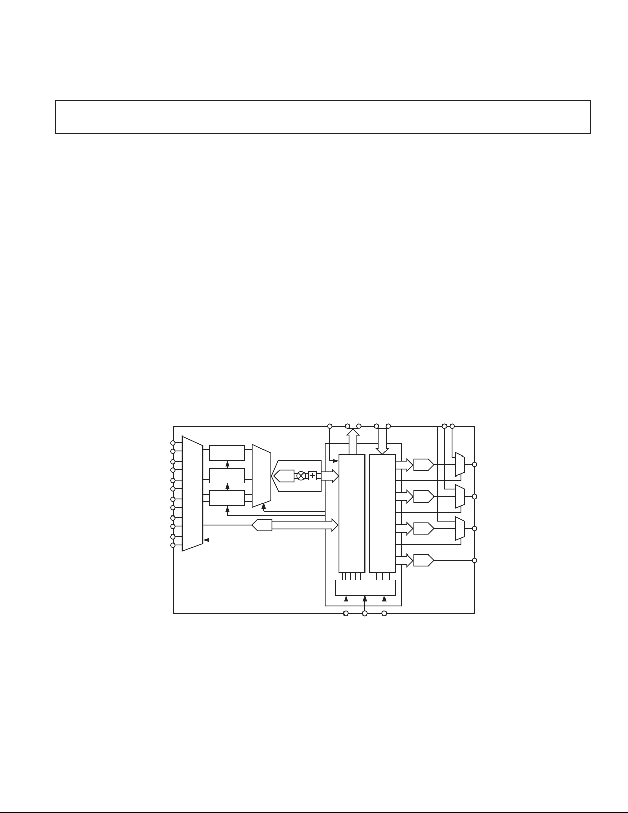
GENERAL DESCRIPTION
The ADV7202 is a video rate sampling Codec.
It has the capability of sampling up to five NTSC/PAL/SECAM
video I/P signals. The resolution on the front-end digitizer is
12 bits; 2 bits (12 dB) are used for gain and offset adjustment.
The digitizer has a conversion rate of 54 MHz.
It also has up to eight auxiliary inputs that can be sampled by
an 843 kHz SAR ADC for system monitoring, etc.
The back end consists of four 10-bit DACs that run at up to
54 MHz and can be used to output CVBS, S-Video, Component
YCrCb, and RGB.
This Codec also supports Picture-on-Picture with the 3-channel
I/P mux that also muxes to the DAC O/Ps.
The ADV7202 can operate at 3.3 V or 5 V. Its monolithic CMOS
construction ensures greater functionality with lower power
dissipation.
The ADV7202 is packaged in a small 64-lead LQFP package.
AIN1P
AIN1M
AIN2P
AIN2M
AIN3P
AIN3M
AIN4P
AIN4M
AIN5P
AIN5M
AIN6P
AIN6M
I/P
MUX
SHA AND
CLAMP
SHA AND
CLAMP
SHA AND
CLAMP
8-BIT 843KHz
ADV7202
FUNCTIONAL BLOCK DIAGRAM
DOUT
DAC DATA
[9:0]
12C/SPI
[9:0]
DAC
LOGIC
MUX
A/D
ADC BLOCK
12-BIT
A/D
XTAL
ADC
LOGIC
10-BIT
D/A
10-BIT
D/A
10-BIT
D/A
10-BIT
D/A
OSD I/P "S"
DAC0
DAC1
DAC2
DAC3
REV. PrB
Information furnished by Analog Devices is believed to be accurate and
reliable. However, no responsibility is assumed by Analog Devices for its
use, nor for any infringements of patents or other rights of third parties that
may result from its use. No license is granted by implication or otherwise
under any patent or patent rights of Analog Devices.
One Technology Way, P.O. Box 9106, Norwood, MA 02062-9106, U.S.A.
Tel: 781/329-4700 www.analog.com
Fax: 781/326-8703 © Analog Devices, Inc., 2002
Page 2

PRELIMINARY TECHNICAL DATA
ADV7202–SPECIFICATIONS
5 V SPECIFICATIONS
(AVDD/DVDD = 5 V ⴞ 5%, V
= 1.235 V R
REF
= 1.2 k⍀, all specifications T
SET
MIN
1
to T
unless otherwise noted.)
MAX
Parameter Min Typ Max Unit Test Conditions
STATIC PERFORMANCE
Resolution (Each DAC) 10 Bits
Accuracy (Each DAC) 10
Integral Nonlinearity ± 2 LSB 10-Bit Operation
Differential Nonlinearity ± 2 LSB 10-Bit Operation
VIDEO ADC
Resolution 10 Bits (plus 2-Bits for gain ranging) 2.2 V Ref.
Accuracy 10
Integral Nonlinearity ± 1 LSB 10-Bit
Differential Nonlinearity ± 0.25 LSB 10-Bit
Input Voltage Range
SNR 62 dB 27 MHz Clock, f
2
–V
REFADC
+V
REFADC
See Figure TBD
= 100 kHz
IN
50 dB 54 MHz Clock, fIN = 100 kHz
AUX ADC
Resolution 8 Bits
Differential Nonlinearity ± 1 LSB Guaranteed Monotonic
Integral Nonlinearity ± 2 LSB
SNR 44 dB 27 MHz Clock
Input Voltage Range 0 2 V
REFADC
V
DIGITAL INPUTS
Input High Voltage, V
Input Low Voltage, V
Input Current, I
Input Capacitance, C
INL
IN
IN
INH
2V
0.8 V
± 1 µA
TBD pF
DIGITAL OUTPUTS
Output High Voltage, V
Output Low Voltage, V
OL
OH
2.4 V I
0.4 V I
SOURCE
= 3.2 mA
SINK
= 400 µA
Three-State Leakage Current 10 µA
Output Capacitance 10 pF
Digital Output Access Time, t
Digital Output Hold Time, t
14
15
8 ns See Figure 16
3ns
ANALOG OUTPUTS
Output Current 4.33 mA R
= 1.2 kΩ, RL = 300 Ω
SET
DAC-to-DAC Matching 2 %
Output Compliance, V
Output Impedance, R
Output Capacitance, C
Analog Output Delay
OC
OUT
3
OUT
0 +1.4 V
50 kΩ
30 pF I
7ns
OUT
= 0 mA
DAC Output Skew 0 ns
VOLTAGE REFERENCE
Reference Range, V
Reference Range, V
Reference Range, V
NOTES
1
0°C to 70°C
2
SHA gain = 1, half range for SHA gain = 2, see Table II.
3
Output Delay measured from 50% of the rising edge of the clock to the 50% point of full-scale transition.
Specifications subject to change without notice.
REFDAC
REFADC
REFADC
1.235 V
2.200 V Programmable 1.1 V or 2.2 V
1.100 V
–2–
REV. PrB
Page 3

PRELIMINARY TECHNICAL DATA
ADV7202
5 V SPECIFICATIONS
(AVDD/DVDD = 5 V ⴞ 5%, V
= 1.235 V R
REF
= 1.2 k⍀, all specifications T
SET
MIN
to T
unless otherwise noted.)
MAX
Parameter Min Typ Max Unit Test Conditions
POWER REQUIREMENTS
1
AVDD/DVDD 4.75 5 5.25 V
Normal Power Mode
I
DAC
I
DSC
I
ADC
2
3
4
4mAR
= 1.2 kΩ, RL = 300 Ω
SET
34 mA
21 mA
Sleep Mode
Current 100 µAR
= 1.2 kΩ, RL = 300 Ω
SET
PSU Rejection Ratio
DACs 0.01 0.5 %/% COMP = 0.1 µF
Video ADC 0.01 0.5 %/%
Aux ADC TBD TBD TBD TBD
Power-Up Time TBD TBD Ref. power-up time
MPU PORT—I
2C5
SCLOCK Frequency 0 400 kHz
SCLOCK High Pulsewidth, t
SCLOCK Low Pulsewidth, t
1
2
Hold Time (Start Condition), t
0.6 µs
1.3 µs
0.6 µs After this period the first clock is
3
generated.
Setup Time (Start Condition), t
Data Setup Time, t
5
SDATA, SCLOCK Rise Time, t
SDATA, SCLOCK Fall Time, t
0.6 µs Relevant for Repeated Start Condition
4
100 ns
6
7
300 ns
300 ns
Setup Time (Stop Condition), t80.6 µs
MPU PORT—SPI
5, 6
SCLOCK Frequency 0 10 MHz
SCLOCK High Pulsewidth, t
SCLOCK Low Pulsewidth, t
SI Data Setup Time, t
SI Data Hold Time, t
19
21
22
20
TBD TBD kHz
TBD TBD ns
TBD TBD ns
TBD TBD ns
RESET Low Time 100 ns
NOTES
1
All DACs and ADCs on.
2
I
is the DAC supply current.
DAC
3
I
is the digital core supply current.
DSC
4
I
is the ADC supply current.
ADC
5
TTL input values are 0 V to 3 V, with input rise/fall times
Timing reference points at 50% for inputs and outputs.
6
See SPI timing diagram Figures 10 and 11.
Specifications subject to change without notice.
≤3 ns, as measured between the 10% and 90% points.
REV. PrB
–3–
Page 4

PRELIMINARY TECHNICAL DATA
ADV7202–SPECIFICATIONS
5 V SPECIFICATIONS
(AVDD/DVDD = 4.75 – 5.25, V
= 1.235 V R
REF
= 1.2 k⍀, all specifications T
SET
MIN
Parameter Min Typ Max Unit Condition
1
to T
unless otherwise noted.)
MAX
2
PROGRAMMABLE GAIN
AMPLIFIER
Video ADC Gain –6 +6 dB Setup Conditions
CLAMP CIRCUITRY
3
Clamp Off Leakage Current TBD µA
Clamp Fine Source/Sink Current 3 µA
Clamp Coarse Source/Sink Current 0.5 mA
CLOCK CONTROL
DACCLK0/1
DACCLK1 80 MHz Single Edge Single Clock Mode
DACCLK1
8
Data Setup Time, t
Data Hold Time, t
Pipeline Delay
6, 7
4
27 MHz Dual CLK Dual Edge Mode
27 MHz 4:2:2 Mode
12
13
5
, t
18
2 ns All Input Modes
2ns
Video ADC TBD Clock Cycles
SAR TBD Clock Cycles
RESET CONTROL
RESET Low Time 10 ns
NOTES
1
Temperature range T
2
The max/min specifications are guaranteed over this range. The max/min values are typical over 4.75 V to 5.25 V range.
3
External clamp capacitor = 0.1 µF.
4
TTL input values are 0 V to 3 V, with input rise/fall times ≤3 ns, measured between the 10% and 90% points. Timing reference points at 50% for inputs and outputs.
Analog output load ≤10 pF.
5
Output delay measured from the 50% point of the rising edge of CLOCK to the 50% point of full scale transition.
6
Maximum clock speed determined by setup and hold conditions.
7
Single DAC only.
8
Guaranteed by Characterization.
Specifications subject to change without notice.
MIN
to T
: 0oC to 70oC.
MAX
–4–
REV. PrB
Page 5

PRELIMINARY TECHNICAL DATA
ADV7202
3.3 V SPECIFICATIONS
(AVDD/DVDD = 3.3 V ⴞ 5%, V
= 1.235 V R
REF
= 1.2 k⍀, all specifications T
SET
MIN
1
to T
unless otherwise noted.)
MAX
Parameter Min Typ Max Unit Test Conditions
STATIC PERFORMANCE
Resolution (Each DAC) 10 Bits
Accuracy (Each DAC) 10
Integral Nonlinearity ± 2 LSB 10-Bit Operation
Differential Nonlinearity ± 2 LSB 10-Bit Operation
VIDEO ADC
Resolution 10 10 Bits (Plus 2-Bits for gain ranging) 2.2 V Ref.
Accuracy 10
Integral Nonlinearity ± 1 LSB 10-Bit
Differential Nonlinearity ± 0.25 LSB 10-Bit
Differential Input Voltage Range
SNR 62 dB 27 MHz Clock, f
2
–V
REFADC
+V
REFADC
See Table II
= 100 kHz
IN
50 dB 54 MHz Clock, fIN = 100 kHz
AUX ADC
Resolution Bits
Differential Nonlinearity ± 1 LSB Guaranteed Monotonic
Integral Nonlinearity ± 2 LSB
SNR 44 dB 27 MHz Clock
Input Voltage Range 0 2 V
REFADC
V
DIGITAL INPUTS
Input High Voltage, V
Input Low Voltage, V
Input Current, I
Input Capacitance, C
INL
IN
IN
INH
2V
0.8 V
± 1 µA
10 pF
DIGITAL OUTPUTS
Output High Voltage, V
Output Low Voltage, V
OL
OH
2.4 V I
0.4 V I
SOURCE
= 3.2 mA
SINK
= 400 µA
Three-State Leakage Current 10 µA
Output Capacitance 30 pF
Digital Output Access Time, t
Digital Output Hold Time, t
14
15
8 ns See Figure 16
3ns
ANALOG OUTPUTS
Output Current 4.33 mA R
DAC-to-DAC Matching 2 %
Output Compliance, V
Output Impedance, R
Output Capacitance, C
Analog Output Delay
OUT
3
OC
OUT
0 1.4 V
50 kΩ
30 pF I
7ns
DAC Output Skew 0 ns
VOLTAGE REFERENCE
Reference Range, V
Reference Range, V
NOTES
1
0°C to 70°C.
2
SHA gain = 1, half range for SHA gain = 2, see Table II.
3
Output delay measured from 50% of the rising edge of the clock to the 50% point of full scale transition.
Specifications subject to change without notice.
REFDAC
REFADC
1.235 V
1.100 V
= 1.2 kΩ, RL = 300 Ω
SET
= 0 mA
OUT
REV. PrB
–5–
Page 6

PRELIMINARY TECHNICAL DATA
ADV7202–SPECIFICATIONS
3.3 V SPECIFICATIONS
(AVDD/DVDD = 3.3 V ⴞ 5%, V
= 1.235 V R
REF
= 1.2 k⍀, all specifications T
SET
MIN
to T
MAX
Parameter Min Typ Max Unit Test Conditions
POWER REQUIREMENTS
1
AVDD/DVDD 3.15 3.3 3.45 V
Normal Power Mode
I
DAC
I
DSC
I
ADC
2
3
4
4mAR
= 1.2 kΩ, RL = 300 Ω
SET
34 mA
21 mA
Sleep Mode
Current 100 µAR
= 1.2 kΩ, RL = 300 Ω
SET
PSU Rejection Ratio
DACs 0.01 0.5 %/% COMP = 0.1 µF
Video ADC 0.01 0.5 %/%
Aux ADC TBD TBD TBD TBD
Power-Up Time TBD TBD TBD
MPU PORT—I
2C5
SCLOCK Frequency 0 400 kHz
SCLOCK High Pulsewidth, t
SCLOCK Low Pulsewidth, t
1
2
Hold Time (Start Condition), t
0.6 µs
1.3 µs
0.6 µs After this period the first clock is
3
generated.
Setup Time (Start Condition), t
Data Setup Time, t
5
SDATA, SCLOCK Rise Time, t
SDATA, SCLOCK Fall Time, t
0.6 µs Relevant for Repeated Start Condition
4
100 ns
6
7
300 ns
300 ns
Setup Time (Stop Condition), t80.6 µs
MPU PORT—SPI
5, 6
SCLOCK Frequency TBD TBD kHz
SCLOCK High Pulsewidth, t
SCLOCK Low Pulsewidth, t
SI Data Setup Time, t
SI Data Hold Time, t
19
21
22
20
TBD TBD kHz
TBD TBD ns
TBD TBD ns
TBD TBD ns
RESET Low Time 100 ns
NOTES
1
All DACs and ADCs on.
2
I
is the DAC supply current.
DAC
3
I
is the digital core supply current.
DSC
4
I
is the ADC supply current.
ADC
5
TTL input values are 0 V to 3 V, with input rise/fall times
6
See SPI timing diagram Figures 10 and 11.
Specifications subject to change without notice.
≤ 3 ns, as measured between the 10% and 90% points. Timing reference points at 50% for inputs and outputs.
unless otherwise noted.)
–6–
REV. PrB
Page 7

PRELIMINARY TECHNICAL DATA
ADV7202
3.3 V SPECIFICATIONS
(AVDD/DVDD = 3.3 V ⴞ 5%, V
= 1.235 V R
REF
= 1.2 k⍀, all specifications T
SET
MIN
Parameter Min Typ Max Unit Condition
1
to T
unless otherwise noted.)
MAX
2
PROGRAMMABLE GAIN
AMPLIFIER
Video ADC Gain –6 +6 dB Setup Conditions
CLAMP CIRCUITRY
3
Clamp Off Leakage Current TBD µA
Clamp Fine Source/Sink Current 3 µA
Clamp Coarse Source/Sink Current 0.5 mA
CLOCK CONTROL
4
DACCLK0/1 27 MHz Dual CLK Dual Edge Mode
DACCLK1 54 MHz Single Edge Dual Clock Mode
DACCLK1 27 MHz 4 : 2 : 2 Mode
Clock High Time, t
Clock Low Time, t
Clock High Time, t
Clock Low Time, t
Data Setup Time, t
Data Hold Time, t
Pipeline Delay
(DACCLK0) 18 ns Dual Edge Dual Clock Mode
10
(DACCLK0) 18 ns
11
(DACCLK1) 18 ns
10
(DACCLK1) 18 ns
11
12
13
5
, t
18
2 ns All Input Modes
2ns
Video ADC TBD Clock Cycles
SAR TBD Clock Cycles
RESET CONTROL
RESET Low Time 10 ns
NOTES
1
Temperature range T
2
The max/min specifications are guaranteed over this range. The max/min values are typical over 3.15 V to 3.45 V range.
3
External clamp capacitor = 0.1 µF.
4
TTL input values are 0 V to 3 V, with input rise/fall times ≤3 ns, measured between the 10% and 90% points. Timing reference points at 50% for inputs and outputs.
Analog output load ≤10 pF.
5
Output delay measured from the 50% point of the rising edge of CLOCK to the 50% point of full-scale transition.
Specifications subject to change without notice.
MIN
to T
: 0oC to 70oC.
MAX
REV. PrB
–7–
Page 8
ADV7202
WARNING!
ESD SENSITIVE DEVICE
PRELIMINARY TECHNICAL DATA
ABSOLUTE MAXIMUM RATINGS
1
AVDD to AVSS . . . . . . . . . . . . . . . . . . . . . . . . . . . . . . . . . 7 V
DVDD to DVSS . . . . . . . . . . . . . . . . . . . . . . . . . . . . . . . . 7 V
Ambient Operating Temperature (T
Storage Temperature (T
Junction Temperature (T
) . . . . . . . . . . . . . . –65°C to +150°C
S
) . . . . . . . . . . . . . . . . . . . . . 150°C
J
) . . . . . . . . 0°C to 70°C
A
Lead Temperature (Soldering, 10 secs) . . . . . . . . . . . . 300°C
Vapor Phase Soldering (1 minute) . . . . . . . . . . . . . . . . 220°C
to GND2 . . . . . . . . . . . . . . . . . . . . . . . . . . . . 0 V to V
I
OUT
NOTES
1
Stresses above those listed under Absolute Maximum Ratings may cause perma-
AA
nent damage to the device. This is a stress rating only; functional operation of the
device at these or any other conditions above those listed in the operational
sections of this specification is not implied. Exposure to absolute maximum rating
conditions for extended periods may affect device reliability.
2
Analog output short circuit to any power supply or common can be of an indefinite
duration.
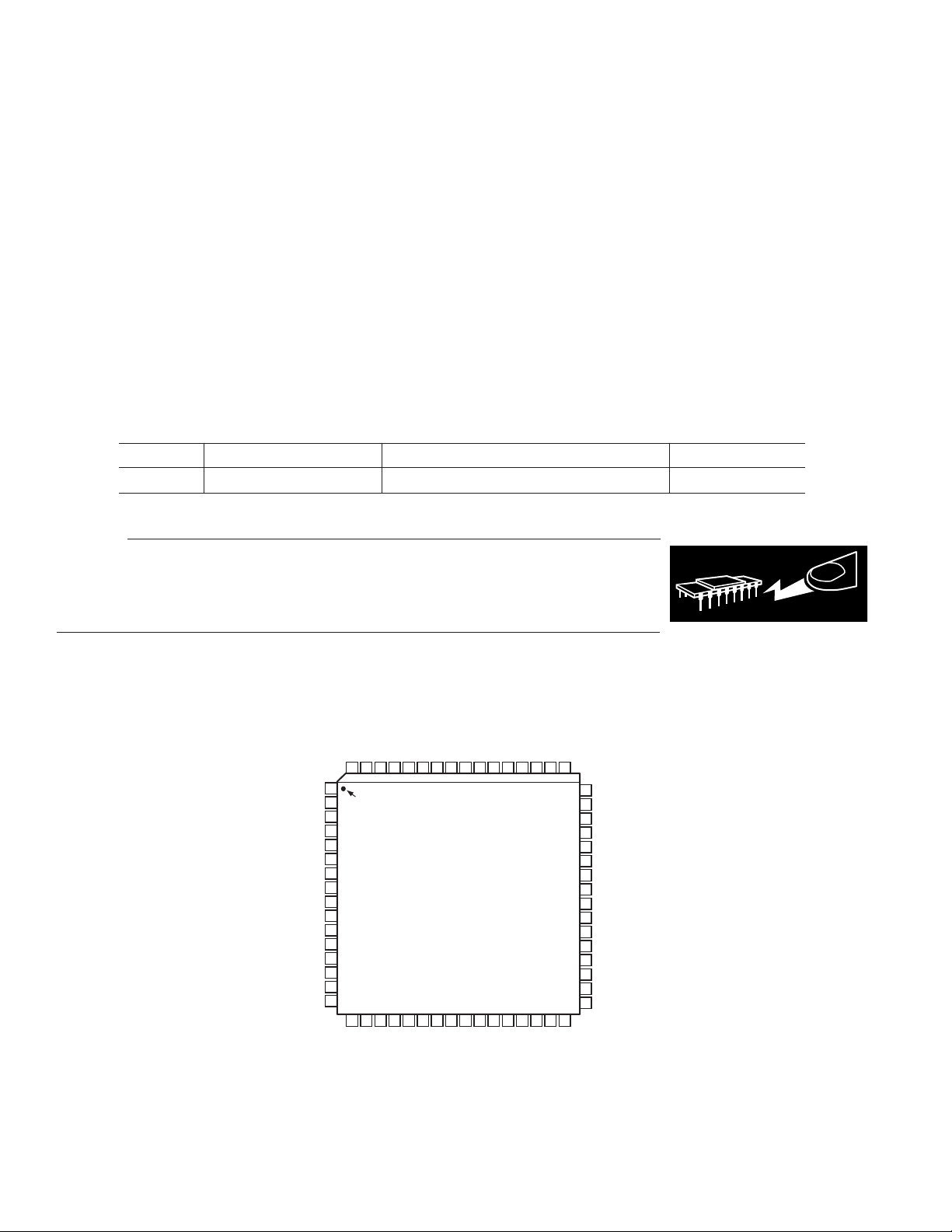
ORDERING INFORMATION
1
Model Temperature Range Package Description Package Option
ADV7202 0°C to 70°C 64-Lead Plastic Quad Flatpack (LQFP) ST-64
CAUTION
ESD (electrostatic discharge) sensitive device. Electrostatic charges as high as 4000 V readily
accumulate on the human body and test equipment and can discharge without detection. Although
the ADV7202 features proprietary ESD protection circuitry, permanent damage may occur on
devices subjected to high-energy electrostatic discharges. Therefore, proper ESD precautions are
recommended to avoid performance degradation or loss of functionality.
SYNC_IN
CLK/SCK
LE/ALSB
XTAL0
XTAL1
AVDD_ADC
AVSS_ADC
AIN1P
AIN1M
AIN2P
AIN12M
AIN3P
AIN3M
AIN4P
AIN4M
AIN5P
PIN CONFIGURATION
SYNC_OUT
DAC_DATA0
DAC_DATA1
DAC_DATA2
DAC_DATA3
DACCLK0
DACCLK1
DAC_DATA4
DAC_DATA5
CAP1
DOUT9
OSDEN
DVDD
DVSS
DOUT8
DOUT7
SI_DATA9
64 63 62 61 60 55 54 53 52 51 50 4959 58 57 56
1
PIN 1
2
IDENTIFIER
3
4
5
6
7
8
9
10
11
12
13
14
15
16
17 18 19 20 21 22 23 24 25 26 27 28 29 30 31 32
AIN6P
AIN5M
AIN6M
SPI_SEL
REFADC
ADV7202
TOP VIEW
(Not to Scale)
CML
CAP2
DAC_DATA6
DAC_DATA7
DAC_DATA8
DAC_DATA9
DOUT6
DOUT5
DOUT3
DOUT4
48
RESET
47
RSET
46
VREFDAC
45
COMP
44
DAC0_OUT
43
DAC1_OUT
42
AVSDD_DAC
41
AVSS_DAC
40
DAC2_OUT
39
DAC3_OUT
38
OSDIN0
37
OSDIN1
36
OSDIN2
35
DOUT0
34
DOUT1
33
DOUT2
–8–
REV. PrB
Page 9

PRELIMINARY TECHNICAL DATA
ADV7202
PIN FUNCTION DESCRIPTIONS
Input/
Pin No. Mnemonic Output Function
1 SYNC_IN I This signal can be used to synchronize the updating of clamps. Polarity is pro-
grammable via I
2 CLK/SCK I MPU Port Serial Interface Clock Input. If the SPI interface is enabled, this pin is
clock input. If the I
3 LE/ALSB I If the SPI interface is enabled, this pin is Latch Enable. If the I
abled, this pin is the ALSB Address Select Pin. This signal sets up the LSB of the
MPU address. MPU address = 2cH, ALSB = 0, MPU address = 2eH, ALSB = 1.
When this pin is tied high, the I
2
I
C interface. When this pin is tied low, the input bandwidth on the I2C lines is
increased.
4 XTAL0 I Input Terminal for crystal oscillator or connection for external oscillator with
CMOS-compatible square wave clock signal.
5 XTAL1 O Second Terminal for Crystal Oscillator. Not connected if external clock source
is used.
6 AVDD_ADC P ADC Analog Supply Voltage (5 V or 3.3 V)
7 AVSS_ADC G Ground for ADC Analog Supply
8–19 AIN1–6 I Analog Signal Inputs. Can be configured differentially or single-ended.
20 SPI_SEL I A high signal on the pin selects SPI MPU port serial operation; a low signal selects
2
I
C MPU port serial operation.
21 REFADC I/O Internally generated Voltage Reference or programmable reference out.
22 CML O Common-Mode Level for ADCs
23, 24 CAP2, CAP1 I ADC Capacitor Network
25 OSDEN I Enable data from OSDIN0–2 to be switched to the outputs when set to a logic high.
26–35 DOUT[9:0] O ADC data output
36 OSDIN2 I Third Input Channel for On-Screen Display
37 OSDIN1 I Second Input Channel for On-Screen Display
38 OSDIN0 I First Input Channel for On-Screen Display
39 DAC3_OUT O General Purpose Analog Output
40 DAC2_OUT O Analog Output. Can Be Used to Output CVBS, R or U
41 AVSS_DAC G Ground for DAC Analog Supply
42 AVDD_DAC P DAC Analog Supply Voltage (5 V or 3.3 V)
43 DAC1_OUT O Analog Output. Can Be Used to Output CVBS, Y, G, or Luma.
44 DAC0_OUT O Analog Output. Can Be Used to Output CVBS, V, B, or Chroma.
45 COMP O Compensation Pin for DACs. Connect 0.1µF capacitor from COMP pin to
AVDD_DAC.
46 VREFDAC I/O DAC Voltage Reference Output Pin, Nominally 1.235 V. Can be driven by an
external voltage reference.
47 RSET I Used to control the amplitude of the DAC output current, 1200 Ω gives an I max
of 4.33 µA.
48 RESET I Master Reset (Asynchronous)
49–52, 55, 56, DAC_DATA[9:0] I DAC Input Data for Four Video Rate DACs
59–62
53 DVSS G Ground for Digital Core Supply
54 DVDD P Analog Supply Voltage for Digital Core (5 V or 3.3 V)
57, 58 DAC_CLK[1:0] I DAC Clocks
63 SYNC_OUT O Output Sync Signal, which goes to a high state while Cr data sample from a
YCrCb data stream or C data from a Y/C data stream is output on DOUT[9:0].
64 SI_SDA I/O If the SPI interface is enabled, this pin is serial data In. If the I
enabled, this pin is MPU Port Serial Data Input/Output.
2
C or SPI.
2
C interface is enabled, this pin is SCK.
2
C filter is activated, which reduces noise on the
2
C interface is en-
2
C interface is
REV. PrB
–9–
Page 10

ADV7202
PRELIMINARY TECHNICAL DATA
FUNCTIONAL DESCRIPTION
Analog Inputs
The ADV7202 has the capability of sampling up to five CVBS
video input signals, or two component YUV, or three S-Video
inputs. Eight auxiliary general-purpose inputs are also available.
Table I shows the analog signal input options available and programmable by I2C/SPI. When configured for auxiliary input
mode, the CVBS inputs are single-ended with the second differential input internally set to VREFADC. The resolution on the
front end digitizer is 12 bits; two bits (12 dB) are used for gain
and offset adjustment. The digitizer has a conversion rate of up
to 54 MHz. The eight auxiliary inputs can be used for system
monitoring, etc., and are sampled by a 843 kHz SAR ADC. The
analog input signal range will be dependent on the value of
VREFADC and the SHA gain see (Table II). Three on-screen
display inputs OSDIN[2:0] mux to the DAC outputs to enable
support for Picture-on-Picture applications.
Table I. Analog Input Signal Data
Register SHA
Setting Description Used Sync_Out
0000 CVBS in on AIN1 0 Figure 1
0001 CVBS in on AIN2 0 Figure 1
0010 CVBS in on AIN3 1 Figure 1
0011 Reserved 1
0100 CVBS in on AIN5 0 Figure 1
0101 CVBS in on AIN6 2 Figure 1
0110 Y/C, Y on AIN1, C on AIN4 0, 1 Figure 2
0111 Y/C, Y on AIN2, C on AIN3 0, 1 Figure 2
1000 YUV, Y on AIN2, U on AIN3, 0, 1, 2 Figure 3
V on AIN6
1001 CVBS on AIN1 and 8 AUX. 0, 1, 2 Figure 1
I/Ps AIN3–6*
1010 CVBS on AIN2 and 8 AUX. 0, 1, 2 Figure 1
I/Ps AIN3–6*
*AUX inputs are single-ended. All other inputs are differential.
Table II. Analog Input Signal Range
I/P SHA Input Range (V)
Mode V
(V) Gain Min Typ Max
REFOUT
Differential 2.2 1 –2.2 0 2.2
Differential 2.2 2 –1.1 0 1.1
Differential 1.1 1 –1.1 0 1.1
Differential 1.1 2 –0.55 0 0.55
Single-ended 2.2 1 0 2.2 4.4
Single-ended 2.2 2 1.1 2.2 3.3
Single-ended 1.1 1 0 1.1 2.2
Single-ended 1.1 2 0.55 1.1 1.65
NOTE
Fclk/32, 843kHz for nominal 27 Mhz
Digital Inputs
The DAC digital inputs on the ADV7202 [9:0] are TTL-compatible. Data may be latched into the device in three different
modes programmable via I
2
C or SPI.
DAC Mode 1, single clock, single edge (see Figure 13) uses only
the rising edge of DAC_CLK1 to latch data into the device.
DAC_CLK0 is a data line that goes high to indicate that the data
is for DAC0. Subsequent data words go to the next DAC in
sequence.
DAC Mode 2, dual edge, dual clock (see Figure 14) clocks data
in on both edges of DAC_CLK0 and DAC_CLK1. Using this
option, data can is latched into the device at four times the
clock speed.
DAC Mode 3, 4:2:2 mode (see Figure 15). Using this option, 4:2:2
video data is latched in using DAC_CLK1, while DAC_CLK0 is used
as a data line that is brought to a high state when Cr data is input;
hence Y will appear on DAC1, Cr on DAC2, and Cb on DAC0.
Analog Outputs
Analog Outputs [DAC0–3] consist of four 10-bit DACs that run at
up to 54 MHz or up to 108 MHz if only DAC0 is used. These outputs
can be used to output CVBS, S-Video, Component YCrCb, and RGB.
Digital Outputs
Video data will be clocked out on DOUT[9:0] during the rising
edge of XTAL0. See Figure 17. Auxiliary data can be read out
2
vial
C compatible MPU port.
I2C and SPI Control
The ADV7202 is both I2C- and SPI-compatible. It should be
noted though that only register write applications are possible
with SPI control. I
2
C operation allows both reading and writing
of system registers. Its operation is explained in detail in the MPU
Port Description section. A logic high level on the SPI_SEL line
selects SPI MPU operation. In this mode the first eight bits of
the 16-bit word on the SI data line will select the register address
and the next eight bits are the value to be programmed into the
register, i.e., the register data. See Figure 10. Latch Enable (LE)
goes low while valid address or data information is present. Figure
10 shows latch enable low for the entire 16 bits of address and
data information. As shown in Figure 11, the register eight-bit data
information does not always have to be clocked in directly after
the address. LE may go high and then low again when valid data
is available. If LE goes low for anything less than eight cycles of
SCLK, the SPI MPU will reset (not register values); hence this
method may be used to initiate a start condition.
–10–
REV. PrB
Page 11

PRELIMINARY TECHNICAL DATA
ADV7202
Video Clamping and AGC Control
When Analog signal clamping is required the input signal should
be AC coupled to the input via a capacitor, the clamping control
is via the MPU port. The AGC is implemented digitally. For
correct operation the user must program the clamp value to which
the signal has been clamped into the ADV7202 I
2
C Register. This
allows the user to specify which signal level is unaffected by the
AGC. The digital output signal will be a function of the ADC
output, the AGC Gain, and the Clamp Level, and can be represented as follows,
D Clamp Level_OUT = ADC Gain ADC – Clamp Level×
[]
()
+
(1)
D_OUT will be a 10-bit number (0–1023), the AGC Gain
defaults to 2 and can have a value between 0 to 7.99. The Clamp
Level is a 10-bit number (0–1023) although only the top eight
bits of clamp level are specified in the I
2
C Register; the ADC
value can be regarded as a 10-bit number (0–1023) for the
equation. It should be noted that the ADC resolution is 12 bits.
The above equation is used to give a basic perspective, and is
mathematically correct.
When the clamps are operational, the operation described by
Equation (1) is how the ADV7202 ensures that the level to
which the user is clamping is unaffected by the AGC loop.
When no clamps are operational, the operation should be
regarded as a straightforward gain-and-level shift.
Equation (1) maps the ADC input voltage range to its output.
AGC Gain
The AGC Gain can be set to a value from 0 to 7.9. The AGC
Gain Register holds a 12-bit number that corresponds to the
required gain. The first three MSBs hold the gain integer value
while the remaining nine bits hold the gain fractional value.
Example: The user requires a gain of 3.65.
The first three bits give the integer value 3, hence these will be
set to ‘0 1 1.’ The remaining nine bits will have to be set to give
the fractional value 0.65, 512 ⫻ 0.65 = 333 = ‘10100110 1.’
From Equation (2) it can be seen that the Clamp Level is
taken from the signal before AGC is applied and then added on
again afterwards; hence, if the AGC Gain is set to a value of
one, the result would be as follows,
(AGC Gain = 1)
D Clamp Level ADC_OUT = ADC - Clamp Level +=
FUNCTIONAL DESCRIPTION
Clamp and AGC Control
(2)
The ADV7202 has a front end 3-channel clamp control. In
order to perform an accurate AGC gain operation, it is necessary to know to what level the user is clamping the black level;
this value is programmable in Clamp Register 0 CR00–CR07.
Each channel has a fine and coarse clamp; the clamp direction
and its duration are programmable. Synchronization of the clamps
and AGC to the input signal is possible using the SYNC_IN control pin and setting mode register CR14 to Logic Level “1.” Using
this method, it is possible to ensure that AGC and clamping are
only applied outside the active video area.
Control Signals
The function and operation of the SYNC_IN signal is described
in the Clamp Control section. The SYNC_OUT will go high
while Cr data from a YCrCb data stream or C data from a Y/C
data stream has been output on DOUT[9:0]. See Figure 1 to
Figure 3.
I2C Filter
A selectable internal I2C filter allows significant noise reduction
on the I
on the I
passed to the I
input bandwidth on the I
2
C interface. In setting ALSB high, the input bandwidth
2
C lines is reduced and pulses of less than 50 ns are not
2
C controller. Setting ALSB low allows greater
2
C lines.
REV. PrB
XTAL0
DAC_DATA [9:0]
SYNC_OUT
XTAL0
DAC_DATA [9:0]
SYNC_OUT
CVBS
Figure 1. SYNC_OUT Output Timing, CVBS Input
YCYC Y CY
Figure 2. SYNC_OUT Output Timing, Y/C (S-VIDEO) Input
CVBS CVBS CVBS CVBS CVBS CVBS
–11–
Page 12

ADV7202
PRELIMINARY TECHNICAL DATA
XTAL0
DAC_DATA [9:0]
SYNC_OUT
CR Y CB Y CR Y CB
Figure 3. SYNC_OUT Output Timing, YCrCb Input
MPU PORT DESCRIPTION
The ADV7202 supports a 2-wire serial (I2C-compatible)
microprocessor bus driving multiple peripherals. Two inputs,
Serial Data (SDA) and Serial Clock (SCL), carry information
between any device connected to the bus. Each slave device is
recognized by a unique address. The ADV7202 has four possible slave addresses for both read and write operations. These
are unique addresses for each device and are illustrated in
Figure 4. The LSB sets either a read or write operation. Logic
Level “1” corresponds to a read operation, while Logic Level
“0” corresponds to a write operation. A1 is set by setting the
ALSB pin of the ADV7202 to Logic Level “0” or Logic Level
“1.” When ALSB is set to “0,” there is greater input bandwidth
on the I
bus. When ALSB is set to “1,” there is reduced input bandwidth on the I
50 ns will not pass into the I
2
C lines, which allows high-speed data transfers on this
2
C lines, which means that pulses of less than
2
C internal controller. This mode is
recommended for noisy systems.
001011A1X
ADDRESS
CONTROL
SET UP BY
ALSB
READ/WRITE
CONTROL
0 DISABLED
1 ENABLED
Figure 4. Slave Address
To control the various devices on the bus, the following protocol must be followed. First the master initiates a data transfer by
establishing a Start condition, defined by a high-to-low transition
on SDA while SCL remains high. This indicates that an address/
data stream will follow. All peripherals respond to the Start
condition and shift the next eight bits (7-bit address + R/W bit).
The bits are tranferred from MSB down to LSB. The peripheral
that recognizes the transmitted address responds by pulling the
data line low during the ninth clock pulse. This is known as an
Acknowledge Bit. All other devices withdraw from the bus at
this point and maintain an idle condition. The idle condition
is where the device monitors the SDA and SCL lines waiting for
the Start condition and the correct transmitted address. The R/W
bit determines the direction of the data.
A Logic “0” on the LSB of the first byte means that the master
will write information to the peripheral. A Logic “1” on the LSB
of the first byte means that the master will read information
from the peripheral.
The ADV7202A acts as a standard slave device on the bus. The
data on the SDA pin is eight bits long, supporting the 7-bit
addresses plus the R/W bit. It interprets the first byte as the
device address and the second byte as the starting subaddress.
The subaddresses auto-increment, allowing data to be written to
or read from the starting subaddress. A data transfer is always
terminated by a Stop condition. The user can access any unique
subaddress register on a one-by-one basis without updating all
the registers.
Stop and Start conditions can be detected at any stage during
the data transfer. If these conditions are asserted out of sequence
with normal read and write operations, they cause an immediate
jump to the idle condition. During a given SCL high period, the
user should only issue one Start condition, one Stop condition,
or a single Stop condition followed by a single Start condition. If
an invalid subaddress is issued by the user, the ADV7202 will
not issue an acknowledge and will return to the idle condition. If
in auto-increment mode, the user exceeds the highest subaddress,
the following action will be taken:
1. In Read Mode, the highest subaddress register contents
will continue to be output until the master device issues a
no-acknowledge. This indicates the end of a read. A
no-acknowledge condition is where the SDA line is not
pulled low on the ninth pulse.
2. In Write Mode, the data for the invalid byte will not be
loaded into any subaddress register, a no-acknowledge will
be issued by the ADV7202, and the part will return to the
idle condition.
Figure 5 illustrates an example of data transfer for a read
sequence and the Start and Stop conditions.
SDATA
SCLOCK
S
START ADDR R /W AC K
1–7 8 9 1–7 8 9 1–7 8 9
SUBADDRESS
ACK DATA
ACK
P
STOP
Figure 5. Bus Data Transfer
–12–
REV. PrB
Page 13

PRELIMINARY TECHNICAL DATA
Figure 6 shows bus write and read sequences.
WRITE
SEQUENCE
SEQUENCE
S SLAVE ADDR A(S) SUB ADDR A(S) DATA A(S ) DATA A(S) P
LSB = 0 LSB = 1
READ
S SLAVE ADDR A(S) SUB ADDR A(S) DATA A( M) DATA A(M) PS SLAVE ADDR A(S)
S = START BIT
P = STOP BIT
A(S) = ACKNOWLEDGE BY SLAVE
A(M) = ACKNOWLEDGE BY MASTER
Figure 6. Write and Read Sequence
t3
SDA
t6
SCL
t2
Figure 7. I2C MPU Port Timing Diagram
t1
t7
ADV7202
A
(S) = NO ACKNOWLEDGE BY SLAVE
A
(M) = NO ACKNOWLEDGE BY MASTER
t
5
t
3
t
4
t
8
DAC_CLK0
DAC_CLK1
DAC_DATA[7:0]
DAC_CLK1
DATA [9:0]
DAC_CLK0
t
12
DATA
t
10
t
13
t
11
DATA
Figure 8. Input Data Format Timing Diagram Single Clock
t
12
DATA
t
13
t
10
t
13
t
12
t
12
t
13
DATADATA
t
11
t
– SETUP TIME
12
–
t
HOLD TIME
13
t
– CLOCK HIGH TIME
10
t
– CLOCK LOW TIME
11
DATA
t
13
t
12
DATA
t
– CLOCK HIGH TIME
10
t
– CLOCK LOW TIME
11
t
– DATA SETUP TIME
12
t
– DATA HOLD TIME
13
REV. PrB
Figure 9. Input Data Format Timing Diagram Dual Clock
–13–
Page 14

ADV7202
PRELIMINARY TECHNICAL DATA
8 CLOCK CYCLES8 CLOCK CYCLES
SCLK
LE
SCLK
LE
SI
ADDRESS [7:0] DATA [7:0]
Figure 10. SPI Timing Mode 1
8 CLOCK CYCLES8 CLOCK CYCLES
SI
NOTE: TAKING LE LOW FOR < 8 CYCLES OF SCLK WILL
RESET THE SPI MPU INTERFACE.
ADDRESS [7:0]
DATA [7:0]
Figure 11. SPI Timing Mode 2
t
SCLK
t
20
19
t
21
SI/LE
Figure 12. SPI Timing Diagram
t
22
–14–
REV. PrB
Page 15

PRELIMINARY TECHNICAL DATA
DIGITAL DATA INPUT TIMING DIAGRAMS
ADV7202
A2 A3
DAC2 DAC0
At A3, NEW DAC0 DATA
IS CLOCKED IN AND A0,
A1, AND A3 ARE SENT TO
THE DACs. DATA APPEARS
AT THE OUTPUT DACs TWO
CLOCK CYCLES AFTER
BEING SENT TO THE DACs.
DAC_CLK1
DAC_CLK0
DAC_DATA [9:0]
A0
DAC0 DAC1 DAC2 DAC0 DAC1
A1
Figure 13. DAC Mode 1, Single Clock, Single Edge Input Data Format Timing Diagram. As with Mode 1, DAC_CLK0 is a
Data Line that Indicates the Data is for DAC0. Above Example Shows Three DAC Usage.
A1 A2 A3 A4
DAC_CLK0
DAC_CLK1
DAC_DATA [9:0]
DAC1 DAC2 DAC3 DAC0
DAC1 DAC2 DAC3 DAC 0
A1 DAC1 DATA CLOCKED IN.
A2 DAC2 DATA CLOCKED IN.
A3 DAC3 DATA CLOCKED IN.
A4 DAC0 DATA FOR THE NEXT
PIXEL AND THE PREVIOUS
FOUR CLOCKED OUT TO DACs.
NOTE
DATA WILL BE CLOCKED TO THE
DACs TWO CLOCK CYCLES
AFTER A4.
Figure 14. DAC Mode 2, Dual Clock, Dual Edge Input Data Format Timing Diagram
DAC_CLK1
DAC_CLK0
DAC_DATA [9:0]
ADC O/P DOUT[9:0]
SYNC_OUT, SYNC_IN
A1 A2 A3 A4
DAC0 DAC1 DAC2 DAC1 DAC0
DAC1 DAC2
Figure 15. DAC Mode 3, 4:2:2 Input Data Format Timing Diagram
t
15
DATADATA
XTAL0
OUTPUT
t
14
t
15
Figure 16. Digital O/P Timing
AT A4, PREVIOUS A0, A2,
AND A3 DATA ARE SENT
TO THE DACs. AT A2, A1
DATA APPEARS AT THE
OUTPUT DACs TWO
CLOCK CYCLES AFTER
BEING SENT T O THE DACs.
t
– ACCESS TIME
14
t
– HOLD TIME
15
REV. PrB
–15–
Page 16

ADV7202
PRELIMINARY TECHNICAL DATA
XTAL0
DATA [9:0]
DATA
DATA DATA DATA DATA DATA DATA DATA
Figure 17. Standard Mode Digital Data O/P Format
REGISTER ACCESSES
The MPU can write to or read from all of the registers of the
ADV7202 except the Subaddress Registers which are writeonly. The Subaddress Register determines which register the
next read or write operation accesses. All communications with
the part through the bus start with an access to the Subaddress
Register. A read/write operation is then performed from/to the
target address which then increments to the next address until a
Stop command on the bus is performed.
REGISTER PROGRAMMING
The following section describes the functionality of each register. All registers can be read from as well as written to.
SR4
ADV7202 SUBADDRESS REGISTER
ADDRESS SR6 SR5 SR4 SR3 SR2 SR1 SR0
00h 0000000 MODE REGISTER 0
01h 0000001 MODE REGISTER 1
02h 0000010 MODE REGISTER 2
03h 0000011 MODE REGISTER 3
04h 0000100 ACG REGISTER 0
05h 0000101 AGC REGISTER 1
06h 0000110 CLAMP REGISTER 0
07h 0000111 CLAMP REGISTER 1
08h 0001000 CLAMP REGISTER 2
09h 0001001 CLAMP REGISTER 3
0Ah 0001010 TIMING REGISTER
0Bh 0001011 V
0Ch 0001100 RESERVED
0Dh 0001101 RESERVED
0Eh 0001110 RESERVED
0Fh 0001111 RESERVED
10h 0010000 AUX REGISTER 0
11h 0010001 AUX REGISTER 1
12h 0010011 AUX REGISTER 2
13h 0010000 AUX REGISTER 3
14h 0010100 AUX REGISTER 4
15h 0010101 AUX REGISTER 5
16h 0010110 AUX REGISTER 6
17h 0010111 AUX REGISTER 7
Subaddress Register (SR7–SR0)
The Communications Register is an 8-bit write-only register.
After the part has been accessed over the bus, and a read/write
operation is selected, the subaddress is set up. The Subaddress
Register determines to/from which register the operation
takes place.
Figure 19 shows the various operations under the control of the
Subaddress Register. “0” should always be written to SR7.
Register Select (SR6–SR0)
These bits are set up to point to the required starting address.
SR3
SR2
ADJUST REGISTER
REF
SR1
SR0SR7 SR6 SR5
Figure 19. Subaddress Registers
–16–
REV. PrB
Page 17

PRELIMINARY TECHNICAL DATA
ADV7202
MODE REGISTER 0
MR0 (MR07–MR00)
(Address (SR4–SR0) = 00H)
Figure 20 shows the various operations under the control of
Mode Register 0.
MR0 BIT DESCRIPTION
ADC Reference Voltage (MR00)
This control bit is used to select the ADC reference voltage.
When this bit is set to “0,” a reference voltage of 1.1 V is
selected. When the bit is set to “1,” a reference voltage of 2.2 V
is selected.
MR7
MR7–MR5
ZERO MUST BE
WRITTEN TO
THESE BITS
MR5
POWER-DOWN
MR14
0 NORMAL
1 POWER-DOWN
MR3
0 NORMAL
1 POWER-DOWN
POWER-DOWN
External Reference Enable (MR01)
Setting this bit to “1” enables an external voltage reference for
the ADC.
Voltage Reference Power-Down (MR02)
Setting this bit to “1” causes the internal ADC voltage reference to
power down.
ADC Power-Down (MR03)
Setting this bit to “1” causes the video rate ADC to power down.
Power-Down (MR04)
Setting this bit to “1” puts the device into power-save mode.
Reserved (MR05–07)
“0” must be written to these bits.
MR2MR4MR6 MR3 MR0
POWER-DOWN
MR2
0 NORMAL
1 POWER-DOWN
ADC
V
MR1
REF
MR1
0 INTERNAL
1 EXTERNAL
EXT REF
ENABLE
ADC REF
VO LTAG E
MR0
0 1.1V
1 2.2V
Figure 20. Mode Register 0
MODE REGISTER 1
MR1 (MR17–MR10)
(Address (SR4–SR0) = 01H)
Figure 21 shows the various operations under the control of
Mode Register 1.
MR1 BIT DESCRIPTION
DAC0 Control (MR10)
Setting this bit to “0” enables DAC 0; otherwise, this DAC is
powered down.
DAC1 Control (MR11)
Setting this bit to “0” enables DAC 1; otherwise, this DAC is
powered down.
DAC2 Control (MR12)
Setting this bit to “0” enables DAC 2; otherwise, this DAC is
powered down.
DAC3 Control (MR13)
Setting this bit to “0” enables DAC 3; otherwise, this DAC is
powered down.
MR17
DAC I/P INVERT
MR17
0 DISABLE
1 ENABLE
4:2:2 MODE
MR16
0 DISABLE
1 ENABLE
MR15
DUAL EDGE CLOCK
MR14
0 SINGLE EDGE
1 DUAL EDGE
DUAL CLOCK
MR15
0 SINGLE CLK
1 DUAL CLK
Dual Edge Clock (MR14)
Setting this bit to “1” allows data to be read into the DACs on
both edges of the clock; hence, data may be read in at twice the
clock frequency. See Figure 21. If this bit is set to “0,” the data
will only be strobed on the rising edge of the clock.
Dual Clock (MR15)
Setting this bit to “1” allows the use of two clocks to strobe data
into the DACs. It is possible to clock data in with only one clock
and use the second clock to contain timing information.
4:2:2 Mode (MR16)
Setting this bit to “1” enables data to be input in 4:2:2 format
(see Figure 21). 4:2:2 mode will only work if TR14 and TR15
register bits are set to zero.
DAC Input Invert (MR17)
Setting this bit to “1” causes the input data to the DACs to be
inverted allowing for an external inverting amplifier.
MR13
MR13
0 NORMAL
1 POWER-DOWN
MR12MR14MR16
DAC2 CONTROL
MR12
0 NORMAL
1 POWER-DOWN
DAC3 CONTROL
MR11
MR10
DAC0 CONTROL
MR10
0 NORMAL
1 POWER-DOWN
DAC1 CONTROL
MR11
0 NORMAL
1 POWER-DOWN
REV. PrB
Figure 21. Mode Register 1
–17–
Page 18

ADV7202
PRELIMINARY TECHNICAL DATA
MODE REGISTER 2
MR2 (MR20–MR27)
(Address (SR4–SR0) = 02H)
Figure 22 shows the various operations under the control of
Mode Register 2.
MR1 BIT DESCRIPTION
Analog Input Configuration (MR20–MR23)
This control selects the analog input configuration, up to six
CVBS input channels, or two component YUV, or three S-Video
and eight auxiliary inputs. See Figure 22 for details.
SHA0 Control (MR24)
Setting this bit to “0” enables SHA0; otherwise, this SHA is
powered down (SHA = Sample and Hold Amplifier).
MR27
AUX CONTROL
MR27
0 NORMAL
1 POWER-DOWN
SHA2 CONTROL
MR26
0 NORMAL
1 POWER-DOWN
SHA0 CONTROL
MR24
0 NORMAL
1 POWER-DOWN
SHA1 CONTROL
MR25
0 NORMAL
1 POWER-DOWN
0 0 0 0 CVBS IN ON AIN1
0 0 0 1 CVBS IN ON AIN2
0 0 1 0 CVBS IN ON AIN3
0 0 1 1 RESERVED
0 1 0 1 CVBS IN ON AIN6
0 1 1 1 Y/C IN ON AIN2, AIN3
1 0 0 0 YUV IN ON AIN2, AIN3, AIN6
1 0 0 1 CVBS IN ON AIN1, 8 AUX INPUTS
SHA1 Control (MR25)
Setting this bit to “0” enables SHA1; otherwise, this SHA is
powered down.
SHA2 Control (MR26)
Setting this bit to “0” enables SHA2; otherwise, this SHA is
powered down.
AUX Control (MR27)
Setting this bit to “0” enables the auxiliary ADC; otherwise, this
Aux ADC is powered down.
MR22MR24MR26 MR23 MR20MR25
MR23 MR22 MR21 MR20
0 1 0 0 CVBS IN ON AIN5
0 1 1 0 Y/C IN ON AIN1, AIN4
1 0 1 0 CVBS IN ON AIN2, 8 AUX INPUTS
*
SEE FIGURE : XX
MR21
ANALOG INPUT CONFIGURATION
*
Figure 22. Mode Register 2
MODE REGISTER 3
MR3 (MR30–MR37)
(Address (SR4–SR0) = 03H)
Figure 23 shows the various operations under the control of
Mode Register 3.
MR3 BIT DESCRIPTION
Clamp Current (MR30)
Setting this bit to “1” enables the doubling of all clamp currents.
Analog Input Mode (MR31)
Setting this bit to “1” enables differential mode for the analog
inputs; otherwise, the inputs are single ended. See Figure 23.
SHA Gain (MR32)
Setting this bit to “0” enables SHA gain of 1. If the bit is set to
“1,” the SHA gain is 2. The SHA gain will limit the input signal
range, see Figure 23.
MR37
MR36–MR37
ZERO MUST BE
WRITTEN TO
THESE REGISTERS
MR35
OUTPUT ENABLE
MR34
0 NORMAL
1 HIGH Z
SYNC POLARITY
MR35
0LOW
1 HIGH
MR33
MR33
0OFF
1ON
Voltage Clamp (MR33)
Setting this bit to “1” will enable the voltage clamps.
Output Enable (MR34)
Setting this bit to “1” puts the digital outputs into high impedance.
SYNC Polarity (MR35)
This bit controls the polarity of the SYNC_IN pin. If the bit
is set to “0,” a logic low pulse corresponds to H-Sync. If the bit
is “1,” a logic high pulse corresponds to H-Sync. This sync in
pulse can then be used to control the synchronization of AGC/
Clamping, see AR12.
Reserved (MR36–MR37)
Zero must be written to both these registers.
MR32MR34MR36
SHA GAIN
MR32
01
12
VOLTAGE CLAMP
MR31
MR30
CLAMP CURRENT
MR30
0 NORMAL
1 DOUBLE
ANALOG INPUT
MR31
0 SINGLE-ENDED
1 POWER-DOWN
Figure 23. Mode Register 3
–18–
REV. PrB
Page 19

PRELIMINARY TECHNICAL DATA
ADV7202
AGC REGISTER 0
AR0 (AR00–AR07)
(Address (SR4–SR0) = 04H)
Figure 24 shows the various operations under the control of
AGC Register 0.
AR0 BIT DESCRIPTION
AGC Multiplier (AR00–AR07)
This register holds the last eight bits of the 12-bit AGC
multiplier word.
AR07
AR15
AR15–AR13
ZERO MUST BE
WRITTEN TO
THESE REGISTERS
ACG SYNC ENABLE
AR12
0OFF
1ON
AGC REGISTER 0
AR1 (AR08–AR15)
(Address (SR4–SR0) = 05H)
Figure 24 shows the various operations under the control of
AGC Register 1.
AR1 BIT DESCRIPTION
AGC Multiplier (AR08–AR11)
These registers hold the first four bits of the 12-bit AGC
multiplier word.
AGC Sync Enable (AR12)
Setting this bit to “1” forces the AGC to wait until the next sync
pulse before switching on.
Reserved (AR13–AR15)
Zero must be written to these registers.
AR02AR04AR06 AR05 AR03
AR10AR12AR14 AR13 AR11
AR09
AR08
AR01
ACG MULTIPLIER
AR11–AR00
12-BIT ACG MULTIPLIER,
HOLDS THE LSB, AR11
THE MSB
AR00
Figure 24. AGC Registers 0–1
REV. PrB
–19–
Page 20

ADV7202
PRELIMINARY TECHNICAL DATA
CLAMP REGISTER 0
CR0 (CR00–CR07)
(Address (SR4–SR0) = 06H)
Figure 25 shows the various operations under the control of
Clamp Register 0.
CR0 BIT DESCRIPTION
Clamp Level/4 (CR00–CR07)
In order to perform an accurate AGC gain operation, it is
necessary to know to what level the user is clamping the black
level. This black level is then subtracted from the 10-bit ADC
output before gaining. It is then added on again afterwards. It
should be noted that this register is eight bit and will hold the
value of Clamp Value/4.
CLAMP REGISTER 1
CR1 (CR10–CR17)
(Address (SR4–SR0) = 07H)
Figure 26 shows the various operations under the control of
Clamp Register 1.
CR07
CR05 CR03
CLAMP LEVEL
CR07–CR00
8-BIT [7:0] CLAMP
LEVEL, CR00 HOLDS THE
LSB, CR07 THE MSB
CR1 BIT DESCRIPTION
Fine Clamp On Time (CR10–CR12)
There are three fine clamp circuits on the chip. This I2C/SPI
word controls the number of clock cycles for which the fine
clamps are switched on per video line. The clamp is switched on
after a SYNC pulse is received on the SYNC_IN pin, provided
the relevant enabling bit is set (see CR16).
Coarse Clamp On Time (CR13–CR15)
There are three coarse clamp circuits on the chip. This I2C
word controls the number of clock cycles for which the fine
clamps are switched on per video line. The clamp is switched on
after a SYNC pulse is received on the SYNC_IN pin, provided
the relevant enabling bit is set (see CR16).
Synchronize Clamps (CR16)
Setting this bit to “1” forces the clamps to wait until the next
sync pulse before switching on.
Reserved (CR17)
Zero must be written to this bit.
CR02CR04CR06
CR01
CR00
CR17
CR17
ZERO MUST BE
WRITTEN TO
THIS BIT
SYNCHRONIZE
CR16
0OFF
1ON
CLAMPS
Figure 25. Clamp Register 0
CR12CR14CR15 CR13 CR10CR16
COARSE CLAMP ON TIME
CR15 CR14 CR13
0 0 0 2 CLOCK CYCLES
0 0 1 4 CLOCK CYCLES
0 1 0 8 CLOCK CYCLES
0 1 1 16 CLOCK CYCLES
1 0 0 32 CLOCK CYCLES
1 0 1 64 CLOCK CYCLES
1 1 0 128 CLOCK CYCLES
1 1 1 256 CLOCK CYCLES
Figure 26. Clamp Register 1
CR11
CR12 CR11 CR10
0 0 0 2 CLOCK CYCLES
0 0 1 4 CLOCK CYCLES
0 1 0 8 CLOCK CYCLES
0 1 1 16 CLOCK CYCLES
1 0 0 32 CLOCK CYCLES
1 0 1 64 CLOCK CYCLES
1 1 0 128 CLOCK CYCLES
1 1 1 256 CLOCK CYCLES
FINE CLAMP ON TIME
–20–
REV. PrB
Page 21

PRELIMINARY TECHNICAL DATA
ADV7202
CLAMP REGISTER 2
CR2 (CR20–CR27)
(Address (SR4–SR0) = 08H)
Figure 27 shows the various operations under the control of
Clamp Register 2.
CR2 BIT DESCRIPTION
Fine Clamp 0 Up/Down (CR20)
This bit controls the direction of fine clamp number 1, valid
only if the clamp is enabled.
Fine Clamp 0 ON/OFF (CR21)
This bit switches fine clamp number 1 on for the prescribed
number of clock cycles (CR10–CR12).
Fine Clamp 1 Up/Down (CR22)
This bit controls the direction of fine clamp number 2, valid
only if the clamp is enabled.
CR27
CR27–CR26
ZERO MUST BE
WRITTEN TO
THESE REGISTERS
FINE CLAMP 2 ON/OFF
CR25
0OFF
1ON
CR25 CR23
FINE CLAMP 2 UP/DOWN
CR24
0DOWN
1UP
FINE CLAMP 1 ON/OFF
CR23
0OFF
1ON
Fine Clamp 1 ON/OFF (CR23)
This bit switches fine clamp number 2 on for the prescribed
number of clock cycles (CR10–CR12).
Fine Clamp 2 Up/Down (CR24)
This bit controls the direction of fine clamp number 3, valid
only if the clamp is enabled.
Fine Clamp 2 ON/OFF (CR25)
This bit switches fine clamp number 3 on for the prescribed
number of clock cycles (CR10–CR12).
Reserved (CR26–CR27)
Zero must be written to these registers.
CR22CR24CR26
FINE CLAMP 1 UP/DOWN
CR22
0DOWN
1UP
FINE CLAMP 0 ON/OFF
CR21
0OFF
1ON
CR21
CR20
FINE CLAMP 0 UP/DOWN
CR20
0DOWN
1UP
Figure 27. Clamp Register 2
CLAMP REGISTER 3
CR3 (CR30–CR37)
(Address (SR4–SR0) = 09H)
Figure 28 shows the various operations under the control of
Clamp Register 3.
CR3 BIT DESCRIPTION
Coarse Clamp 0 Up/Down (CR30)
This bit controls the direction of coarse clamp number 1, valid
only if the clamp is enabled.
Coarse Clamp 0 ON/OFF (CR31)
This bit switches coarse clamp number 1 on for the prescribed
number of clock cycles (CR13–CR15).
CR37
CR37–CR36
ZERO MUST BE
WRITTEN TO
THESE REGISTERS
CR36 CR35
COARSE CLAMP 2 UP/DOWN
CR34
0DOWN
1UP
COARSE CLAMP 2 ON/OFF
CR35
0OFF
1ON
CR34
COARSE CLAMP 1 ON/OFF
CR33
0OFF
1ON
CR33
Coarse Clamp 1 Up/Down (CR32)
This bit controls the direction of coarse clamp number 2, valid
only if the clamp is enabled.
Coarse Clamp 1 ON/OFF (CR33)
This bit switches coarse clamp number 2 on for the prescribed
number of clock cycles (CR13–CR15).
Coarse Clamp 2 Up/Down (CR34)
This bit controls the direction of coarse clamp number 3, valid
only if the clamp is enabled.
Coarse Clamp 2 ON/OFF (CR35)
This bit switches coarse clamp number 3 on for the prescribed
number of clock cycles (CR13–CR15).
Reserved (CR36–CR37)
Zero must be written to these registers.
CR32
COARSE CLAMP 1 UP/DOWN
CR32
0DOWN
1UP
CR31
COARSE CLAMP 0 ON/OFF
CR31
0OFF
1ON
CR30
COARSE CLAMP 0 UP/DOWN
CR30
0DOWN
1UP
REV. PrB
Figure 28. Clamp Register 3
–21–
Page 22

ADV7202
PRELIMINARY TECHNICAL DATA
TIMING REGISTER
TR (TR00–TR07)
(Address (SR4–SR0) = 0AH)
Figure 29 shows the various operations under the control of the
Timing Register.
TR BIT DESCRIPTION
Crystal Oscillator Circuit (TR00)
If this bit is set to “0,” the internal oscillator circuit will be
disabled. Disabling the oscillator circuit is possible when an
external clock module is used, thus, saving power.
ADC Bias Currents (TR01)
If this bit is set to “1,” all analog bias currents will be doubled.
TR07
TR07
ZERO MUST BE
WRITTEN TO
THIS BIT
TR06 TR05
0 0 0ns
0 1 4ns
1 0 6ns
1 1 8ns
CLOCK DELAY
TR04 TR02
ZERO MUST BE
WRITTEN TO
THIS BIT
DUTY CYCLE
TR01
0 INACTIVE
1 ACTIVE
Duty Cycle Equalizer (TR03)
When this bit is set to “1,” the clock duty cycle equalizer circuit
is active. This will only have an effect on the ADC operation.
The digital core clock will not be affected.
Clock Delay (TR05–TR06)
Using these two bits, it is possible to insert a delay in the clock
signal to the digital core. These bits control the insertion of
the delay.
Reserved (TR02, TR04, TR07)
Zero must be written to the bits in these registers.
TR03 TR00
EQUALIZER
TR02TR04TR05TR06
ZERO MUST BE
WRITTEN TO
THIS BIT
TR01
0 NORMAL
1 DOUBLE
TR01
ADC BIAS
CURRENTS
CRYSTAL
OSC. CKT
TR00
0 DISABLE
1 ENABLE
Figure 29. Timing Register 0
VREF ADJUST REGISTER
VR (VR00–VR07)
(Address (SR4–SR0) = 0AH)
Figure 30 shows the various operations under the control of the
VREF Adjust Register.
VR BIT DESCRIPTION
Reserved (VR00)
This register is reserved and “1” must be written to this bit.
VR07
VR07
ZERO MUST BE
WRITTEN TO
THIS BIT
ADC REFERENCE VOLTAGE ADJUST
VR06 VR05 VR04
0 0 0 DEFAULT NOMINAL
0 0 1 +14mV
0 1 0 +28mV
0 1 1 +42mV
10 0 –14mV
10 1 –28mV
11 0 –42mV
11 1 –56mV
Reserved (VR01–VR03)
Zero must be written to these registers.
Reference Voltage Adjust (VR04–VR06)
By setting the value of this 3-bit word, it is possible to trim the
ADC internal voltage reference VREFADC.
Reserved (VR07)
Zero must be written to this register.
VR03 VR00
VR02VR04VR05VR06
VR03–VR01
ZERO MUST BE
WRITTEN TO
THESE BITS
VR01
VR00
ONE MUST BE
WRITTEN TO
THIS BIT
Figure 30. ADC VREF Register
–22–
REV. PrB
Page 23

PRELIMINARY TECHNICAL DATA
ADV7202
AUXILIARY MONITORING REGISTERS
AU (AU00–AU07)
(Address (SR4–SR0) = 10H)
There are eight Auxiliary Monitoring Registers. These registers
are read-only; when the device is configured for auxiliary
inputs, they will display a value corresponding to the converted
AU07
AUX REGISTER0
AU07–AU00
8-BIT [7:0] VALUE
CORRESPONDING TO
AUX0 INPUT VALUE
Figure 31. AUX Register 0
AU15
AUX REGISTER1
AU15–AU08
8-BIT [7:0] VALUE
CORRESPONDING TO
AUX1 INPUT VALUE
auxiliary input. Auxiliary Register “0” will contain the value of
the converted auxiliary “0” input, auxiliary register “1” the
value of the converted auxiliary “1” input, and so on to auxiliary
register 7.
AU03 AU00
AU11 AU08
AU02AU04AU05AU06
AU10AU12AU13AU14
AU01
AU09
AU23
AU31
Figure 32. AUX Register 1
AU19 AU16
AUX REGISTER2
AU23–AU16
8-BIT [7:0] VALUE
CORRESPONDING TO
AUX2 INPUT VALUE
AU18AU20AU21AU22
Figure 33. AUX Register 2
AU27 AU24
AUX REGISTER3
AU31–AU24
8-BIT [7:0] VALUE
CORRESPONDING TO
AUX3 INPUT VALUE
AU26AU28AU29AU30
Figure 34. AUX Register 3
AU17
AU25
REV. PrB
–23–
Page 24

ADV7202
PRELIMINARY TECHNICAL DATA
AU39
AU47
AU55
AU35 AU32
AUX REGISTER4
AU39–AU32
8-BIT [7:0] VALUE
CORRESPONDING TO
AUX4 INPUT VALUE
AU34AU36AU37AU38
Figure 35. AUX Register 4
AU43 AU40
AUX REGISTER5
AU47–AU40
8-BIT [7:0] VALUE
CORRESPONDING TO
AUX5 INPUT VALUE
AU42AU44AU45AU46
Figure 36. AUX Register 5
AU51 AU48
AU50AU52AU53AU54
AU33
AU41
AU49
AU63
AUX REGISTER6
AU55–AU48
8-BIT [7:0] VALUE
CORRESPONDING TO
AUX6 INPUT VALUE
Figure 37. AUX Register 6
AU59 AU56
AUX REGISTER7
AU63–AU56
8-BIT [7:0] VALUE
CORRESPONDING TO
AUX7 INPUT VALUE
AU58AU60AU61AU62
Figure 38. AUX Register 7
AU57
–24–
REV. PrB
Page 25

PRELIMINARY TECHNICAL DATA
ADV7202
CLAMP CONTROL
The clamp control has 2 modes of operation, if the Synchronize
clamp control bit CR16 (bit-6 address 07h) is set to on the
clamps that are enabled will be switched on for the programmed
time when triggered by the Sync_in control signal, this control
signal is edge detected and its polarity can be set by MR35 (bit-5
address 03h). If the Synchronize clamp control bit is set to zero,
when enabled each clamp will switch on for the programmed time,
the enabled signal is edge detected hence the bit must first be
reset to zero before the next enable signal can be implemented.
DAC TERMINATION AND LAYOUT CONSIDERATIONS
The ADV7202 contains an on-board voltage reference. The
VREF pin is normally terminated to AVDD through a 0.1 µF
capacitor when the internal VREF is used. Alternatively, the
ADV7202 can be used with an external VREF (AD589).
Resistor RSET is connected between the RSET pin and AVSS
and is used to control the amplitude of the DAC output current.
I
= 5.196/Rset Amps
MAX
Therefore, a recommended RSET value of 1200 Ω will enable
an I
of 4.43 mA. V
MAX
value of 300 Ω.
The ADV7202 has four analog outputs—DAC0, DAC1, DAC2,
and DAC3. The DACs must be used with external buffer circuits
in order to provide sufficient current to drive an output device.
Suitable op amps are the AD8009, AD8002, AD8001, or AD8057.
PC BOARD LAYOUT CONSIDERATIONS
The ADV7202 is optimally designed for lowest noise performance,
both radiated and conducted noise. To complement the excellent noise performance of the ADV7202, it is imperative that
great care be given to the PC board layout.
The layout should be optimized for lowest noise on the ADV7202
power and ground lines. This can be achieved by shielding the
digital inputs and providing good decoupling. The lead length
between groups of AVDD, AVSS, DVDD, and DVSS pins
should be kept as short as possible to minimize inductive ringing.
It is recommended that a 4-layer printed circuit board be
used, with power and ground planes separating the layer of the
signal carrying traces of the components and solder side layer.
Placement of components should be considered to separate
noisy circuits such as crystal clocks, high-speed logic circuitry,
and analog circuitry.
There should be a separate analog ground plane (AVSS) and a
separate digital ground plane (DVSS).
= Rload × I
MAX
, Rload should have a
MAX
Power planes should encompass a digital power plane (DVDD)
and an analog power plane (AVDD). The analog power plane
should contain the DACs and all associated circuitry, VREF
circuitry. The digital power plane should contain all logic
circuitry. The analog and digital power planes should be individually
connected to the common power plane at one single point through
a suitable filtering device such as a ferrite bead.
DAC output traces on a PCB should be treated as transmission
lines. It is recommended that the DACs be placed as close as
possible to the output connector, with the analog output traces
being as short as possible (less than three inches). The DAC
termination resistors should be placed as close as possible to
the DAC outputs and should overlay the PCB’s ground plane.
As well as minimizing reflections, short analog output traces will
reduce noise pickup due to neighboring digital circuitry.
Supply Decoupling
Noise on the analog power plane can be further reduced by the
use of decoupling capacitors.
Optimum performance is achieved by the use of 0.1 µF ceramic
capacitors. Each of the group of AVDD or DVDD pins should
be individually decoupled to ground. This should be done by
placing the capacitors as close as possible to the device with the
capacitor leads as short as possible, thus minimizing lead
inductance.
Digital Signal Interconnect
The digital signal lines should be isolated as much as possible
from the analog outputs and other analog circuitry. Digital
signal lines should not overlay the analog power plane.
Due to the high clock rates used, long clock lines to the ADV7202
should be avoided to minimize noise pickup.
Any active pull-up termination resistors for the digital inputs
should be connected to the digital power plane and not the
analog power plane.
Analog Signal Interconnect
The ADV7202 should be located as close as possible to the output
connectors, thus minimizing noise pickup and reflections due to
impedance mismatch.
For optimum performance, the analog outputs should each be
source and load terminated, as shown in Figure TBD. The
termination resistors should be as close as possible to the
ADV7202 to minimize reflections.
Any unused inputs should be tied to the ground.
REV. PrB
–25–
Page 26

ADV7202
PRELIMINARY TECHNICAL DATA
OUTLINE DIMENSIONS
Dimensions shown in inches and (mm).
64-Lead Thin Plastic Quad Flatpack (LQFP)
(ST-64B)
0.063 (1.60)
0.030 (0.75)
0.024 (0.60)
0.018 (0.45)
SEATING
VIEW A
MAX
49
PLANE
64
0.057 (1.45)
0.055 (1.40)
0.053 (1.35)
0.006 (0.15)
0.002 (0.05)
ROTATED 90ⴗ CCW
NOTE: CONTROLLING DIMENSIONS ARE IN MILLIMETERS.
0.472 (12.00)
48
PIN 1
1
0.020 (0.50)
BSC
0.003 (0.08)
VIEW A
BSC SQ
TOP VIEW
(PINS DOWN)
0.011 (0.27)
0.009 (0.22)
0.007 (0.17)
0.008 (0.20)
0.004 (0.09)
MAX
3.5ⴗ
7ⴗ
0ⴗ
33
32
0.394
(10.0)
BSC
SQ
17
16
C02602–0–1/02(PrA)
–26–
PRINTED IN U.S.A.
REV. PrB
 Loading...