

Page 1
CMOS, 170 MHz, Triple, 10-Bit
V
FEATURES
170 MSPS throughput rate
Triple, 10-bit digital-to-analog converters (DACs)
SFDR
−70 dB at f
−53 dB at f
RS-343A-/RS-170-compatible output
Complementary outputs
DAC output current range: 2.0 mA to 26.5 mA
TTL-compatible inputs
Internal reference: 1.235 V
Single-supply 3.3 V operation
48-lead LFCSP package
Low power dissipation: 30 mW minimum at 3 V
Low power standby mode: 6 mW typical at 3 V
Supports defense and aerospace applications
(AQEC standard)
Military temperature range: −55°C to +105°C
Controlled manufacturing baseline
One assembly/test site
One fabrication site
Enhanced product change notification
Qualification data available on request
APPLICATIONS
Digital video systems
High resolution color graphics
Digital radio modulation
Image processing
Instrumentation
Video signal reconstruction
= 50 MHz; f
CLK
= 140 MHz; f
CLK
= 1 MHz
OUT
= 40 MHz
OUT
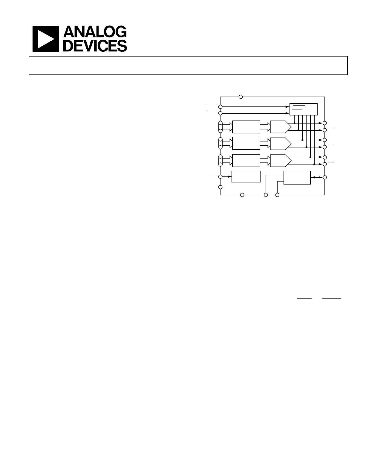
High Speed Video DAC
ADV7123-EP
FUNCTIONAL BLOCK DIAGRAM
AA
BLANK
SYNC
DATA
R9 TO R0
G9 TO G0
B9 TO B0
PSAVE
CLOCK
10
REGISTER
10
REGISTER
10
REGISTER
POWER-DOWN
DATA
DATA
MODE
10
10
10
R
COMPGND
SET
Figure 1.
GENERAL DESCRIPTION
The ADV7123-EP is a triple, high speed digital-to-analog
converter (DAC) on a single monolithic chip. It consists of three
high speed, 10-bit video DACs with complementary outputs,
a standard TTL input interface, and a high impedance, analog
output current source.
The ADV7123-EP has three separate 10-bit-wide input ports.
A single 3.3 V power supply and clock are the only components
required to make the part functional. The ADV7123-EP has
additional video control signals: composite
The ADV7123-EP also has a power save mode.
The ADV7123-EP is fabricated in a 5 V CMOS process. Its
monolithic CMOS construction ensures greater functionality
with lower power dissipation. The ADV7123-EP is available
in a 48-lead LFCSP package.
Full details about this enhanced product are available in the
ADV7123 data sheet, which should be consulted in conjunction
with this data sheet.
PRODUCT HIGHLIGHTS
1. Guaranteed monotonic to 10 bits.
2. Compatible with a wide variety of high resolution color
graphics systems, including RS-343A and RS-170.
DAC
DAC
DAC
REFERENCE
BLANK AND
SYNC LOGIC
VOLTAGE
CIRCUIT
ADV7123-EP
SYNC
and
IOR
IOR
IOG
IOG
IOB
IOB
V
REF
BLANK
09200-001
.
Rev. 0
Information furnished by Analog Devices is believed to be accurate and reliable. However, no
responsibility is assumed by Analog Devices for its use, nor for any infringements of patents or other
rights of third parties that may result from its use. Specifications subject to change without notice. No
license is granted by implication or otherwise under any patent or patent rights of Analog Devices.
Trademarks and registered trademarks are the property of their respective owners.
One Technology Way, P.O. Box 9106, Norwood, MA 02062-9106, U.S.A.
Tel: 781.329.4700 www.analog.com
Fax: 781.461.3113 ©2010 Analog Devices, Inc. All rights reserved.
Page 2

ADV7123-EP
TABLE OF CONTENTS
Features .............................................................................................. 1
Applications ....................................................................................... 1
Functional Block Diagram .............................................................. 1
General Description ......................................................................... 1
Product Highlights ........................................................................... 1
Revision History ............................................................................... 2
Specifications ..................................................................................... 3
Dynamic Specifications ............................................................... 4
REVISION HISTORY
7/10—Revision 0: Initial Version
Timing Specifications ...................................................................5
Absolute Maximum Ratings ............................................................7
ESD Caution...................................................................................7
Pin Configuration and Function Descriptions ..............................8
Outline Dimensions ....................................................................... 10
Ordering Guide .......................................................................... 10
Rev. 0 | Page 2 of 12
Page 3
ADV7123-EP
SPECIFICATIONS
VAA = 3.0 V to 3.6 V, V
Table 1.
Parameter
2
STATIC PERFORMANCE
Resolution (Each DAC) 10 Bits R
Integral Nonlinearity (BSL) −1 +0.5 +1 LSB R
Differential Nonlinearity −1 +0.25 +1 LSB R
DIGITAL AND CONTROL INPUTS
Input High Voltage, VIH 2.0 V
Input Low Voltage, VIL 0.8 V
Input Current, IIN −1 +1 μA VIN = 0.0 V or VDD
PSAVE Pull-Up Current
Input Capacitance, CIN 10 pF
ANALOG OUTPUTS
Output Current 2.0 26.5 mA
DAC-to-DAC Matching 1.0 %
Output Compliance Range, VOC 0 1.4 V
Output Impedance, R
Output Capacitance, C
Offset Error 0 0 % FSR Tested with DAC output = 0 V
Gain Error
3
VOLTAGE REFERENCE, EXTERNAL
Reference Range, V
VOLTAGE REFERENCE, INTERNAL
Voltage Reference, V
POWER DISSIPATION
Digital Supply Current
6.5 12.0 mA f
7.5 13.5 mA f
Analog Supply Current 67 72 mA R
8 mA R
Standby Supply Current 2.1 5.0 mA
Power Supply Rejection Ratio 0.1 0.5 %/%
1
Temperature range T
2
These maximum/minimum specifications are guaranteed by characterization over the 3.0 V to 3.6 V range.
3
Gain error = {(Measured (FSC)/Ideal (FSC) − 1) × 100}, where Ideal (FSC) = V
4
Digital supply is measured with a continuous clock that has data input corresponding to a ramp pattern and with an input level at 0 V and VDD.
= 1.235 V, R
REF
= 560 Ω, CL = 10 pF. All specifications T
SET
MIN
to T
,1 unless otherwise noted; T
MAX
Min Typ Max Unit Test Conditions/Comments
= 680 Ω
SET
= 680 Ω
SET
= 680 Ω
SET
20 μA
Green DAC, SYNC
2.0 18.5 mA
70 kΩ
OUT
10 pF
OUT
RGB DAC, SYNC
0 % FSR FSR = 17.62 mA
1.12 1.235 1.35 V
REF
1.235 V
REF
4
to T
MIN
: −55°C to +105°C.
MAX
2.2 5.0 mA f
× K × (0x3FFH) and K = 7.9896.
REF/RSET
= 50 MHz
CLK
= 140 MHz
CLK
= 170 MHz
CLK
= 560 Ω
SET
= 4933 Ω
SET
= low, digital and control inputs at VDD
PSAVE
= high
= low
J MAX
1
= 110°C.
Rev. 0 | Page 3 of 12
Page 4

ADV7123-EP
DYNAMIC SPECIFICATIONS
VAA = 3.0 V to 3.6 V, V
= 1.235 V, R
REF
= 680 Ω, CL = 10 pF. All specifications are at TA = 25°C, unless otherwise noted; T
SET
J MAX
= 110°C.
Table 2.
Parameter
1
Min Typ Max Unit
AC LINEARITY
Spurious-Free Dynamic Range to Nyquist
2
Single-Ended Output
f
= 50 MHz; f
CLK
f
= 50 MHz; f
CLK
f
= 50 MHz; f
CLK
f
= 50 MHz; f
CLK
f
= 100 MHz; f
CLK
f
= 100 MHz; f
CLK
f
= 100 MHz; f
CLK
f
= 100 MHz; f
CLK
f
= 140 MHz; f
CLK
f
= 140 MHz; f
CLK
f
= 140 MHz; f
CLK
f
= 140 MHz; f
CLK
= 1.00 MHz 67 dBc
OUT
= 2.51 MHz 67 dBc
OUT
= 5.04 MHz 63 dBc
OUT
= 20.2 MHz 55 dBc
OUT
= 2.51 MHz 62 dBc
OUT
= 5.04 MHz 60 dBc
OUT
= 20.2 MHz 54 dBc
OUT
= 40.4 MHz 48 dBc
OUT
= 2.51 MHz 57 dBc
OUT
= 5.04 MHz 58 dBc
OUT
= 20.2 MHz 52 dBc
OUT
= 40.4 MHz 41 dBc
OUT
Double-Ended Output
f
= 50 MHz; f
CLK
f
= 50 MHz; f
CLK
f
= 50 MHz; f
CLK
f
= 50 MHz; f
CLK
f
= 100 MHz; f
CLK
f
= 100 MHz; f
CLK
f
= 100 MHz; f
CLK
f
= 100 MHz; f
CLK
f
= 140 MHz; f
CLK
f
= 140 MHz; f
CLK
f
= 140 MHz; f
CLK
f
= 140 MHz; f
CLK
= 1.00 MHz 70 dBc
OUT
= 2.51 MHz 70 dBc
OUT
= 5.04 MHz 65 dBc
OUT
= 20.2 MHz 54 dBc
OUT
= 2.51 MHz 67 dBc
OUT
= 5.04 MHz 63 dBc
OUT
= 20.2 MHz 58 dBc
OUT
= 40.4 MHz 52 dBc
OUT
= 2.51 MHz 62 dBc
OUT
= 5.04 MHz 61 dBc
OUT
= 20.2 MHz 55 dBc
OUT
= 40.4 MHz 53 dBc
OUT
Spurious-Free Dynamic Range Within a Window
Single-Ended Output
f
= 50 MHz; f
CLK
f
= 50 MHz; f
CLK
f
= 140 MHz; f
CLK
= 1.00 MHz; 1 MHz Span 77 dBc
OUT
= 5.04 MHz; 2 MHz Span 73 dBc
OUT
= 5.04 MHz; 4 MHz Span 64 dBc
OUT
Double-Ended Output
f
= 50 MHz; f
CLK
f
= 50 MHz; f
CLK
f
= 140 MHz; f
CLK
= 1.00 MHz; 1 MHz Span 74 dBc
OUT
= 5.00 MHz; 2 MHz Span 73 dBc
OUT
= 5.00 MHz; 4 MHz Span 60 dBc
OUT
Total Harmonic Distortion
f
= 50 MHz; f
CLK
= 1.00 MHz
OUT
TA = 25°C 66 dBc
T
to T
MIN
f
= 50 MHz; f
CLK
f
= 100 MHz; f
CLK
f
= 140 MHz; f
CLK
65 dBc
MAX
= 2.00 MHz 64 dBc
OUT
= 2.00 MHz 64 dBc
OUT
= 2.00 MHz 55 dBc
OUT
Rev. 0 | Page 4 of 12
Page 5

ADV7123-EP
Parameter
1
Min Typ Max Unit
DAC PERFORMANCE
Glitch Impulse 10 pV-sec
DAC-to-DAC Crosstalk
Data Feedthrough4,
Clock Feedthrough4,
1
These maximum/minimum specifications are guaranteed by characterization over the 3.0 V to 3.6 V range.
2
The ADV7123-EP exhibits high performance when operating with an internal voltage reference, V
3
DAC-to-DAC crosstalk is measured by holding one DAC high while the other two DACs are making low-to-high and high-to-low transitions.
4
Clock and data feedthrough is a function of the amount of overshoot and undershoot on the digital inputs. Glitch impulse includes clock and data feedthrough.
5
TTL input values are 0 V to 3 V, with input rise/fall times of 3 ns, measured at the 10% and 90% points. Timing reference points are 50% for inputs and outputs.
3
5
5
33 dB
23 dB
22 dB
.
REF
TIMING SPECIFICATIONS
VAA = 3.0 V to 3.6 V, V
Table 3.
Parameter
2, 3
ANALOG OUTPUTS
Analog Output Delay t6 7.5 ns
Analog Output Rise/Fall Time
Analog Output Transition Time
Analog Output Skew
CLOCK CONTROL
CLOCK Frequency
Data and Control Setup t1 0.68 ns
Data and Control Hold t2 2.9 ns
CLOCK Period t3 5.88 ns
CLOCK Pulse Width High
CLOCK Pulse Width Low
Pipeline Delay
6
PSAVE Up Time
1
Temperature range T
2
These maximum/minimum specifications are guaranteed by characterization over the 3.0 V to 3.6 V range.
3
Timing specifications are measured with input levels of 3.0 V (VIH) and 0 V (VIL).
4
Rise time was measured from the 10% to 90% point of zero to full-scale transition, fall time from the 90% to 10% point of a full-scale transition.
5
Measured from the 50% point of full-scale transition to within 2% of the final output value.
6
Guaranteed by characterization.
7
f
maximum specification production tested at 125 MHz.
CLK
= 1.235 V, R
REF
4
6
7
6
t
6
t
t
6
to T
MIN
: −55°C to +105°C.
MAX
= 560 Ω, CL = 10 pF. All specifications T
SET
5
MIN
to T
,1 unless otherwise noted; T
MAX
J MAX
= 110°C.
Symbol Min Typ Max Unit Test Conditions/Comments
t7 1.0 ns
t8 15 ns
t9 1 2 ns
f
170 MHz
CLK
2.6 ns f
4
2.6 ns f
5
1.0 1.0 1.0 Clock cycles
PD
t10 4 10
ns
CLK_MAX
CLK_MAX
= 170 MHz
= 170 MHz
Rev. 0 | Page 5 of 12
Page 6

ADV7123-EP
t
3
t
4
t
5
CLOCK
(R9 TO R0, G9 TO G0, B9TO B0,
(IOR, IOR, IOG, IOG, IOB, IOB)
NOTES
1. OUTPUT DELAY (
OF FULL-SCALE TRANSITION.
2. OUTPUT RISE/FALL TIME (
3. TRANSITION TIME (
FINAL OUTPUT VALUE.
DIGITAL INPUTS
SYNC, BLANK)
ANALOG INPUT S
t
) MEASURED FROM THE 50% POINT OF THE RISING EDGE OF CLOCKTO THE 50% POINT
6
t
) MEASURED FRO M THE 50% POINT OF FULL-SCALE TRANSITION TO WITHIN 2% OF THE
8
t
2
t
1
t
) MEASURED BETWEEN THE 10% AND 90% POINTS OF FULL-SCALE TRANSITION.
7
t
6
t
8
Figure 2. Timing Diagram
t
7
09200-002
Rev. 0 | Page 6 of 12
Page 7

ADV7123-EP
ABSOLUTE MAXIMUM RATINGS
Table 4.
Parameter Rating
VAA to GND 7 V
Voltage on Any Digital Pin GND − 0.5 V to VAA + 0.5 V
Ambient Operating Temperature (TA) −55°C to +105°C
Storage Temperature (TS) −65°C to +150°C
Junction Temperature (TJ) 150°C
Lead Temperature (Soldering, 10 sec) 300°C
Vapor Phase Soldering (1 Minute) 220°C
I
to GND1 0 V to VAA
OUT
1
Analog output short circuit to any power supply or common GND can be of
an indefinite duration.
Stresses above those listed under Absolute Maximum Ratings
may cause permanent damage to the device. This is a stress
rating only; functional operation of the device at these or any
other conditions above those indicated in the operational
section of this specification is not implied. Exposure to absolute
maximum rating conditions for extended periods may affect
device reliability.
ESD CAUTION
Rev. 0 | Page 7 of 12
Page 8

ADV7123-EP
PIN CONFIGURATION AND FUNCTION DESCRIPTIONS
R9R8R7R6R5R4R3R2R1R0PSAVE
4847464544434241403938
G0
1
G1
2
G2
3
G3
4
G4
5
G5
6
G6
7
G7
8
G8
9
G9
10
11
BLANK
12
SYNC
NOTES
1. THE EXPOSED PADDLE O N THE UNDERSIDE O F THE PACKAGE
MUST BE SOLDERED TO THE GROUND PLANE T O INCREASE THE
RELIABILITY OF THE SOLDER JOINTS AND TO MAXIMIZE THE
THERMAL CAPABILITY OF THE PACKAGE.
PIN 1
INDICATOR
ADV7123-EP
TOP VIEW
(Not to S cale)
13141516171819
AA
B0B1B2B3B4B5B6B7B8
V
202122
SET
R
37
36
V
REF
35
COMP
34
IOR
33
IOR
32
IOG
31
IOG
V
30
AA
V
29
AA
28
IOB
27
IOB
26
GND
25
GND
24
23
B9
CLOCK
09200-003
Figure 3. Pin Configuration
Table 5. Pin Function Descriptions
Pin No. Mnemonic Description
1 to 10,
14 to 23,
39 to 48
11
G0 to G9,
B0 to B9,
R0 to R9
Composite Blank Control Input (TTL Compatible). A Logic 0 on this control input drives the analog outputs—
BLANK
Red, Green, and Blue Pixel Data Inputs (TTL Compatible). Pixel data is latched on the rising edge of CLOCK.
R0, G0, and B0 are the least significant data bits. Unused pixel data inputs should be connected to either the
regular printed circuit board (PCB) power or ground plane.
IOR, IOB, and IOG—to the blanking level. The BLANK signal is latched on the rising edge of CLOCK. When
BLANK
is a Logic 0, the R0 to R9, G0 to G9, and B0 to B9 pixel inputs are ignored.
12
SYNC
Composite Sync Control Input (TTL Compatible). A Logic 0 on the SYNC input switches off a 40 IRE current
source. The sync current is internally connected to the IOG analog output. SYNC
does not override any other
control or data input; therefore, it should only be asserted during the blanking interval. SYNC is latched on
the rising edge of CLOCK. If sync information is not required on the green channel, the SYNC
tied to Logic 0.
13, 29, 30 VAA Analog Power Supply (3.3 V ± 10%). All VAA pins on the ADV7123-EP must be connected.
24 CLOCK
Clock Input (TTL Compatible). The rising edge of CLOCK latches the R0 to R9, G0 to G9, B0 to B9, SYNC
pixel and control inputs. Typically, the CLOCK input is the pixel clock rate of the video system. CLOCK
BLANK
should be driven by a dedicated TTL buffer.
25, 26 GND Ground. The GND pins must be connected.
27, 31, 33
, IOG, IOR Differential Red, Green, and Blue Current Outputs (High Impedance Current Sources). These RGB video outputs
IOB
are specified to directly drive RS-343A and RS-170 video levels into a doubly terminated 75 Ω coaxial cable.
If the complementary outputs are not required, these outputs should be tied to ground.
28, 32, 34 IOB, IOG, IOR
Red, Green, and Blue Current Outputs (High Impedance Current Sources). These RGB video outputs are specified
to directly drive RS-343A and RS-170 video levels into a doubly terminated 75 Ω coaxial cable. All three current
outputs should have similar output loads whether or not they are all being used.
35 COMP
36 V
REF
Compensation Pin for the Internal Reference Amplifier. A 0.1 μF ceramic capacitor must be connected
between COMP and V
Voltage Reference Input for DACs or Voltage Reference Output (1.235 V). The V
through a 0.1 μF capacitor. However, the ADV7123-EP can be overdriven by an external 1.23 V reference
to V
AA
.
AA
pin is normally terminated
REF
(AD1580), if required.
input should be
, and
Rev. 0 | Page 8 of 12
Page 9

ADV7123-EP
Pin No. Mnemonic Description
37 R
The relationship between R
38
EP Exposed Pad
SET
PSAVE
A resistor (R
) connected between this pin and GND controls the magnitude of the full-scale video signal.
SET
Note that the IRE relationships are maintained, regardless of the full-scale output current. For nominal video
levels into a doubly terminated 75 Ω load, R
The relationship between R
and the full-scale output current on IOG (assuming I
SET
= 530 Ω.
SET
is connected to IOG) is
SYNC
given by
R
(Ω) = 11,445 × V
SET
IOG (mA) = 11,445 × V
IOR, IOB (mA) = 7989.6 × V
The equation for IOG is the same as that for IOR and IOB when SYNC
(V)/IOG (mA)
REF
and the full-scale output current on IOR, IOG, and IOB is given by
SET
(V)/R
REF
(Ω) (SYNC being asserted)
SET
(V)/R
REF
(Ω)
SET
is not being used, that is, SYNC is tied
permanently low.
Power Save Control Pin. Reduced power consumption is available on the ADV7123-EP when this pin is active.
The exposed paddle on the underside of the package must be soldered to the ground plane to increase the
reliability of the solder joints and to maximize the thermal capability of the package.
Rev. 0 | Page 9 of 12
Page 10

ADV7123-EP
OUTLINE DIMENSIONS
PIN 1
INDICATOR
7.00
BSC SQ
0.50
BSC
0.30
0.23
0.18
37
36
EXPOSED
PAD
48
1
P
N
I
4.25
4.10 SQ
3.95
N
I
1
R
O
T
D
C
I
A
12
13
0.25 MIN
FOR PROPER CONNECTION O F
THE EXPOSE D P AD, REFER TO
THE PIN CONF IGURATION AND
FUNCTION DESCRIPTIO NS
SECTION O F THIS DATA S HE ET.
112408-A
0.80
0.75
0.70
SEATING
PLANE
25
TOP VIEW
COMPLIANT TO JEDEC S T ANDARDS M O-220-W KKD.
0.45
0.40
0.35
0.20 REF
24
0.05 MAX
0.02 NOM
COPLANARITY
0.08
BOTTOM VIE W
Figure 4. 48-Lead Lead Frame Chip Scale Package [LFCSP_WQ]
7 mm × 7 mm Body, Very Very Thin Quad
(CP-48-5)
Dimensions shown in millimeters
ORDERING GUIDE
1
Model
ADV7123SCP170EP-RL −55°C to +105°C 170 MHz 48-Lead LFCSP_WQ CP-48-5
1
Available in 3.3 V version only.
Temperature Range Speed Option Package Description Package Option
Rev. 0 | Page 10 of 12
Page 11

ADV7123-EP
NOTES
Rev. 0 | Page 11 of 12
Page 12

ADV7123-EP
NOTES
©2010 Analog Devices, Inc. All rights reserved. Trademarks and
registered trademarks are the property of their respective owners.
D09200-0-7/10(0)
Rev. 0 | Page 12 of 12
 Loading...