

Page 1
Low Cost
a
FEATURES
Precise Compressed Bit Rate Control
Field Independent Compression
Flexible Video Interface Supports All Common
Formats, Including CCIR-656
General Purpose 8-, 16- or 32-Bit Host Interface With
512 Deep 32-Bit FIFO
PERFORMANCE
Real-Time Compression Or Decompression of CCIR-601
And Square Pixel Video:
720 3 288 @ 50 Fields/Sec — PAL
768 3 288 @ 50 Fields/Sec — PAL
720 3 243 @ 60 Fields/Sec — NTSC
640 3 243 @ 60 Fields/Sec — NTSC
Compression Ratios from Visually Loss-Less To 350:1
Visually Loss-Less Compression At 4:1 on Natural
Images (Typical)
APPLICATIONS
Nonlinear Video Editing
Video Capture Systems
Remote CCTV Surveillance
Digital Camcorders
Broadcast Quality Video Distribution Systems
Video Insertion Equipment
Image And Video Archival Systems
Digital Video Tape
High Quality Video Teleconferencing
Multiformat Video Codec
ADV601
GENERAL DESCRIPTION
The ADV601 is a very low cost, single chip, dedicated function,
all digital CMOS VLSI device capable of supporting visually
loss-less to 350:1 real-time compression and decompression of
CCIR-601 digital video at very high image quality levels. The
chip integrates glueless video and host interfaces with on-chip
SRAM to permit low part count, system level implementations
suitable for a broad range of applications.
The ADV601 is a video encoder/decoder optimized for real-time
compression and decompression of interlaced digital video. All
features of the ADV601 are designed to yield high performance
at a breakthrough systems-level cost. Additionally, the unique
sub-band coding architecture of the ADV601 offers you many
application-specific advantages. A review of the General Theory
of Operation and Applying the ADV601 sections will help you
get the most use out of the ADV601 in any given application.
The ADV601 accepts component digital video through the
Video Interface and outputs a compressed bit stream though the
Host Interface in Encode Mode. While in Decode Mode, the
ADV601 accepts a compressed bit stream through the Host
Interface and outputs component digital video through the
Video Interface. The host accesses all of the ADV601’s control
and status registers using the Host Interface. An optional Digital
Signal Processor (DSP) may be used for calculating quantization Bin Widths (BW) (instead of the host); the ADV601 sends
current field statistics and receives Bin Width results as a packet
I/O over the DSP serial port interface. A generic fixed-point DSP
(for instance the ADSP-2105) is more than adequate for these
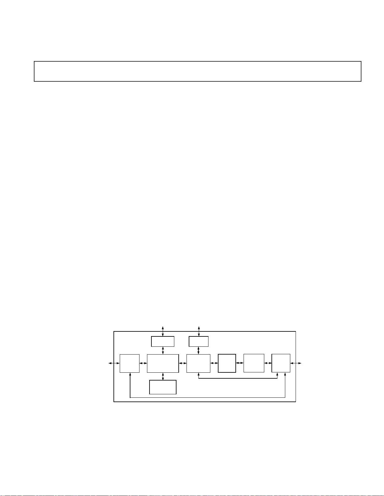
calculations. Figure 1 summarizes the basic function of the part.
FUNCTIONAL BLOCK DIAGRAM
256K X 16-BIT DRAM
(FIELD STORE)
DRAM
MANAGER
DIGITAL
COMPONENT
VIDEO I/O
DIGITAL
VIDEO I/O
PORT
WAVELET
FILTERS,
DECIMATOR, &
INTERPOLATOR
ON-CHIP
TRANSFORM
BUFFER
REV. 0
Information furnished by Analog Devices is believed to be accurate and
reliable. However, no responsibility is assumed by Analog Devices for its
use, nor for any infringements of patents or other rights of third parties
which may result from its use. No license is granted by implication or
otherwise under any patent or patent rights of Analog Devices.
(continued on page 2)
DSP
(OPTIONAL)
SERIAL
PORT
ADAPTIVE
QUANTIZER
One Technology Way, P.O. Box 9106, Norwood, MA 02062-9106, U.S.A.
Tel: 617/329-4700 World Wide Web Site: http://www.analog.com
Fax: 617/326-8703 © Analog Devices, Inc., 1997
RUN
LENGTH
CODER
ADV601
LOW COST, MULTIFORMAT
VIDEO CODEC
HUFFMAN
CODER
HOST
I/O PORT
& FIFO
HOST
Page 2

ADV601
TABLE OF CONTENTS
This data sheet gives an overview of the ADV601 functionality
and provides details on designing the part into a system. The
text of the data sheet is written for an audience with a general
knowledge of designing digital video systems. Where appropriate, additional sources of reference material are noted throughout the data sheet.
GENERAL DESCRIPTION . . . . . . . . . . . . . . . . . . . . . . . . . 1
INTERNAL ARCHITECTURE . . . . . . . . . . . . . . . . . . . . . 3
GENERAL THEORY OF OPERATION . . . . . . . . . . . . . . . 3
References . . . . . . . . . . . . . . . . . . . . . . . . . . . . . . . . . . . . . 3
THE WAVELET KERNEL . . . . . . . . . . . . . . . . . . . . . . . . . 4
THE PROGRAMMABLE QUANTIZER . . . . . . . . . . . . . . . 7
THE RUN LENGTH CODER AND HUFFMAN CODER . . 8
Encoding vs. Decoding . . . . . . . . . . . . . . . . . . . . . . . . . . . 8
PROGRAMMER’S MODEL . . . . . . . . . . . . . . . . . . . . . . . . 8
ADV601 REGISTER DESCRIPTIONS . . . . . . . . . . . . . . . 10
PIN FUNCTION DESCRIPTIONS . . . . . . . . . . . . . . . . . 16
Video Interface . . . . . . . . . . . . . . . . . . . . . . . . . . . . . . . . . 21
Host Interface . . . . . . . . . . . . . . . . . . . . . . . . . . . . . . . . . 25
DSP Interface . . . . . . . . . . . . . . . . . . . . . . . . . . . . . . . . . 25
DRAM Manager . . . . . . . . . . . . . . . . . . . . . . . . . . . . . . . 26
Compressed Data-Stream Definition . . . . . . . . . . . . . . . . 26
APPLYING THE ADV601 . . . . . . . . . . . . . . . . . . . . . . . . . 32
Using the ADV601 in Computer Applications . . . . . . . . 32
Using the ADV601 in Stand-Alone Applications . . . . . . . 32
Connecting the ADV601 to Popular Video Decoders
and Encoders . . . . . . . . . . . . . . . . . . . . . . . . . . . . . . . . 32
GETTING THE MOST OUT OF ADV601 . . . . . . . . . . . 35
ADV601 SPECIFICATIONS . . . . . . . . . . . . . . . . . . . . . . . 36
TEST CONDITIONS . . . . . . . . . . . . . . . . . . . . . . . . . . . . 37
TIMING PARAMETERS . . . . . . . . . . . . . . . . . . . . . . . . . . 37
Clock Signal Timing . . . . . . . . . . . . . . . . . . . . . . . . . . . . 37
CCIR-656 Video Format Timing . . . . . . . . . . . . . . . . . . . 38
Gray Scale/Philips Video Timing . . . . . . . . . . . . . . . . . . . 40
Multiplexed Philips Video Timing . . . . . . . . . . . . . . . . . . 43
Host Interface (Indirect Address, Indirect Register Data,
and Interrupt Mask/Status) Register Timing . . . . . . . . 45
Host Interface (Compressed Data) Register Timing . . . . 47
DSP Interface Timing . . . . . . . . . . . . . . . . . . . . . . . . . . . 49
GENERAL DESCRIPTION
VIDEO INTERFACE
DIGITAL VIDEO IN
(ENCODE)
DIGITAL VIDEO OUT
(DECODE)
(Continued from page 1)
ADV601
LOW COST,
MULTIFORMAT
VIDEO CODEC
HOST INTERFACE
COMPRESSED
VIDEO OUT
(ENCODE)
STATUS & CONTROL
COMPRESSED VIDEO IN
(DECODE)
Figure 1. Functional Block Diagram
The ADV601 adheres to international standard CCIR-601 for
studio quality digital video. The codec also supports a range of
field sizes and rates providing high performance in computer,
PAL, NTSC, or still image environments. The ADV601 is
designed only for real-time interlaced video, full frames of video
are formed and processed as two independent fields of data.
The ADV601 supports the field rates and sizes in Table I. Note
that the maximum active field size is 768 by 288. The maximum
pixel rate is 14.75 MHz.
The ADV601 has a generic 8-/16-/32-bit host interface, which
includes a 512 position, 32-bit wide FIFO for compressed video.
With additional external hardware, the ADV601’s host interface
is suitable (when interfaced to other devices) for moving compressed video over PCI, ISA, SCSI, SONET, 10 Base T, ARCnet,
HDSL, ADSL, and a broad range of digital interfaces. For a full
description of the Host Interface, see the Host Interface section.
The compressed data rate is determined by the input data rate
and the selected compression ratio. The ADV601 can achieve a
near constant compressed bit rate by using the current field
statistics in the off-chip bin width calculator on the external
DSP or Host. The process of calculating bin widths on a DSP
or Host can be “adaptive,” optimizing the compressed bit rate
in real time. This feature provides a near constant bit rate out of
the host interface in spite of scene changes or other types of
source material changes that would otherwise create bit rate
burst conditions. For more information on the quantizer, see
the Programmable Quantizer section.
The ADV601 typically yields visually loss-less compression on
natural images at a 4:1 compression ratio. Desired image quality
levels can vary widely in different applications, so it is advisable
to evaluate image quality of known source material at different
compression ratios to find the best compression range for the
Table I. ADV601 Field Rates and Sizes
Active Active Total Total
Standard Region Region Region Region Field Rate Pixel Rate
Name Horizontal Vertical
1
Horizontal Vertical (Hz) (MHz)
2
CCIR-601/525 720 243 858 262.5 59.94 13.50
CCIR-601/625 720 288 864 312.5 50.00 13.50
Sq. Pixel/525 640 243 780 262.5 59.94 12.27
Sq. Pixel/625 768 288 944 312.5 50.00 14.75
NOTES
1
The maximum active field size is 768 by 288.
2
The maximum pixel rate is 14.75 MHz.
–2–
REV. 0
Page 3
ADV601
application. The sub-band coding architecture of the ADV601
provides a number of options to stretch compression performance. These options are outlined on in the Applying the
ADV601 section.
The DSP serial port interface (SPORT) enables performance of
Bin Width calculations on a DSP instead of the host. The ADV601
transfers current video field statistics to the DSP and receives Bin
Width data from the DSP as packet I/O through the DSP Interface. A generic fixed-point DSP (i.e., the ADSP-2105 low cost,
fixed-point DSP) is more than adequate for these calculations.
INTERNAL ARCHITECTURE
The ADV601 is composed of nine blocks. Four of these blocks
are interface blocks and five are processing blocks. The interface
blocks are the Digital Video I/O Port, the Host I/O Port, external DRAM manager, and the DSP serial I/O Port. The processing blocks are the Wavelet Kernel, the On-Chip Transform
Buffer, the Programmable Quantizer, the Run Length Coder,
and the Huffman Coder.
Digital Video I/O Port
Provides a real-time uncompressed video interface to support a
broad range of component digital video formats, including “D1.”
Host I/O Port and FIFO
Carries control, status, and compressed video to and from the
host processor. A 512 position by 32-bit FIFO buffers the compressed video stream between the host and the Huffman Coder.
DRAM Manager
Performs all tasks related to writing, reading, and refreshing the
external DRAM. The external host buffer DRAM is used for
reordering and buffering quantizer input and output values.
Serial Port (to Optional DSP)
Supports, during encode only, communication of wavelet statistics between the Wavelet Kernel and the DSP and quantizer
control information between the DSP and the Quantizer block.
The user programmed compression ratio is also sent from the
ADV601 host interface to the DSP automatically. Note that a
host processor can be used to replace the DSP functionality in
computer applications.
Wavelet Kernel (Filters, Decimator, and Interpolator)
Gathers statistics on a per field basis and includes a block of
filters, interpolators, and decimators. The kernel calculates
forward and backward bi-orthogonal, two-dimensional, separable wavelet transforms on horizontal scanned video data. This
block uses the internal transform buffer when performing wavelet transforms calculated on an entire image’s data and so
eliminates any need for extremely fast external memories in
an ADV601-based design.
On-Chip Transform Buffer
Provides an internal set of SRAM for use by the wavelet transform kernel. Its function is to provide enough delay line storage
to support calculation of separable two dimensional wavelet
transforms for horizontally scanned images.
Programmable Quantizer
Quantizes wavelet coefficients. Quantize controls are calculated
by the external DSP or host processor during encode operations
and de-quantize controls are extracted from the compressed bit
stream during decode. Each quantizer Bin Width is computed
by the BW calculator software to maintain a constant compressed bit rate or constant quality bit rate. A Bin Width is a per
block parameter the quantizer uses when determining the number of bits to allocate to each block (sub-band).
Run Length Coder
Performs run length coding on zero data and models nonzero
data, encoding or decoding for more efficient Huffman coding.
This data coding is optimized across the sub-bands and varies
depending on the block being coded.
Huffman Coder
Performs Huffman coder and decoder functions on quantized
run-length coded coefficient values. The Huffman coder/decoder uses three ROM-coded Huffman tables that provide excellent performance for wavelet transformed video.
GENERAL THEORY OF OPERATION
The ADV601 processor’s compression algorithm is based on the
bi-orthogonal (7, 9) wavelet transform, and implements field
independent sub-band coding. Sub-band coders transform twodimensional spatial video data into spatial frequency filtered
sub-bands. The quantization and entropy encoding processes
provide the ADV601’s data compression.
The wavelet theory, on which the ADV601 is based, is a new
mathematical apparatus first explicitly introduced by Morlet and
Grossman in their works on geophysics during the mid 80s.
This theory became very popular in theoretical physics and
applied math. The late 80s and 90s have seen a dramatic growth
in wavelet applications such as signal and image processing. For
more on wavelet theory by Morlet and Grossman, see Decompo-
sition of Hardy Functions into Square Integrable Wavelets of Constant Shape (journal citation listed in References section).
ENCODE
PATH
DECODE
PATH
WAVELET
KERNEL
FILTER BANK
ADAPTIVE
QUANTIZER
RUN LENGTH
CODER &
HUFFMAN
CODER
COMPRESSED
DATA
Figure 2. Encode and Decode Paths
References
For more information on the terms, techniques and underlying
principles referred to in this data sheet, you may find the following reference texts useful. A reference text for general digital
video principles is:
Jack, K., Video Demystified: A Handbook for the Digital Engineer
(High Text Publications, 1993) ISBN 1-878707-09-4
Three reference texts for wavelet transform background information are:
Vetterli, M., Kovacevic, J., Wavelets And Sub-band Coding
(Prentice Hall, 1995) ISBN 0-13-097080-8
Benedetto, J., Frazier, M., Wavelets: Mathematics And Applica-
tions (CRC Press, 1994) ISBN 0-8493-8271-8
Grossman, A., Morlet, J., Decomposition of Hardy Functions into
Square Integrable Wavelets of Constant Shape, Siam. J. Math.
Anal., Vol. 15, No. 4, pp 723-736, 1984
REV. 0
–3–
Page 4

ADV601
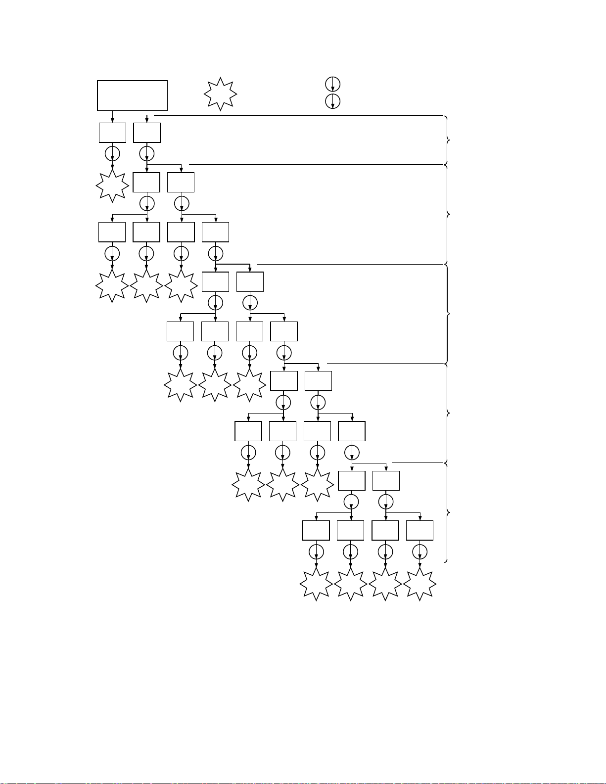
THE WAVELET KERNEL
This block contains a set of filters and decimators that work on
the image in both horizontal and vertical directions. Figure 6
illustrates the filter tree structure. The filters apply carefully
chosen wavelet basis functions that better correlate to the broadband nature of images than the sinusoidal waves used in Discrete Cosine Transform (DCT) compression schemes (JPEG,
MPEG, and H261).
An advantage of wavelet-based compression is that the entire
image can be filtered without being broken into sub-blocks as
required in DCT compression schemes. This full image filtering
eliminates the block artifacts seen in DCT compression and
offers more graceful image degradation at high compression
ratios. The availability of full image sub-band data also makes
image processing, scaling, and a number of other system features possible with little or no computational overhead.
The resultant filtered image is made up of components of the
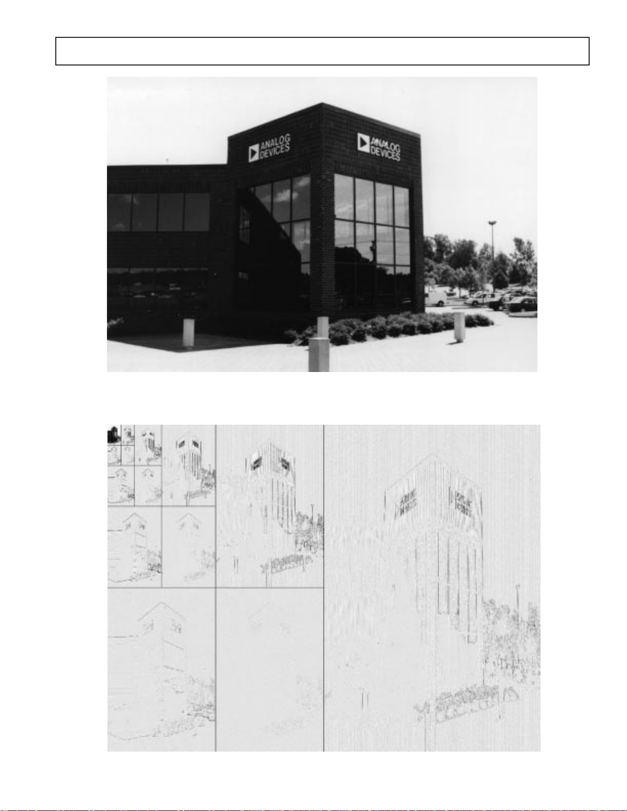
original image as is shown in Figure 3 (a modified Mallat Tree).
Note that Figure 3 shows how a component of video would be
filtered, but in multiple component video luminance and color
components are filtered separately. In Figure 4 and Figure 5 an
actual image and the Mallat Tree (luminance only) equivalent is
shown. It is important to note that while the image has been
filtered or transformed into the frequency domain, no compression has occurred. With the image in its filtered state, it is now
ready for processing in the second block, the quantizer.
Understanding the structure and function of the wavelet filters
and resultant product is the key to obtaining the highest performance from the ADV601. Consider the following points:
• The data in all blocks (except N) for all components are high
pass filtered. Therefore, the mean pixel value in those blocks
is typically zero and a histogram of the pixel values in these
blocks will contain a single “hump” (Laplacian distribution).
• The data in most blocks is more likely to contain zeros or
strings of zeros than unfiltered image data.
• The human visual system is less sensitive to higher frequency
blocks than low ones.
• Attenuation of the selected blocks in luminance or color components results in control over sharpness, brightness, contrast
and saturation.
• High quality filtered/decimated images can be extracted/created
without computational overhead.
Through leverage of these key points, the ADV601 not only
compresses video, but offers a host of application features. Please
see the Applying the ADV601 section for details on getting the
most out of the ADV601’s sub-band coding architecture in
different applications.
NML
BLOCK A IS HIGH PASS IN X AND DECIMATED BY TWO.
BLOCK B IS HIGH PASS IN X, HIGH PASS IN Y, AND DECIMATED BY EIGHT.
BLOCK C IS HIGH PASS IN X, LOW PASS IN Y, AND DECIMATED BY EIGHT.
BLOCK D IS LOW PASS IN X, HIGH PASS IN Y, AND DECIMATED BY EIGHT.
BLOCK E IS HIGH PASS IN X, HIGH PASS IN Y, AND DECIMATED BY 32.
BLOCK F IS HIGH PASS IN X, LOW PASS IN Y, AND DECIMATED BY 32.
BLOCK G IS LOW PASS IN X, HIGH PASS IN Y, AND DECIMATED BY 32.
I
K
H
J
G
F
C
E
A
D
B
BLOCK H IS HIGH PASS IN X, HIGH PASS IN Y, AND DECIMATED BY 128.
BLOCK I IS HIGH PASS IN X, LOW PASS IN Y, AND DECIMATED BY 128.
BLOCK J IS LOW PASS IN X, HIGH PASS IN Y, AND DECIMATED BY 128.
BLOCK K IS HIGH PASS IN X, HIGH PASS IN Y, AND DECIMATED BY 512.
BLOCK L IS HIGH PASS IN X, LOW PASS IN Y, AND DECIMATED BY 512.
BLOCK M IS LOW PASS IN X, HIGH PASS IN Y, AND DECIMATED BY 512.
BLOCK N IS LOW PASS IN X, LOW PASS IN Y, AND DECIMATED BY 512.
Figure 3. Modified Mallat Diagram (Block Letters Correspond to Those in Filter Tree)
–4–
REV. 0
Page 5
ADV601
Figure 4. Unfiltered Original Image (Analog Devices Corporate Offices, Norwood, Massachusetts)
REV. 0
Figure 5. Modified Mallat Diagram of Image
–5–
Page 6
ADV601
LUMINANCE AND
COLOR COMPONENTS
(EACH SEPARATELY)
HIGH
PASS IN
X
X2
BLOCK
A
HIGH
PASS IN
Y
Y
BLOCKBBLOCKCBLOCK
LOW
PASS IN
X
X2
HIGH
PASS IN
LOW
PASS IN
2
Y
LOW
PASS IN
X
Y
2
X
X2X2
HIGH
PASS IN
Y
Y
D
HIGH
PASS IN
Y
Y
INDICATES
CORRESPONDING BLOCK
BLOCK
LETTER ON MALLAT
#
DIAGRAM
X2
INDICATES DECIMATE BY TWO IN X
Y2
INDICATES DECIMATE BY TWO IN Y
STAGE 1
STAGE 2
LOW
PASS IN
Y
2
2
Y
HIGH
PASS IN
X
LOW
PASS IN
X
X2X2
STAGE 3
LOW
PASS IN
2
Y
HIGH
PASS IN
Y
2
Y
LOW
PASS IN
Y
2
Y
2
Y
BLOCKEBLOCKFBLOCK
G
HIGH
PASS IN
Y
2
Y
BLOCKHBLOCKIBLOCK
Figure 6. Wavelet Filter Tree Structure
HIGH
PASS IN
X
LOW
PASS IN
Y
2
Y
LOW
PASS IN
X
X2X2
HIGH
PASS IN
Y
HIGH
PASS IN
Y
Y
BLOCKKBLOCKLBLOCKMBLOCK
LOW
PASS IN
Y
2
J
2
Y
2
Y
HIGH
PASS IN
X
LOW
PASS IN
Y
2
Y
LOW
PASS IN
X
X2X2
HIGH
PASS IN
Y
2
Y
LOW
PASS IN
Y
Y
N
STAGE 4
STAGE 5
2
–6–
REV. 0
Page 7
ADV601
THE PROGRAMMABLE QUANTIZER
This block quantizes the filtered image based on the response
profile of the human visual system. In general, the human eye
cannot resolve high frequencies in images to the same level of
accuracy as lower frequencies. Through intelligent “quantization” of information contained within the filtered image, the
ADV601 achieves compression without compromising the visual
quality of the image. Figure 7 shows the encode and decode
data formats used by the quantizer.
Figure 8 shows how a typical quantization pattern applies over
Mallat block data. The high frequency blocks receive much larger
quantization (appear darker) than the low frequency blocks (appear
lighter). Looking at this figure, one sees some key point concerning
quantization: (1) quantization relates directly to frequency in
Mallat block data and (2) levels of quantization range widely from
high to low frequency block. (Note that the fill is based on a log
formula.) The relation between actual ADV601 bin width factors
and the Mallat block fill pattern in Figure 8 appears in Table II.
Y COMPONENT
393633
24
30
21
27
18
15
6
12
QUANTIZER - ENCODE MODE
9.7
WAVELET
DATA
15.0 BIN
NUMBER
SIGNED SIGNED
UNSIGNED
6.10 1/BW
1/BW
SIGNED
UNSIGNED
8.8 BW
BW
15.17 DATA
0.5
QUANTIZER - DECODE MODE
SIGNED
23.8 DE-QUANTIZED
WAVELET DATA
Figure 7. Programmable Quantizer Data Flow
0
TRNC
SAT
15.0 BIN
NUMBER
9.7
WAVELET
DATA
40
373431
28
41
383532
29
9
3
Cb COMPONENT
25
16
22
13
19
10
7
1
4
Cr COMPONENT
26
17
23
14
20
8
2
REV. 0
11
5
LOW
QUANTIZATION OF MALLAT BLOCKS
HIGH
Figure 8. Typical Quantization of Mallat Data Blocks (Graphed)
–7–
Page 8

ADV601
Table II. ADV601 Typical Quantization of Mallat Data Block
1
Data
Mallat Bin Width Reciprocal Bin
Blocks Factors Width Factors
39 0x007F 0x0810
40 0x009A 0x06a6
41 0x009A 0x06a6
36 0x00BE 0x0564
33 0x00BE 0x0564
30 0x00E4 0x047e
34 0x00E6 0x0474
35 0x00E6 0x0474
37 0x00E6 0x0474
38 0x00E6 0x0474
31 0x0114 0x03b6
32 0x0114 0x03b6
27 0x0281 0x0199
24 0x0281 0x0199
21 0x0301 0x0155
25 0x0306 0x0153
26 0x0306 0x0153
28 0x0306 0x0153
29 0x0306 0x0153
22 0x03A1 0x011a
23 0x03A1 0x011a
5 0x0A16 0x0066
18 0x0A16 0x0066
12 0x0C1A 0x0055
20 0x0C2E 0x0054
19 0x0C2E 0x0054
17 0x0C2E 0x0054
16 0x0C2E 0x0054
14 0x0E9D 0x0046
13 0x0E9D 0x0046
6 0x1DDC 0x0022
9 0x1DDC 0x0022
3 0x23D5 0x001d
11 0x2410 0x001c
10 0x2410 0x001c
8 0x2410 0x001c
7 0x2410 0x001c
5 0x2B46 0x0018
4 0x2B46 0x0018
0 0xA417 0x0006
2 0xC62B 0x0005
1 0xC62B 0x0005
NOTE
1
The Mallat block numbers, Bin Width factors, and Reciprocal Bin Width
factors in Table II correspond to the shading per-cent fill) of Mallat blocks in
Figure 8.
THE RUN LENGTH CODER AND HUFFMAN CODER
This block contains two types of entropy coders that achieve
mathematically loss-less compression: run-length and Huffman.
The run-length coder looks for long strings of zeros and replaces
it with short hand symbols. Table III illustrates an example of
how compression is possible.
The Huffman coder is a digital compressor/decompressor that
can be used for compressing any type of digital data. Essentially,
an ideal Huffman coder creates a table of the most commonly
occurring code sequences (typically zero and small values near
zero) and then replaces those codes with some shorthand. The
ADV601 employs three fixed Huffman tables; it does not create
tables.
The filters and the quantizer increase the number of zeros and
strings of zeros, which improves the performance of the entropy
coders. The higher the selected compression ratio, the more
zeros and small value sequences the quantizer needs to generate.
The transformed image in Figure 5 shows that the filter bank
concentrates zeros and small values in the higher frequency
blocks.
Encoding vs. Decoding
The decoding of compressed video follows the exact path as
encoding but in reverse order. There is no need to calculate Bin
Widths during decode because the Bin Width is stored in the
compressed image during encode.
PROGRAMMER’S MODEL
A host device configures the ADV601 using the Host I/O Port.
The host reads from status registers and writes to control registers through the Host I/O Port.
An optional DSP can perform Bin Width calculations for the
ADV601. The ADV601 can transfer data from component
video statistics registers and receive data for Bin Width registers
as a packet I/O using the DSP I/O Port. Table IV illustrates the
format used to describe the ADV601’s read and write registers.
Table IV. Register Description Conventions
Register Name
Register Type (Indirect or Direct, Read or Write) and Address
Register Functional Description Text
Bit [#] or Bit or Bit Field Name and Usage Description
Bit Range
[High:Low]
0 Action or Indication When Bit Is Cleared (Equals 0)
1 Action or Indication When Bit Is Set (Equals 1)
Table III. Uncompressed Versus Compressed Data Using Run-Length Coding
0000000000000000000000000000000000000000000000000000000000000000000(uncompressed)
57 Zeros (Compressed)
–8–
REV. 0
Page 9
ADV601
REGISTER
ADDRESS
0x0
0x4
0x8
0xC
INDIRECT (INTERNALLY INDEXED) REGISTERS
{ACCESS THESE REGISTERS THROUGH THE
INDIRECT REGISTER ADDRESS AND
INDIRECT REGISTER DATA REGISTERS}
BYTE 3 BYTE 2 BYTE 1
RESERVED
RESERVED
RESERVED
DIRECT (EXTERNALLY ACCESSIBLE) REGISTERS
INDIRECT REGISTER ADDRESS
INDIRECT REGISTER DATA
COMPRESSED DATA
INTERRUPT MASK / STATUS
0x0 0x0983 MODE CONTROL
0x1
0x2
0x3
0x4
0x5
0x6
0x7 – 0x7F
0x80 – 0xA9
0xAA
0xAB
0xAC
0xAD
0xAE
0xAF
0xB0
0xB1
0xB2
0xB3 – 0xFF
0x100
0x101
RESERVED
RESERVED
RESERVED
SUM OF SQUARES [0 – 41]
SUM OF LUMA
SUM OF Cb
SUM OF Cr
MIN LUMA
MAX LUMA
MIN Cb
MAX Cb
MIN Cr
MAX Cr
RESERVED
RBW0
BW0
BYTE 0
FIFO CONTROL
HSTART
HEND
VSTART
VEND
COMPRESS RATIO
RESET
VALUE
0x00
0x00
UNDEF
0x00
0x88
0x000
0x3FF
0x000
0x3FF
UNDEF
UNDEF
UNDEF
UNDEF
UNDEF
UNDEF
UNDEF
UNDEF
UNDEF
UNDEF
UNDEF
UNDEF
UNDEF
UNDEF
UNDEF
REV. 0
0x152
0x153
RBW41
BW41
Figure 9. Map of ADV601 Direct and Indirect Registers
–9–
UNDEF
UNDEF
Page 10

ADV601
ADV601 REGISTER DESCRIPTIONS
Indirect Address Register
Direct (Write) Register Byte Offset 0x00.
This register holds a 16-bit value (index) that selects the indirect register accessible to the host through the indirect data register. All
indirect write registers are 16-bits wide. The address in this register is auto-incremented on each subsequent access of the indirect
data register. This capability enhances I/O performance during modes of operation where the host is calculating Bin Width controls.
In 8-bit mode, auto-increment occurs after writing to Byte 1 (BE1 pin asserted) of the Indirect Data Register; always read or write
Byte 0 then Byte 1 when in 8-bit mode.
[15:0] Indirect Address Register, IAR[15:0]. Holds a 16-bit value (index) that selects the indirect register to read or write through
the indirect data register (undefined at reset)
[31:16] Reserved (undefined read/write zero)
Indirect Register Data
Direct (Read/Write) Register Byte Offset 0x04
This register holds a 16-bit value read or written from or to the indirect register indexed by the Indirect Address Register. In 8-bit
mode, Byte 0 is read or written first followed by Byte 1. This ensures correct operation of auto-increment.
[15:0] Indirect Register Data, IRD[15:0]. A 16-bit value read or written to the indexed indirect register. Undefined at reset.
[31:16] Reserved (undefined read/write zero)
Compressed Data Register
Direct (Read/Write) Register Byte Offset 0x08
This register holds a 32-bit sequence from the compressed video bit stream. This register is buffered by a 512 position, 32-bit FIFO.
Access bytes in the following order for correct auto-increment: Byte 0, Byte 1, Byte 2, then Byte 3. For Word (16-bit) accesses, access Word0 (Byte 0 and Byte 1) then Word1 (Byte 2 and Byte 3). For a description of the data sequence, see the Compressed
Data Stream Definition section.
[31:0] Compressed Data Register, CDR[31:0]. 32-bit value containing compressed video stream data. At reset, contents undefined.
Interrupt Mask / Status Register
Direct (Read/Write) Register Byte Offset 0x0C
This 16-bit register contains interrupt mask and status bits that control the state of the ADV601’s HIRQ pin. With the seven mask
bits (IE_LCODE, IE_STATSR, IE_FIFOSTP, IE_FIFOSRQ, IE_FIFOERR, IE_CCIRER, IE_MERR); select the conditions that
are ORed together to determine the output of the HIRQ pin.
Six of the status bits (LCODE, STATSR, FIFOSTP, MERR, FIFOERR, CCIRER) indicate active interrupt conditions and are
sticky bits that stay set until read. Because sticky status bits are cleared when read, and these bits are set on the positive edge of the
condition coming true, they cannot be read or tested for stable level true conditions multiple times.
The FIFOSRQ bit is not sticky. This bit can be polled to monitor for a FIFOSRQ true condition. Note: Enable this monitoring by
using the FIFOSRQ bit and correctly programming DSL and ESL fields within the FIFO control registers.
[0] CCIR-656 Error in CCIR-656 data stream, CCIRER. This read only status bit indicates the following:
0 No CCIR-656 Error condition, reset value
1 Unrecoverable error in CCIR-656 data stream (missing sync codes)
[1] Statistics Ready, STATSR. This read only status bit indicates the following:
0 No Statistics Ready condition, reset value (STATS_R pin LO)
1 Statistics Ready for BW calculator (STATS_R pin HI)
[2] Last Code Read, LCODE. This read only status bit indicates the last compressed data word for field will be
retrieved from the FIFO on the next read from the host bus.
0 No Last Code condition, reset value (LCODE pin LO)
1 Next read retrieves last word for field in FIFO (LCODE pin HI)
[3] FIFO Service Request, FIFOSRQ. This read only status bit indicates the following:
0 No FIFO Service Request condition, reset value (FIFO_SRQ pin LO)
1 FIFO is nearly full (encode) or nearly empty (decode) (FIFO_SRQ pin HI)
–10–
REV. 0
Page 11

ADV601
[4] FIFO Error, FIFOERR. This condition indicates that the host has been unable to keep up with the ADV601’s compressed
data supply or demand requirements. If this condition occurs during encode, the data stream will not be corrupted until
MERR indicates that the DRAM is also overflowed. If this condition occurs during decode, the video output will be
corrupted. If the system overflows the FIFO (disregarding a FIFOSTP condition) with too many writes in decode mode,
FIFOERR is asserted. This read only status bit indicates the following:
0 No FIFO Error condition, reset value (FIFO_ERR pin LO)
1 FIFO overflow (encode) or underflow (decode) (FIFO_ERR pin HI)
[5] FIFO Stop, FIFOSTP. This condition indicates that the FIFO is full in decode mode and empty in encode mode.
In decode mode only, FIFOSTP status actually behaves more conservatively than this. In decode mode, even when
FIFOSTP is indicated, there are still 32 empty Dwords available in the FIFO and 32 more Dword writes can safely
be performed. This status bit indicates the following:
0 No FIFO Stop condition, reset value (FIFO_STP pin LO)
1 FIFO empty (encode) or full (decode) (FIFO_STP pin HI)
[6] Memory Error, MERR. This condition indicates that an error has occurred at the DRAM memory interface. This condition can
be caused by a defective DRAM, the inability of the Host to keep up with the ADV601 compressed data stream, or bit errors in
the data stream. Note that the ADV601 recovers from this condition without host intervention.
0 No memory error condition, reset value
1 Memory error
[7] Reserved (always read/write zero)
[8] Interrupt Enable on CCIRER, IE_CCIRER. This mask bit selects the following:
0 Disable CCIR-656 data error interrupt, reset value
1 Enable interrupt on error in CCIR-656 data
[9] Interrupt Enable on STATR, IE_STATR. This mask bit selects the following:
0 Disable Statistics Ready interrupt, reset value
1 Enable interrupt on Statistics Ready
[10] Interrupt Enable on LCODE, IE_LCODE. This mask bit selects the following:
0 Disable Last Code Read interrupt, reset value
1 Enable interrupt on Last Code Read from FIFO
[11] Interrupt Enable on FIFOSRQ, IE_FIFOSRQ. This mask bit selects the following:
0 Disable FIFO Service Request interrupt, reset value
1 Enable interrupt on FIFO Service Request
[12] Interrupt Enable on FIFOERR, IE_FIFOERR. This mask bit selects the following:
0 Disable FIFO Stop interrupt, reset value
1 Enable interrupt on FIFO Stop
[13] Interrupt Enable on FIFOSTP, IE_FIFOSTP. This mask bit selects the following:
0 Disable FIFO Error interrupt, reset value
1 Enable interrupt on FIFO Error
[14] Interrupt Enable on MERR, IE_MERR. This mask bit selects the following:
0 Disable memory error interrupt, reset value
1 Enable interrupt on memory error
[15] Reserved (always read/write zero)
Mode Control Register
Indirect (Write Only) Register Index 0x00
This register holds configuration data for the ADV601’s video interface format and controls several other video interface features.
For more information on formats and modes, see the Video Interface section. Bits in this register have the following functions:
[3:0] Video Interface Format, VIF[3:0]. These bits select the interface format. Valid settings include the following (all
other values are reserved):
0x0 CCIR-656
0x2 MLTPX (Philips)
0x3 Philips, reset value
0x8 Gray Scale
[4] VCLK Output Divided by two, VCLK2. This bit controls the following:
0 Do not divide VCLK output (VCLKO = VCLK), reset value
1 Divide VCLK output by two (VCLKO = VCLK/2)
REV. 0
–11–
Page 12

ADV601
[5] Video Interface Master/Slave Mode Select, M/S. This bit selects the following:
0 Slave mode video interface (External control of video timing, HSYNC-VSYNC-FIELD are inputs), reset value
1 Master mode video interface (ADV601 controls video timing, HSYNC-VSYNC are outputs)
[6] Video Interface 525/625 (NTSC/PAL) Mode Select, P/N. This bit selects the following:
0 525 mode video interface, reset value
1 625 mode video interface
[7] Video Interface Encode/Decode Mode Select, E/D. This bit selects the following:
0 Decode mode video interface (compressed-to-raw)
1 Encode mode video interface (raw-to-compressed), reset value
[8] Video Interface Square Pixel Mode Enable, SPE. This bit selects the following:
0 Disable Square Pixel mode video interface
1 Enable Square Pixel mode video interface, reset value
[9] Video Interface Bipolar/Unipolar Color Component Select, BUC. This bit selects the following:
0 Bipolar color component mode video interface, reset value
1 Unipolar color component mode video interface
[10] External DSP Select for bin width calculations, DSP. This bit selects the following:
0 Host provides bin width calculation, reset value
1 External DSP provides bin width calculation
[11] Video Interface Software Reset, SWR. This bit has the following effects on ADV601 operations:
0 Normal operation
1 Software Reset. This bit is set on hardware reset and must be cleared before the ADV601 can begin processing. (reset value)
When this bit is set during encode, the ADV601 completes processing the current field then suspends operation until the
SWR bit is cleared. When this bit is set during decode, the ADV601 suspends operation immediately and does not resume
operation until the SWR bit is cleared. Note that this bit must be set whenever any other bit in the Mode register is changed.
[12] HSYNC pin Polarity, PHSYNC. This bit has the following effects on ADV601 operations:
0 HSYNC is HI during blanking, reset value
1 HSYNC is LO during blanking (HI during active)
[13] HIRQ pin Polarity, PHIRQ. This bit has the following effects on ADV601 operations:
0 HIRQ is active LO, reset value
1 HIRQ is active HI
[15:14] Reserved (always write zero)
FIFO Control Register
Indirect (Read/Write) Register Index 0x01
This register holds the service-request settings for the ADV601’s host interface FIFO, causing interrupts for the “nearly full” and
“nearly empty” levels. Because each register is four bits in size, and the FIFO is 512 positions, the 4-bit value must be multiplied by
32 (decimal) to determine the exact value for encode service level (nearly full) and decode service level (nearly empty). The ADV601
uses these setting to determine when to generate a FIFO Service Request related host interrupt (FIFOSRQ bit and FIFO_SRQ pin).
[3:0] Encode Service Level, ESL[3:0]. The value in this field determines when the FIFO is considered nearly full on encode; a condi-
tion that generates a FIFO service request condition in encode mode. Since this register is four bits (16 states), and the FIFO is
512 positions, the step size for each bit in this register is 32 positions. The following table summarizes sample states of the
register and their meaning.
ESL Interrupt When . . .
0000 Disables service requests (FIFO_SRQ never goes HI during encode)
0001 FIFO has only 32 positions filled (FIFO_SRQ when >= 32 positions are filled)
1000 FIFO is 1/2 full, reset value
1111 FIFO has only 32 positions empty (480 positions filled)
[7:4] Decode Service Level, DSL[7:4]. The value in this field determines when the FIFO is considered nearly empty in decode; a
condition that generates a FIFO service request in decode mode. Because this register is four bits (16 states), and the FIFO
is 512 positions, the step size for each bit in this register is 32 positions. The following table summarizes sample states of the
register and their meaning.
DSL Interrupt When . . .
0000 Disables service requests (FIFO_SRQ never goes HI)
0001 FIFO has only 32 positions filled (480 positions empty)
1000 FIFO is 1/2 empty, reset value
1111 FIFO has only 32 positions empty (FIFO_SRQ when >= 32 positions are empty)
[15:8] Reserved (always write zero)
–12–
REV. 0
Page 13

ADV601
S
VIDEO AREA REGISTERS
The area defined by the HSTART, HEND, VSTART and VEND registers is the active area that the wavelet kernel processes. Video
data outside the active video area is set to minimum luminance and zero chrominance (black) by the ADV601. These registers allow
cropping of the input video during compression (encode only), but do not change the image size. Figure 10 shows how the video area
registers work together.
0, 0
VSTART
H
TART HEND
ZERO
ZERO
ZERO
VEND
ZERO
ZERO
ACTIVE VIDEO AREA
ZERO
MAX FOR SELECTED VIDEO MODE
ZERO
ZERO
X, Y
Figure 10. Video Area and Video Area Registers
HSTART Register
Indirect (Write Only) Register Index 0x02
This register holds the setting for the horizontal start of the ADV601’s active video area. The value in this register is usually set to
zero, but in cases where you wish to crop incoming video it is possible to do so by changing HST.
[9:0] Horizontal Start, HST[9:0]. 10-bit value defining the start of the active video region. (0 at reset)
[15:10] Reserved (always write zero)
HEND Register
Indirect (Write Only) Register Index 0x03
This register holds the setting for the horizontal end of the ADV601’s active video area. If the value is larger than the max size of the
selected video mode, the ADV601 uses the max size of the selected mode for HEND.
[9:0] Horizontal End, HEN[9:0].10-bit value defining the end of the active video region. (0x3FF at reset this value is larger than
the max size of the largest video mode)
[15:10] Reserved (always write zero)
VSTART Register
Indirect (Write Only) Register Index 0x04
This register holds the setting for the vertical start of the ADV601’s active video area. The value in this register is usually set to zero
unless you want to crop the active video.
To vertically crop video while encoding, program the VSTART and VEND registers with actual video line numbers, which differ for
each field. The VSTART and VEND contents must be updated on each field. Perform this updating as part of the field-by-field BW register update process. To perform this dynamic update correctly, the update software must keep track of which field is being processed next.
[9:0] Vertical Start, VST[9:0]. 10-bit value defining the starting line of the active video region, with line numbers from 1-to-625
in PAL and 1-to-525 in NTSC. (0 at reset)
[15:10] Reserved (always write zero)
VEND Register
Indirect (Write Only) Register Index 0x05
This register holds the setting for the vertical end of the ADV601’s active video area. If the value is larger than the max size of the
selected video mode, the ADV601 uses the max size of the selected mode for VEND.
To vertically crop video while encoding, program the VSTART and VEND registers with actual video line numbers, which differ for
each field. The VSTART and VEND contents must be updated on each field. Perform this updating as part of the field-by-field BW
register update process. To perform this dynamic update correctly, the update software must keep track of which field is being processed next.
[9:0] Vertical End, VEN[9:0]. 10-bit value defining the ending line of the active video region, with line numbers from 1-to-625
in PAL and 1-to-525 in NTSC. (0x3FF at reset—this value is larger than the max size of the largest video mode)
[15:10] Reserved (always write zero)
REV. 0
–13–
Page 14

ADV601
Compression Ratio Register
Indirect (Write Only) Register Index 0x06
This register holds the value that is used by the DSP to control compression during encode mode. Note that this register should only
be used when a DSP is calculating Bin Widths.
[7:0] Compression Ratio, CRA[7:0]. Value passed to the DSP during encode operation. The 8-bit value in this field is sent to the
DSP through the serial interface during DSP-assisted encode operations. CRA values are zero-filled from the MSB and one
each is sent to the DSP as part of the packet of data on which the ratio is applied. The DSP software uses the CRA value
and other statistics to calculate BW controls for the ADV601’s quantizer. Note that the relationship between CRA and the
actual compression ratio is dependent on the BW control algorithm used in the DSP (undefined at reset).
[15:8] Reserved (always write zero)
Sum of Squares [0–41] Registers
Indirect (Read Only) Register Index 0x080 through 0x0A9
The Sum of Squares [0–41] registers hold values that correspond to the summation of values (squared) in corresponding Mallat
blocks [0–41]. These registers let the Host or DSP read sum of squares statistics from the ADV601; using these values (with the Sum
of Value, MIN Value, and MAX Value) the host or DSP can then calculate the BW and RBW values. The ADV601 indicates that
the sum of squares statistics have been updated by setting (1) the STATR bit and asserting the STAT_R pin. Read the statistics at
any time. The Host reads these values through the Host Interface or the DSP receives these values through the serial port.
[15:0] Sum of Squares, STS[15:0]. 16-bit values [0-41] for corresponding Mallat blocks [0-41] (undefined at reset). Sum of Square
values are 16-bit codes that represent the Most Significant Bits of values ranging from 40 bits for small blocks to 48 bits for
large blocks. The 16-bit codes have the following precision:
Blocks Precision Sum of Squares Precision Description
0–2 48.–32 48.-bits wide, left shift code by 32-bits, and zero fill
3–11 46.–30 46.-bits wide, left shift code by 30-bits, and zero fill
12–20 44.–28 44.-bits wide, left shift code by 28-bits, and zero fill
21–29 42.–26 42.-bits wide, left shift code by 26-bits, and zero fill
30–41 40.–24 40.-bits wide, left shift code by 24-bits, and zero fill
If the Sum of Squares code were 0x0025 for block 10, the actual value would be 0x000940000000; if using that same
code, 0x0025, for block 30, the actual value would be 0x0025000000.
[31:0] Reserved (always read zero)
Sum of Luma Value Register
Indirect (Read Only) Register Index 0x0AA
The Sum of Luma Value register lets the host or DSP read the sum of pixel values for the Luma component in block 39. The Host
reads these values through the Host Interface or the DSP receives these values through the serial port.
[15:0] Sum of Luma, SL[15:0]. 16-bit component pixel values (undefined at reset)
[31:0] Reserved (always read zero)
Sum of Cb Value Register
Indirect (Read Only) Register Index 0x0AB
The Sum of Cb Value register lets the host or DSP read the sum of pixel values for the Cb component in block 40. The Host reads
these values through the Host Interface or the DSP receives these values through the serial port.
[15:0] Sum of Cb, SCB[15:0]. 16-bit component pixel values (undefined at reset)
[31:0] Reserved (always read zero)
Sum of Cr Value Register
Indirect (Read Only) Register Index 0x0AC
The Sum of Cr Value register lets the host or DSP read the sum of pixel values for the Cr component in block 41. The Host reads
these values through the Host Interface or the DSP receives these values through the serial port.
[15:0] Sum of Cr, SCR[15:0]. 16-bit component pixel values (undefined at reset)
[31:0] Reserved (always read zero)
–14–
REV. 0
Page 15

ADV601
MIN Luma Value Register
Indirect (Read Only) Register Index 0x0AD
The MIN Luma Value register lets the host or DSP read the minimum pixel value for the Luma component in the unprocessed
data. The Host reads these values through the Host Interface or the DSP receives these values through the serial port.
[15:0] Minimum Luma, MNL[15:0]. 16-bit component pixel value (undefined at reset)
[31:0] Reserved (always read zero)
MAX Luma Value Register
Indirect (Read Only) Register Index 0x0AE
The MAX Luma Value register lets the host or DSP read the maximum pixel value for the Luma component in the unprocessed
data. The Host reads these values through the Host Interface or the DSP receives these values through the serial port.
[15:0] Maximum Luma, MXL[15:0]. 16-bit component pixel value (undefined at reset)
[31:0] Reserved (always read zero)
MIN Cb Value Register
Indirect (Read Only) Register Index 0x0AF
The MIN Cb Value register lets the host or DSP read the minimum pixel value for the Cb component in the unprocessed data.
The Host reads these values through the Host Interface or the DSP receives these values through the serial port.
[15:0] Minimum Cb, MNCB[15:0], 16-bit component pixel value (undefined at reset)
[31:0] Reserved (always read zero)
MAX Cb Value Register
Indirect (Read Only) Register Index 0x0B0
The MAX Cb Value register lets the host or DSP read the maximum pixel value for the Cb component in the unprocessed data.
The Host reads these values through the Host Interface or the DSP receives these values through the serial port.
[15:0] Maximum Cb, MXCB[15:0].16-bit component pixel value (undefined at reset)
[31:0] Reserved (always read zero)
MIN Cr Value Register
Indirect (Read Only) Register Index 0x0B1
The MIN Cr Value register lets the host or DSP read the minimum pixel value for the Cr component in the unprocessed data.
The Host reads these values through the Host Interface or the DSP receives these values through the serial port.
[15:0] Minimum Cr, MNCR[15:0]. 16-bit component pixel value (undefined at reset)
[31:0] Reserved (always read zero)
MAX Cr Value Register
Indirect (Read Only) Register Index 0x0B2
The MAX Cr Value register lets the host or DSP read the maximum pixel value for the Cr component in the unprocessed data.
The Host reads these values through the Host Interface or the DSP receives these values through the serial port.
[15:0] Maximum Cr, MXCR[15:0]. 16-bit component pixel value (undefined at reset)
[31:0] Reserved (always read zero)
Bin Width and Reciprocal Bin Width Registers
Indirect (Read/Write) Register Index 0x0100-0x0153
The RBW and BW values are calculated by the host or DSP from data in the Sum of Squares [0-41], Sum of Value, MIN Value, and
MAX Value registers; then are written to RBW and BW registers during encode mode to control the quantizer. The Host writes
these values through the Host Interface or the DSP transmits these values through the serial port.
These registers contain a 16-bit interleaved table of alternating RBW/BW (RBW-even addresses and BW-odd addresses) values
as indexed on writes by address register. Bin Widths are 8.8, unsigned, 16-bit, fixed-point values. Reciprocal Bin Widths are
6.10, unsigned, 16-bit, fixed-point values. Operation of this register is controlled by the host driver or the DSP (84 total entries)
(undefined at reset).
[15:0] Bin Width Values, BW[15:0]
[15:0] Reciprocal Bin Width Values, RBW[15:0]
REV. 0
–15–
Page 16

ADV601
PIN FUNCTION DESCRIPTIONS
Clock Pins
Name Pins I/O Description
VCLK/XTAL 2 I A single clock (VCLK) or crystal input (across VCLK and XTAL). Acceptable 50%
duty cycle clock signals are as follows:
• 24.54 MHz (Square Pixel NTSC)
• 27 MHz (CCIR601 NTSC/PAL)
• 29.5 MHz (Square Pixel PAL)
If using a clock crystal, use a parallel resonant, microprocessor grade clock crystal. If
using a clock input, use a TTL level input, 50% duty cycle clock with 1 ns (or less)
jitter (measured rising edge to rising edge). Slowly varying, low jitter clocks are
acceptable; up to 5% frequency variation in 0.5 sec.
VCLKO 1 O VCLK Output or VCLK Output divided by two. Select function using Mode
Control register.
Video Interface Pins
Name Pins I/O Description
VSYNC 1 I or O Vertical Sync or Vertical Blank. This pin can be either an output (Master Mode) or
an input (Slave Mode). The pin operates as follows:
• Output (Master) HI during inactive lines of video and LO otherwise
• Input (Slave) a HI on this input indicates inactive lines of video
HSYNC 1 I or O Horizontal Sync or Horizontal Blank. This pin can be either an output (Master
Mode) or an input (Slave Mode). The pin operates as follows:
• Output (Master) HI during inactive portion of video line and LO otherwise
• Input (Slave) a HI on this input indicates inactive portion of video line
Note that the polarity of this signal is modified using the Mode Control register. For
detailed timing information, see the Video Interface section.
FIELD 1 I or O Field # or Frame Sync. This pin can be either an output (Master Mode) or an input
(Slave Mode). The pin operates as follows:
• Output (Master) HI during Field1 lines of video and LO otherwise
• Input (Slave) a HI on this input indicates Field1 lines of video
ENC 1 O Encode or Decode. This output pin indicates the coding mode of the ADV601 and
operates as follows:
• LO Decode Mode (Video Interface is output)
• HI Encode Mode (Video Interface is input)
Note that this pin can be used to control bus enable pins for devices connected to
the ADV601 Video Interface.
VDATA[19:0] 20 I/O 4:2:2 Video Data (8-, 10-, or 12-bit digital component video data). These pins are
inputs during encode mode and outputs during decode mode. When outputs (decode) these pins are compatible with 50 pF loads (rather than 30 pF as all other
busses) to meet the high performance and large number of typical loads on this bus.
The performance of these pins varies with the Video Interface Mode set in the
Mode Control register, see the Video Interface section of this data sheet for pin
assignments in each mode.
Note that the Mode Control register also sets whether the color component is
treated as either signed or unsigned.
CREF 1 I/O Clock Reference pin for Philips Interface (VCLK qualifier)—This pin can be either
an output (Master Mode) or an input (Slave Mode). The pin operates as follows:
• Output (Master) HI to qualify VCLK during VCLK phases containing valid demultiplexed digital video and LO otherwise
• Input (Slave) a HI on this input qualifies VCLK during VCLK phases containing
valid de-multiplexed digital video.
–16–
REV. 0
Page 17

ADV601
DRAM Interface Pins
Name Pins I/O Description
DDAT[15:0] 16 I/O DRAM Data Bus. The ADV601 uses these pins for 16-bit data read/write
operations to the external 256K × 16-bit DRAM. (The operation of the DRAM
interface is fully automatic and controlled by internal functionality of the
ADV601.) These pins are compatible with 30 pF loads.
DADR[8:0] 9 O DRAM Address Bus. The ADV601 uses these pins to form the multiplexed
row/column address lines to the external DRAM. (The operation of the DRAM
interface is fully automatic and controlled by internal functionality of the
ADV601.) These pins are compatible with 30 pF loads.
RAS 1 O DRAM Row Address Strobe. This pin is compatible with 30 pF loads.
CAS 1 O DRAM Column Address Strobe. This pin is compatible with 30 pF loads.
WE 1 O DRAM Write Enable. This pin is compatible with 30 pF loads.
Note that the ADV601 does not have a DRAM OE pin. Tie the DRAM’s OE
pin to ground.
Serial Port Pins and Timing
DSP Interface Pins
Name Pins I/O Description
TXD 1 O Serial Transmit Data. Connect this pin to an optional, external DSP’s serial
interface RXData pin. If no DSP is present, this pin may be left unconnected.
This pin is compatible with 30 pF loads.
The TXD pin is for serial data output from the ADV601. Serial data consists of
16-bit words that are transferred most-significant-bit first.
Note that the Mode Control register must be set to indicate whether or not the
external DSP is present.
RXD 1 I Serial Receive Data. Connect this pin to an optional, external DSP’s serial
interface TXData pin. If no DSP is present, tie this pin to ground. This pin is
compatible with 30 pF loads.
The RXD pin is for serial data input to the ADV601. Serial data consists of 16bit words that are transferred most-significant-bit first.
Note that the Mode Control register must be set to indicate whether or not the
external DSP is present.
TCLK 1 O Serial Data Clock (VCLK/4). Connect this pin to an optional, external DSP’s
serial interface SCLK pin. If no DSP is present, this pin may be left unconnected. This pin is compatible with 30 pF loads.
The TCLK pin is the serial interface clock. Communication in and out of the
ADV601 requires bits of data to be transmitted after a rising edge of TCLK, and
sampled on a falling edge of TCLK. The DSP must be in external bit clock mode
to use TCLK correctly. The codec drives the TCLK frequency at 1/4 VCLK.
Some typical VCLK and TCLK frequencies are as follows:
• VCLK TCLK (= 1/4 VCLK)
• 27 MHz 6.75 MHz
• 29.5 MHz 7.375 MHz
• 24.54 MHz 6.135 MHz
Note that the Mode Control register must be set to indicate whether or not the
external DSP is present.
REV. 0
–17–
Page 18

ADV601
DSP Interface Pins (Continued)
Name Pins I/O Description
TF 1 O Serial Transmit Frame Sync. Connect this pin to an optional, external DSP’s serial
interface RF Sync pin. If no DSP is present, leave this pin unconnected. This pin is
compatible with 30 pF loads.
The TF pin is the transmit frame synch. When transmitting, the ADV601 marks
new frames with a HI pulse driven out on TF one serial clock period before the
frame begins. Whether transmitting or receiving, the synch signals may transition
back from HI to LO at any time, provided the HI and LO times of TF or RF are at
least one TCLK period in duration. Note that the DSP must be set for external
framing on receive data. Frame size for ADV601 serial data transmission is 52 slots
of 16 bits.
Note that the Mode Control register must be set to indicate whether or not the
external DSP is present.
RF 1 I Receive Frame Sync. Connect this pin to an optional, external DSP’s serial inter-
face TF Sync pin. If no DSP is present, tie this pin to ground. This pin is compatible with 30 pF loads.
The RF pin is the receive frame synch. When receiving, the ADV601 requires that
the DSP marks new frames with a LO to HI transition driven in on RF one serial
clock period before the frame begins. Whether transmitting or receiving, the synch
signals may transition back from HI to LO at any time provided the HI and LO
times of TF or RF are at least one TCLK period in duration. Note that the DSP
must be set for internal framing on transmit data. When receiving, the frame size
for ADV601 serial data is 84 slots of 16 bits.
Note that the Mode Control register must be set to indicate whether or not the
external DSP is present.
DIRQ 1 O DSP Interrupt. Connect this pin to an optional, external DSP’s hardware interrupt
pin (IRQ2). If no DSP is present, this pin may be left unconnected. This pin is
compatible with 30 pF loads.
The DIRQ pin on the ADV601 provides an optional method for signalling the DSP
that a new packet of field statistics is being transmitted and can be used systemwide for signalling that a new video field has begun. Because the ADV601 asserts
DIRQ throughout statistics transmission and bin width reception, the DSP’s interrupts should be set for edge-sensitivity.
Note that the Mode Control register must be set to indicate whether or not the
external DSP is present.
Host Interface Pins
Name Pins I/O Description
DATA[31:0] 32 I/O Host Data Bus. These pins make up a 32-bit wide host data bus. The host controls
this asynchronous bus with the WR, RD, BE, and CS pins to communicate with
the ADV601. These pins are compatible with 30 pF loads.
ADR[1:0] 2 I Host DWord Address Bus. These two address pins let you address the ADV601’s
four directly addressable host interface registers. For an illustration of how this
addressing works, see the Control and Write Register Map figure and Status and
Read Register Map figure. The ADR bits permit register addressing as follows:
ADR1 ADR0 DWord Address Byte Address
0 0 0 0x00
0 1 1 0x04
1 0 2 0x08
1 1 3 0x0C
BE0–BE3 4 I Host Byte Enable pins. These four input pins allow selection of which bytes in
ADV601 direct and indirect registers will be accessed through the Host Interface;
BE0—least significant byte BE3—most significant byte. For a 32-bit interface only,
tie these pins to ground, making all bytes available.
–18–
REV. 0
Page 19

ADV601
Host Interface Pins (Continued)
Name Pins I/O Description
BE0–BE3 (Cont.) 4 I Some important notes for 8- and 16-bit interfaces are as follows:
• When using these byte enable pins, the byte order is always the lowest byte
• to the higher bytes.
• The ADV601 advances to the next 32-bit compressed data FIFO location
• after the BE3 pin is asserted then de-asserted (when accessing the Com-
• pressed Data register); so the FIFO location only advances when and if the
• host reads or writes the MSB of a FIFO location.
• The ADV601 advances to the next 16-bit indirect register after the BE1 pin
• is asserted then de-asserted; so the register selection only advances when
• and if the host reads or writes the MSB of a 16-bit indirect register.
CS 1 I Host Chip Select. This pin operates as follows:
• LO Qualifies Host Interface control signals
• HI Three-states DATA[31:0] pins
WR 1 I Host Write. Host register writes occur on the rising edge of this signal.
RD 1 I Host Read. Host register reads occur on the low true level of this signal.
ACK 1 O Host Acknowledge. The ADV601 acknowledges completion of a Host Inter-
face access by asserting this pin. Most Host Interface accesses (other than the
compressed data register access) result in ACK being held high for at least one
wait cycle, but some exceptions to that rule are as follows:
• A full FIFO during decode operations causes the ADV601 to de-assert
• (drive HI) the ACK pin, holding off further writes of compressed data until
• the FIFO has one available location.
• An empty FIFO during encode operations causes the ADV601 to de-assert
(drive HI) the ACK pin, holding off further reads until one location is filled.
FIFO_ERR 1 O FIFO Error. This condition indicates that the host has been unable to keep up
with the ADV601’s compressed data supply or demand requirements. If this
condition occurs for a long time during encode, the data stream may be corrupted. If this condition occurs for a long time during decode, the video output may be corrupted. The state of this pin also appears in the Interrupt Mask/
Status register. Use the interrupt mask to assert a Host interrupt (HIRQ pin)
based on the state of the FIFO_ERR pin. This pin operates as follows:
• LO No FIFO Error condition (FIFOERR bit LO)
• HI FIFO overflow (encode) or underflow (decode) (FIFOERR bit HI)
FIFO_SRQ 1 O FIFO Service Request. This pin is an active high signal indicating that the
FIFO needs to be serviced by the host. (see FIFO Control register). The state
of this pin also appears in the Interrupt Mask/Status register. Use the interrupt
mask to assert a Host interrupt (HIRQ pin) based on the state of the FIFO_SRQ
pin. This pin operates as follows:
• LO No FIFO Service Request condition (FIFOSRQ bit LO)
• HI FIFO needs service is nearly full (encode) or nearly empty (decode)
During encode, FIFO_SRQ is LO when the SWR bit is cleared (0) and goes
HI when the FIFO is nearly full (see FIFO Control register).
During decode, FIFO_SRQ is HI when the SWR bit is cleared (0), because
FIFO is empty, and goes LO when the FIFO is filled beyond the nearly empty
condition (see FIFO Control register).
REV. 0
–19–
Page 20

ADV601
Host Interface Pins (Continued)
Name Pins I/O Description
FIFO_STP 1 O FIFO Stop. This condition indicates that the host is far ahead of the ADV601’s
compressed data supply or demand requirements. The state of this pin also appears
in the Interrupt Mask/Status register. Use the interrupt mask to assert a Host interrupt (HIRQ pin) based on the state of the FIFO_STP pin. This pin operates as
follows:
• LO No FIFO Stop condition (FIFOSTP bit LO)
• HI FIFO empty (encode) or full (decode) (FIFOSTP bit HI)
STATS_R 1 O Statistics Ready. This pin indicates the Wavelet Statistics (contents of Sum of
Squares, Sum of Value, MIN Value, MAX Value registers) have been updated and
are ready for the Bin Width calculator to read them from the host or DSP interface.
The frequency of this interrupt will be equal to the field rate. The state of this pin
also appears in the Interrupt Mask/Status register. Use the interrupt mask to assert
a Host interrupt (HIRQ pin) based on the state of the STATS_R pin. This pin
operates as follows:
• LO No Statistics Ready condition (STATSR bit LO)
• HI Statistics Ready for BW calculator (STATSR bit HI)
LCODE 1 O Last Compressed Data (for field). This bit indicates the last compressed data word
for field will be retrieved from the FIFO on the next read from the host bus. The
frequency of this interrupt is similar to the field rate, but varies depending on
compression and host response. The state of this pin also appears in the Interrupt
Mask/Status register. Use the interrupt mask to assert a Host interrupt (HIRQ pin)
based on the state of the LCODE pin. This pin operates as follows:
• LO No Last Code condition (LCODE bit LO)
• HI Last data word for field has been read from FIFO (LCODE bit HI)
HIRQ 1 O Host Interrupt Request. This pin indicates an interrupt request to the Host. The
Interrupt Mask/Status register can select conditions for this interrupt based on any
or all of the following: FIFOSTP, FIFOSRQ, FIFOERR, LCODE, STATR or
CCIR656 unrecoverable error. Note that the polarity of the HIRQ pin can be
modified using the Mode Control register.
RESET 1 I ADV601 Chip Reset. Asserting this pin returns all registers to reset state. Note that
the ADV601 must be reset at least once after power-up with this active low signal
input. For more information on reset, see the SWR bit description.
Power Supply Pins
Name Pins I/O Description
GND 28 I Ground
VDD 21 I +5 V DC Digital Power
–20–
REV. 0
Page 21

ADV601
Video Interface
The ADV601 video interface supports a wide range of component digital video (D1) interfaces in both compression (input)
and decompression (output) modes. These digital video interfaces include support for the following:
• Philips 4:2:2
• Multiplexed Philips 4:2:2
• CCIR-656/SMPTE125M - international standard
• Closed Captioning and VITC decode and encode
Video interface master and slave modes allow for the generation
or receiving of synchronization and blanking signals. Definitions
for the different formats can be found later in this section. For
recommended connections to popular video decoders and
encoders, see the Connecting The ADV601 To Popular Video
Decoders and Encoders section. A complete list of supported
video interfaces and sampling rates is included in Table V.
Table V. Component Digital Video Interfaces
Nominal
Bits/ Color Date
Name Component Space Sampling Rate (MHz) I/F Width
CCIR-656 8 or 10 YCrCb 4:2:2 27 8 or 10
Multiplex
Philips 8 or 10 YUV 4:2:2 <= 29.5 8 or 10
Philips 8 or 10 YUV 4:2:2 12.27-14.79 16 or 20
Gray Scale 8, 10, or 12 Luma 4:0:0 12.27-14.79 8, 10 or 12
• Encode-Decode Control
In addition to determining what functions the internal processing elements must perform, this control determines the
direction of the video interface. In decode mode, the video
interface outputs data. In encode mode, the interface receives
data. The state of the control is reflected on the ENC pin.
This pin can be used as an enable input by external line drivers. This control is maintained by the host processor.
• Master-Slave Control
This control determines whether the ADV601 generates or
receives the VSYNC, HSYNC, CREF, and FIELD signals. In
master mode, the ADV601 generates these signals for external
hardware synchronization. In slave mode, the ADV601 receives these signals. Note that some video formats require the
ADV601 to operate in slave mode only. This control is maintained by the host processor.
• 525-625 (NTSC-PAL) Control
This control determines whether the ADV601 is operating on
525/NTSC video or 625/PAL video. This information is used
when the ADV601 is in master and decode modes so that the
ADV601 knows where and when to generate the HSYNC,
VSYNC, and FIELD Pulses as well as when to insert the SAV
and EAV time codes (for CCIR-656 only) in the data stream.
This control is maintained by the host processor. Table VI
shows how the 525-625 Control and Square Pixel Control in
the Mode Control register work together.
Internally, the video interface translates all video formats to one
consistent format to be passed to the wavelet kernel. This consistent internal video standard is 4:2:2 at 16 bits accuracy.
VITC and Closed Captioning Support
The video interface also supports the direct loss-less extraction
of 90-bit VITC codes during encode and the insertion of VITC
codes during decode. Closed Captioning data (found on active
Video Line 21) is handled just as normal active video on an
active scan line. As a result, no special dedicated support is
necessary for Closed Captioning. The data rates for Closed
Captioning data are low enough to ensure robust operation of
this mechanism at compression ratios of 50:1 and higher. Note
that you must include Video Line 21 in the ADV601’s defined
active video area for Closed Caption support.
27 MHz Nominal Sampling
There is one clock input (VCLK) to support all internal processing elements. This is a 50% duty cycle signal and must be synchronous to the video data. Internally this clock is doubled using
a phase locked loop to provide for a 54 MHz internal processing
clock. The clock interface is a two pin interface that allows a
crystal oscillator to be tied across the pins or a clock oscillator to
drive one pin. The nominal clock rate for the video interface is
27 MHz. Note that the ADV601 also supports pixel rates ranging
from 12.27 MHz to 14.75 MHz (VCLK rates from 24.54 MHz to
29.5 MHz).
Video Interface and Modes
In all, there are seven programmable features that configure the
video interface. These are:
Table VI. Square Pixel Control, 525-625 Control, and
Video Formats
Square Max Max
Pixel 525-625 Horizontal Field
Control Control Size Size NTSC-PAL
0 0 720 243 CCIR-601 NTSC
0 1 720 288 CCIR-601 PAL
1 0 640 243 Square Pixel NTSC
1 1 768 288 Square Pixel PAL
• Square Pixel Control
This control determines whether the ADV601 is operating on
square pixel video. For square pixel NTSC, the 525-625
Control is set to 525 and the Square Pixel Control is asserted.
For square pixel PAL, the 525-625 Control is set to 625 and
the Square Pixel Control is asserted. Also note that the VCLK
input differs for NTSC and PAL video.
• Bipolar/Unipolar Color Component
This mode determines whether offsets are used on color components. In Philips mode, this control is usually set to Bipolar, since the color components are normal twos-compliment
signed values. In CCIR-656 mode, this control is set to Unipolar, since the color components are offset by 128. Note that
it is likely the ADV601 will function if this control is in the
wrong state, but compression performance will be degraded.
It is important to set this bit correctly.
REV. 0
–21–
Page 22

ADV601
• Active Area Control
Four registers HSTART (horizontal start), HEND (horizontal end), VSTART (vertical start) and VEND (vertical end)
determine the active video area. The maximum active video
area is 768 by 288 pixels for a single field.
• Video Format
This control determines the video format that is supported. In
general, the goal of the various video formats is to support
glueless interfaces to the wide variety of video formats peripheral components expect. This control is maintained by the
host processor. Table VII shows a synopsis of the supported
video formats. Definitions of each format can be found later
in this section. For Video Interface pins descriptions, see the
Clocks and Strobes
All video data, whether 1 or 2 “lanes” of video are used, are
synchronous to the video clock (VCLK). The rising edge of
VCLK is used to clock all data into the ADV601.
Synchronization and Blanking Pins
Three signals, which can be configured as inputs or outputs, are
used for video frame and field horizontal synchronization and
blanking. These signals are VSYNC, HSYNC, and FIELD.
VDATA Pins Functions With Differing Video Interface Formats
The functionality of the Video Interface pins depends on the
current video format. Table VIII defines how Video data pins
are used for the various formats.
Pin Function Descriptions.
Table VII. Component Digital Video Formats
Nominal
Bit/ Color Data Rate Master/ Format
Name Component Space Sampling (MHz) Slave I/F Width Number
CCIR-656 8 or 10 YCrCb 4:2:2 27 Master 8 or 10 0x0
Multiplex Philips 8 or 10 YUV 4:2:2 <=29.5 Either 8 or 10 0x2
Philips 8 or 10 YUV 4:2:2 29.5 Either 8 or 10 0x3
Gray Scale 8, 10 or 12 Luma 4:0:0 13.5 Either 8, 10, or 12 0x8
Table VIII. VDATA[0:19] Pin Functions Under CCIR-656, Multiplex Philips, Philips, and Gray Scale Video Interfaces
1
VDATA[19:0] Pins CCIR-656 Multiplex Philips Philips Gray Scale
19 N/C N/C Chrominance Data9 N/C
18 N/C N/C Chrominance Data8 N/C
17 N/C N/C Chrominance Data7 N/C
16 N/C N/C Chrominance Data6 N/C
15 N/C N/C Chrominance Data5 N/C
14 N/C N/C Chrominance Data4 N/C
13 N/C N/C Chrominance Data3 N/C
12 N/C N/C Chrominance Data2 N/C
11 N/C N/C Chrominance Data1 Data11
10 N/C N/C Chrominance Data0 Data10
9 Data9 Data9 Luminance Data9 Data9
8 Data8 Data8 Luminance Data8 Data8
7 Data7 Data7 Luminance Data7 Data7
6 Data6 Data6 Luminance Data6 Data6
5 Data5 Data5 Luminance Data5 Data5
4 Data4 Data4 Luminance Data4 Data4
3 Data3 Data3 Luminance Data3 Data3
2 Data2 Data2 Luminance Data2 Data2
1 Data1 Data1 Luminance Data1 Data1
0 Data0 Data0 Luminance Data0 Data0
NOTE
1
Italic font for an entry in this table indicates that the use of the pin is optional (i.e., bits per component greater than 8 ). Note that unused optional pins should be tied
through a resistor to ground. Also, N/C for an entry in this table indicates that the pin is never used for a particular video format. This nomenclature is consistent
with the Video Format Descriptions found later in this section. Note that Data0 is always the LSB for all formats.
–22–
REV. 0
Page 23

ADV601
Video Formats—CCIR-656
The ADV601 supports a glueless video interface to CCIR-656
devices when the Video Format is programmed to CCIR-656
mode. CCIR-656 requires that 4:2:2 data (8 or 10 bits per component) be multiplexed and transmitted over a single 8- or 10-bit
physical interface. A 27 MHz clock is transmitted along with the
data. This clock is synchronous with the data. The color space of
CCIR-656 is YCrCb.
When in master mode, the CCIR-656 mode does not require
any external synchronization or blanking signals to accompany
digital video. Instead, CCIR-656 includes special time codes in
the stream syntax that define horizontal blanking periods, vertical blanking periods, and field synchronization (horizontal and
vertical synchronization information can be derived). These
time codes are called End-of-Active-Video (EAV) and Start-ofActive-Video (SAV). Each line of video has one EAV and one
SAV time code. EAV and SAV have three bits of embedded
information to define HSYNC, VSYNC and Field information
as well as error detection and correction bits.
Table IX. CCIR-656 Master and Slave Modes HSYNC, VSYNC, and FIELD Functionality
HSYNC, VSYNC and FIELD Master Mode (HSYNC, VSYNC Slave Mode (HSYNC, VSYNC
Functionality for CCIR-656 and FIELD Are Outputs) and FIELD Are Inputs)
Encode Mode (video data is input Pins are driven to reflect the states of the Undefined—Use Master Mode
to the chip) received time codes: EAV and SAV. This
functionality is independent of the state of
the 525-625 mode control. An encoder is
most likely to be in master mode.
Decode Mode (video data is output Pins are output to the precise timing definitions Undefined—Use Master Mode
from the chip) for CCIR-656 interfaces. The state of the pins
reflect the state of the EAV and SAV timing
codes that are generated in the output video data.
These definitions are different for 525 and 625 line
systems. The ADV601 completely manages the
generation and timing of these pins.
VCLK is driven with a 27 MHz, 50% duty cycle clock which is
synchronous with the video data. Video data is clocked on the
rising edge of the VCLK signal. When decoding, the VCLK
signal is typically transmitted along with video data in the
CCIR-656 physical interface.
Electrically, CCIR-656 specifies differential ECL levels to be
used for all interfaces. The ADV601, however, only supports
unipolar, TTL logic thresholds. Systems designs that interface
to strictly conforming CCIR-656 devices (especially when interfacing over long cable distances) must include ECL level shifters
and line drivers.
The functionality of HSYNC, VSYNC and FIELD Pins is
dependent on three programmable modes of the ADV601:
Master-Slave Control, Encode-Decode Control and 525-625
Control. Table IX summarizes the functionality of these pins in
various modes.
Video Formats—Philips Video
Philips video format requires 4:2:2 data (8 bits per component)
be transmitted over a two “lane” 16-bit physical interface. A
27 MHz clock is transmitted along with the data. This clock is
synchronous with the data and is running at twice the transfer
rate of the interface. The color space is YUV. VCLK is driven
with a 27 MHz 50% duty cycle clock, which is synchronous with
the video data. Philips video format requires external synchronization and blanking signals to accompany digital video. These
Table X. Philips Video Master and Slave Modes HSYNC, VSYNC and FIELD Functionality
HSYNC, VSYNC and FIELD Master Mode (HSYNC, VSYNC, Slave Mode (HSYNC, VSYNC,
Functionality for Philips Video CREF and FIELD Are Outputs) CREF and FIELD Are Inputs)
Encode Mode (video data is input The ADV601 completely manages the generation These pins are used to control the
to the chip) and timing of these pins. The device driving the blanking of video and sequencing
ADV601 video interface must use these outputs to of the YSC, CSC, and LC counters.
remain in sync with the ADV601. It is expected that
this combination of modes would not be used frequently.
Decode Mode (video data is output The ADV601 completely manages the These pins are used to control the
from the chip) generation and timing of these pins. blanking of video and sequencing
REV. 0
signals are VSYNC, HSYNC, CREF and FIELD. In general,
when the ADV601 is configured as an encoder, these signals will
all be inputs. When the ADV601 is configured as a decoder,
these signals will be outputs. There are special cases for this
described in Table X.
The functionality of HSYNC, VSYNC, and FIELD pins is dependent on three programmable modes of the ADV601: Master-Slave
Control, Encode-Decode Control, and 525-625 Control. Table X
summarizes the functionality of these pins in various modes.
of the YSC, CSC, and LC counters.
–23–
Page 24

ADV601
Video Formats — Multiplexed Philips Video
The ADV601 supports a hybrid mode of operation that is a cross
between standard dual lane Philips and single lane CCIR-656. In
this mode, video data is multiplexed in the same fashion in CCIR-656,
but the values 0 and 255 are not reserved as signaling values. Instead, external HSYNC and VSYNC pins are used for signaling
and video synchronization. VCLK may range up to 29.5 MHz.
Table XI. Philips Multiplexed Video Master and Slave Modes HSYNC, VSYNC, and FIELD Functionality
HSYNC, VSYNC and FIELD
Functionality for Multiplexed Master Mode (HSYNC, VSYNC Slave Mode (HSYNC, VSYNC
Philips and FIELD Are Outputs) and FIELD Are Inputs)
Encode Mode (video data is input The ADV601 completely manages the generation and These pins are used to control the
to the chip) timing of these pins. The device driving the ADV601 blanking of video and sequencing.
video interface must use these outputs to remain in
sync with the ADV601. It is expected that this combination of modes would not be used frequently.
Decode Mode (video data is output The ADV601 completely manages the generation These pins are used to control the
from the chip) and timing of these pins. blanking of video and sequencing.
Video Formats — Gray Scale Video
The Gray Scale video format requires 4:0:0 data (up to 12 bits)
be transmitted over a one “lane” 8- to 12-bit physical interface.
A video clock (typically 27 MHz) is transmitted along with the
data. This clock is synchronous with the data and runs at twice
the transfer rate of the interface. The color space is Gray Scale.
Because the ADV601 internal processing is not dependent on
color space, Gray Scale data is processed in the same manner as
data in other color spaces.
VCLK is driven with a 24.54 MHz–29.5 MHz, 50% duty cycle
clock which is synchronous with the video data. Video data is
clocked on the second rising edge of the VCLK signal.
These video formats require external synchronization and
blanking signals to accompany digital video. These signals are
VSYNC, HSYNC, and FIELD. In general, when the ADV601
is configured as an encoder, these signals will all be inputs.
When the ADV601 is configured as a decoder, these signals will
be outputs. There are special cases for this format described in
Table XII.
VCLK is driven with up to a 29.5 MHz 50% duty cycle clock
synchronous with the video data. Video data is clocked on the
rising edge of the VCLK signal. The functionality of HSYNC,
VSYNC, and FIELD pins is dependent on three programmable
modes of the ADV601: Master-Slave Control, Encode-Decode
Control, and 525-625 Control. Table XI summarizes the functionality of these pins in various modes.
Video Formats—References
For more information on video interface standards, see the
following reference texts.
• For the definition of CCIR-601:
1992 – CCIR Recommendations RBT series Broadcasting Service
(Television) Rec. 601-3 Encoding Parameters of digital television
for studios, page 35, September 15, 1992.
• For the definition of CCIR-656:
1992 – CCIR Recommendations RBT series Broadcasting Service
(Television) Rec. 656-1 Interfaces for digital component video
signals in 525 and 626 line television systems operating at the
4:2:2 level of Rec. 601, page 46, September 15, 1992.
Table XII. Gray Scale Video Master and Slave Modes HSYNC, VSYNC and FIELD Functionality
HSYNC, VSYNC, and FIELD
Functionality for Gray Scale Master Mode (HSYNC, VSYNC, Slave Mode (HSYNC, VSYNC,
Format CREF and FIELD Are Outputs) CREF and FIELD Are Inputs)
Encode Mode (video data is input The ADV601 completely manages the generation and These pins are used to control the
to the chip) timing of these pins. The device driving the ADV601 blanking of video and sequencing.
video interface must use these outputs to remain in
sync with the ADV601. It is expected that this combination of modes would not be used frequently.
Decode Mode (video data is output The ADV601 completely manages the generation These pins are used to control the
from the chip) and timing of these pins. blanking of video and sequencing.
–24–
REV. 0
Page 25

ADV601
Host Interface
The ADV601 host interface is a high performance interface that
passes all command and real-time compressed video data between the host and codec. A 512 position by 32-bit wide, bidirectional FIFO buffer passes compressed video data to and from
the host. The host interface is capable of burst transfer rates of
up to 132 million bytes per second (4 × 33 MHz). For host interface pins descriptions, see the Pin Function Descriptions section.
For host interface timing information, see the Host Interface Timing
section.
DSP Interface
The DSP Interface is used to interface with an external DSP.
During encode, the DSP provides the ADV601 with Bin Width
calculation support (in applications where the host processor is
not providing Bin Width support). When the host provides Bin
Width calculation support, the DSP is not required. During
decode, the DSP is not needed. This interface is capable of
glueless connection with all of Analog Devices DSP serial ports.
The DSP interface passes the following information (in encode
only):
• Wavelet statistics calculated by the ADV601 output to the DSP
• Compression ratio output to the DSP
• Quantizer control information (i.e., Bin Width and Reciprocal
Bin Width factors) input from the DSP
Figure 11 shows how to connect and ADV601 with a DSP.
Other figures that describe ADV601-to-DSP connections include Figures 15 and 16.
RF
RXDATA
TF
(SERIAL INTERFACE)
TXDATA
TCLK
DIRQIRQ2
ADV601
ADSP-21xx
(SERIAL PORT)
TFS0
TD0
RFS0
RD0
SCLK0
Figure 11. ADV601-to-ADSP-2105 (DSP) Serial Interface
Connections
ADV601 Serial Transfer Overview
The video statistics that the ADV601 calculates and sends to the
DSP for quantizer control calculations are as follows:
• Minimum pixel value per field per component
• Maximum pixel value per field per component
• Sum of pixel values per field per component
• Sum of squares of pixel values per Mallat block per component
• Compression Ratio (programmed by the host) per field
The ADV601 video codec can transmit video field statistics and
receive bin width values through its serial port when connected
to a DSP (an ADSP-21xx family DSP whose SPORT is set for
continuous Rx/Tx normal framing mode). This DSP-compatible
serial port has six pins: RXD, TXD, TCLK, TF, RF and DIRQ.
For DSP Interface pins descriptions, see Pin Function Descriptions.
ADV601 Serial Transfer Process
On a field by field basis, the ADV601 transfers video statistics to
the DSP and then receives bin widths from the DSP. The timing of the data flow appears in Figure 41. The steps for the data
flow are as follows:
1. The ADV601 asserts DIRQ to alert the DSP that video statistics are ready for the first field.
2. The ADV601 transfers the statistics packet of fifty-two 16-bit
words on the TXD pin using a pulse on TF to indicate the
beginning, most-significant-bit first, of each word.
The video statistics transfer for the first field occurs during
the first part of the next field. The address order of register
transfer is as follows: 0x06 (Compression Ratio), 0x80-0xA9
(Sum of Squares [0-41]), 0xAA (Sum of Luma), 0xAB (Sum
of Cb), 0xAC (Sum of Cr), 0xAD (Min Luma), 0xAE (Max
Luma), 0xAF (Min Cb), 0xB0 (Max Cb), 0xB1 (Min Cr),
and 0xB2 (Max Cr).
3. The DSP calculates bin width and reciprocal bin width values for each Mallat block, using the video statistics.
4. The DSP transfers the bin width and reciprocal bin width
packet of eighty-four 16-bit words on the ADV601’s RXD
pin using a pulse on the ADV601’s RF to indicate the beginning, most-significant-bit first, of each word.
The bin width and reciprocal bin width transfer for the first
field occurs before the end of the next field. The address
order of register transfer is as follows: 0x100 (Reciprocal Bin
Width 0), 0x101 (Bin Width 0), . . . , 0x152 (Reciprocal Bin
Width 41), 0x153 (Bin Width 41).
5. The ADV601 de-asserts DIRQ after receiving the DSP’s bin
width and reciprocal bin width packet and keeps DIRQ deasserted until the video statistics packet for the next field is
ready for transfer.
ADV601 Serial Transfer Implications
This serial I/O process between the ADV601 and the DSP continues for all fields of video. Some important implications that
stem from this process are as follows:
• Because the ADV601 asserts DIRQ near the beginning of
each video field, the signal can be useful for synchronizing
system wide operations that need to key on the beginning of
each video field.
• Because failures in serial I/O to the DSP are possible, the
DSP software times out if the video statistics packet does not
arrive within a specific time window and returns a default set
of bin width values to the ADV601.
• Because failures in serial I/O from the DSP are possible, the
ADV601 uses the bin width values from the previous field if
the DSP does not return new bin with values within a specific
time window.
REV. 0
–25–
Page 26

ADV601
DRAM Manager
The DRAM Manager provides a sorting and reordering function on the sub-band coded data between the Wavelet Kernel
and the Programmable Quantizer. The DRAM manager provides a pipeline delay stage to the ADV601. This pipeline lets
the ADV601 extract current field image statistics (min/max
pixel values, sum of pixel values, and sum of squares) used in
the calculation of Bin Widths and re-order wavelet transform
data. The use of current field statistics in the Bin Width calculation results in precise control over the compressed bit rate. The
DRAM manager manages the entire operation and refresh of the
DRAM.
The interface between the ADV601 DRAM manager and
DRAM is designed to be transparent to the user. The ADV601
DRAM pins should be connected to the DRAM as called out in
the Pin Function Descriptions section. The ADV601 requires
one 256K word by 16-bit, 60 ns DRAM. The following is a
selected list of manufacturers and part numbers. All parts can
be used with the ADV601 at all VCLK rates except where
noted. Any DRAM used with the ADV601 must meet the minimum specifications outlined for the Hyper Mode DRAMs listed
in Table XIII. For DRAM Interface pins descriptions, see the
Pin Function Descriptions.
TIME
Table XIII. ADV601 Compatible DRAMs
Manufacturer Part Number Notes
Toshiba TC514265DJ/DZ/DFT-60 None
NEC µPD424210ALE-60 None
NEC µPD42S4210ALE-60 CBR Self Refresh
feature of this product is not needed by
the ADV601.
Hitachi HM514265CJ-60 None
Compressed Data-Stream Definition
Through its Host Interface the ADV601 outputs (during encode) and receives (during decode) compressed digital video
data. This stream of data passing between the ADV601 and the
host is hierarchically structured and broken up into blocks of
data as shown in Figure 12. Table IV shows pseudo code for a
video data transfer that matches the transfer order shown in
Figure 12 and uses the code names shown in Table XVI. The
blocks of data listed in Figure 12 correspond to wavelet compressed sections of each field illustrated in Figure 13 as a modified
Mallat diagram.
FRAME (N) FRAME (N + 1) FRAME (N + 2)
FIELD 2 SEQUENCEFIELD 1 SEQUENCE
FIELD SEQUENCE STRUCTURE
START OF FIELD 1 OR 2 CODE
FIRST BLOCK SEQUENCE STRUCTURE
COMPLETE BLOCK (INDIVIDUAL) SEQUENCE STRUCTURE
(CONTINUOUS STREAM OF FRAMES)
FIRST BLOCK SEQUENCE COMPLETE BLOCK SEQUENCEVERTICAL INTERFACE TIME CODE
DATA FOR MALLAT BLOCK 6BIN WIDTH QUANTIZER CODESUB-BAND TYPE CODE
COMPLETE BLOCK SEQUENCE ORDER
(STREAM OF MALLAT
BLOCK SEQUENCES)
DATA FOR MALLAT BLOCKBIN WIDTH QUANTIZER CODESTART OF BLOCK CODE
SEQUENCE FOR MALLAT BLOCK 3SEQUENCE FOR MALLAT BLOCK 20SEQUENCE FOR MALLAT BLOCK 9
Figure 12. Hierarchical Structure of Wavelet Compressed Frame Data (Data Block Order)
FRAME (N + M)
–26–
REV. 0
Page 27

ADV601
Table XIV. Pseudo-Code Describing a Sequence of Video Fields
Complete Sequence:
<Field 1 Sequence> “Frame N; Field 1”
<Field 2 Sequence> “Frame N; Field 2”
<Field 1 Sequence> “Frame N+1; Field 1”
<Field 2 Sequence> “Frame N+1; Field 2”
(Field Sequences)
<Field 1 Sequence> “Frame N+M; Field 1”
<Field 2 Sequence> “Frame N+M; Field 2”
#EOS “Required in decode to let the ADV601 know the sequence of
fields is complete.”
Field 1 Sequence:
#SOF1
<VITC>
<First Block Sequence>
<Complete Block Sequence>
Field 2 Sequence:
#SOF2
<VITC>
<First Block Sequence>
<Complete Block Sequence>
First Block Sequence:
<TYPE3>
<BW>
<Huff_Data>
Complete Block Sequence:
<Block Sequence>
...
(Block Sequences)
...
<Block Sequence>
Block Sequence:
#SOB1, #SOB2, #SOB3, #SOB4 or #SOB5
<BW>
<Huff_Data>
REV. 0
–27–
Page 28

ADV601
In general, a Frame of data is made up of odd and even Fields as
shown in Figure 12. Each Field Sequence is made up of a First
Block Sequence and a Complete Block Sequence. The First
Block Sequence is separate from the Complete Block Sequence.
The Complete Block Sequence contains the remaining 41 Block
Sequences (see block numbering in Figure 13). Each Block
Y COMPONENT
393633
403734
24
30
2127
18
31
25
16
2228
13
19
15
12
9
Cb COMPONENT
7
6
3
Sequence contains a start of block delimiter, Bin Width for the
block and actual encoder data for the block. A pseudo code bit
stream example for one complete field of video is shown in
Table XV. A pseudo code bit stream example for one sequence
of fields is shown in Table XVI. An example listing of a field of
video in ADV601 bitstream format appears in Table XVIII.
0
1
10
41
383532
26
2329
201714
4
Cr COMPONENT
8
2
511
Figure 13. Block Order of Wavelet Compressed Field Data (Modified Mallat Diagram)
–28–
REV. 0
Page 29

ADV601
Table XV. Pseudo-Code of Compressed Video Data Bitstream for One Field of Video
Block Sequence Data For Mallat Block Number . . .
#SOFn<VITC><TYPE3><BW><Huff_Data> n indicates field 1 or 2 Huff_Data indicates Mallat block 6 data
A typical Bin Width (BW) factor for this block is 0x1DDC
#SOB4<BW><Huff_Data> Mallat block 9 data—Typical BW = 0x1DDC
#SOB3<BW><Huff_Data> Mallat block 20 data—Typical BW = 0x0C2E
#SOB3<BW><Huff_Data> Mallat block 22 data—Typical BW = 0x03A1
#SOB3<BW><Huff_Data> Mallat block 19 data—Typical BW = 0x0C2E
#SOB3<BW><Huff_Data> Mallat block 23 data—Typical BW = 0x03A1
#SOB3<BW><Huff_Data> Mallat block 17 data—Typical BW = 0x0C2E
#SOB3<BW><Huff_Data> Mallat block 25 data— Typical BW = 0x0306
#SOB3<BW><Huff_Data> Mallat block 16 data—Typical BW = 0x0C2E
#SOB3<BW><Huff_Data> Mallat block 26 data —Typical BW = 0x0306
#SOB3<BW><Huff_Data> Mallat block 14 data—Typical BW = 0x0E9D
#SOB3<BW><Huff_Data> Mallat block 28 data—Typical BW = 0x0306
#SOB3<BW><Huff_Data> Mallat block 13 data—Typical BW = 0x0E9D
#SOB3<BW><Huff_Data> Mallat block 29 data—Typical BW = 0x0306
#SOB1<BW><Huff_Data> Mallat block 11 data—Typical BW = 0x2410
#SOB1<BW><Huff_Data> Mallat block 31 data—Typical BW = 0x0114
#SOB3<BW><Huff_Data> Mallat block 10 data—Typical BW = 0x2410
#SOB1<BW><Huff_Data> Mallat block 32 data—Typical BW = 0x0114
#SOB3<BW><Huff_Data> Mallat block 8 data—Typical BW = 0x2410
#SOB1<BW><Huff_Data> Mallat block 34 data—Typical BW = 0x00E5
#SOB3<BW><Huff_Data> Mallat block 7 data—Typical BW = 0x2410
#SOB1<BW><Huff_Data> Mallat block 35 data—Typical BW = 0x00E6
#SOB3<BW><Huff_Data> Mallat block 5 data—Typical BW = 0x2B46
#SOB1<BW><Huff_Data> Mallat block 37 data—Typical BW = 0x00E6
#SOB3<BW><Huff_Data> Mallat block 4 data—Typical BW = 0x2B46
#SOB1<BW><Huff_Data> Mallat block 38 data—Typical BW = 0x00E6
#SOB3<BW><Huff_Data> Mallat block 2 data—Typical BW = 0xC62B
#SOB1<BW><Huff_Data> Mallat block 40 data—Typical BW = 0x009A
#SOB3<BW><Huff_Data> Mallat block 1 data—Typical BW = 0xC62B
#SOB1<BW><Huff_Data> Mallat block 41 data—Typical BW = 0x009A
#SOB4<BW><Huff_Data> Mallat block 0 data—Typical BW = 0xA417
#SOB2<BW><Huff_Data> Mallat block 39 data—Typical BW = 0x007F
#SOB4<BW><Huff_Data> Mallat block 12 data—Typical BW = 0x0C1A
#SOB2<BW><Huff_Data> Mallat block 36 data—Typical BW = 0x00BE
#SOB4<BW><Huff_Data> Mallat block 15 data—Typical BW = 0x0A16
#SOB2<BW><Huff_Data> Mallat block 33 data—Typical BW = 0x00BE
#SOB4<BW><Huff_Data> Mallat block 18 data— Typical BW = 0x0A16
#SOB2<BW><Huff_Data> Mallat block 30 data— Typical BW = 0x00E4
#SOB2<BW><Huff_Data> Mallat block 21 data—Typical BW = 0x0301
#SOB2<BW><Huff_Data> Mallat block 27 data—Typical BW = 0x0281
#SOB2<BW><Huff_Data> Mallat block 24 data—Typical BW = 0x0281
#SOB4<BW><Huff_Data> Mallat block 3 data—Typical BW = 0x23D5
Table XVI specifies the Mallat block transfer order and associated Start of Block (SOB) codes. Any of these SOB codes can be
replaced with an SOB#5 code for a zero data block.
Table XVI. Pseudo-Code of Compressed Video Data Bitstream for One Sequence of Video Fields
Block Sequence Data For Mallat Block Number
#SOF1<VITC><TYPE3><BW><Huff_Data> /* Mallat block 6 data */
... (41 #SOBn blocks)
#SOF2<VITC><TYPE3><BW><Huff_Data> /* Mallat block 6 data */
... (41 #SOBn blocks)
. (any number of Fields in sequence)
#EOS /* Required in decode to end field sequence*/
REV. 0
–29–
Page 30

ADV601
Table XVII. ADV601 Field and Block Delimiters (Codes)
Code Name Code Description (Align all #Delimiter Codes to 32-Bit Boundaries)
#SOF1 0xffffffff40000000 Start of Field delimiter identifies Field1 data. #SOF1 resets the Huffman decoder and
is sufficient on its own to reset the processing of the chip during decode. Please note
that this code or #SOF2 are the only delimiters necessary between adjacent fields.
#SOF1 operates identically to #SOF2 except that during decode it can be used to
differentiate between Field1 and Field2 in the generation of the Field signal (master
mode) and/or SAV/EAV codes for CCIR-656 modes.
#SOF2 0xffffffff41000000 Start of Field delimiter identifies Field2 data. #SOF resets the Huffman decoder and
is sufficient on its own to reset the processing of the chip during decode. Please note
that this code or #SOF1 are the only delimiters necessary between adjacent fields.
#SOF2 operates identically to #SOF1 except that during decode it can be used to
differentiate between Field2 and Field1 in the generation of the Field signal (master
mode) and/or SAV/EAV codes for CCIR-656 modes.
<VITC> (96 bits) This is a 12-byte string of data extracted by the video interface during encode opera-
tions and inserted by the video interface into the video data during decode operations.
The data content is 90 bits in length. For a complete description of VITC format, see
pages 175-178 of Video Demystified: A Handbook For The Digital Engineer (listed in
References section).
<TYPE1> 0x81 This is an 8-bit delimiter-less type code for the first sub-band block of wavelet data.
(Model 1 Chroma)
<TYPE2> 0x82 This is an 8-bit delimiter-less type code for the first sub-band block of wavelet data.
(Model 1 Luma)
<TYPE3> 0x83 This is an 8-bit delimiter-less type code for the first sub-band block of wavelet data.
(Model 2 Chroma)
<TYPE4> 0x84 This is an 8-bit delimiter-less type code for the first sub-band block of wavelet data.
(Model 2 Luma)
#SOB1 0xffffffff81 Start of Block delimiter identifies the start of Huffman coded sub-band data. This
#SOB2 0xffffffff82 delimiter will reset the Huffman decoder if a system ever experiences bit errors or gets
#SOB3 0xffffffff83 out of sync. The order of blocks in the frame is fixed and therefore implied in the bit
#SOB4 0xffffffff84 stream and no unique #SOB delimiters are needed per block. There are 41 #SOB
#SOB5 0xffffffff8f delimiters and associated BW and Huffman data within a field. #SOB1 is differenti-
ated from #SOB2, #SOB3 and #SOB4 in that they indicate which model and
Huffman table was used in the Run Length Coder for the particular block:
#SOB1 Model 1 Chroma
#SOB2 Model 1 Luma
#SOB3 Model 2 Chroma
#SOB4 Model 2 Luma
#SOB5 Zero data block. All data after this delimiter and before the next start of block
delimiter is ignored (if present at all) and assumed zero including the BW value.
–30–
REV. 0
Page 31

ADV601
Table XVIII. ADV601 Field and Block Delimiters (Codes)
Code Name Code Description (Align all #Delimiter Codes to 32-Bit Boundaries) (Continued)
<BW> (16 bits, 8.8) This data code is not entropy coded, is always 16 bits in length and defines the Bin
Width Quantizer control used on all data in the block sub-band. During decode, this
value is used by the Quantizer. If this value is set to zero during decode, all Huffman
data is presumed to be zero and is ignored, but must be included. During encode, this
value is calculated by the external DSP and is inserted into the bit stream by the
ADV601 (this value is not used by the quantizer). Another value calculated by the
DSP, 1/BW is actually used by the Quantizer during encode.
<HUFF_DATA> (Modulo 32) This data is the quantized and entropy coded block sub-band data. The data’s length is
dependent on block size and entropy coding so it is therefore variable in length. This
field is filled with 1s making it Modulo 32 bits in length. Any Huffman decode process
can be interrupted and reset by any unexpectedly received # delimiter following a bit
error or synchronization problem.
#EOS 0xffffffffc0ffffff The host sends the #EOS (End of Sequence) to the ADV601 during decode after the
last field in a sequence to indicate that the field sequence is complete. The ADV601
does not append this code to the end of encoded field sequences; it must be added by
the host.
Table XIX. Video Data Bitstream for One Field In a Video Sequence
ffff ffff 4000 0000 0000 0000 0000 0000 0000 0000 8400 00ff df0d 8eff ffff ffff
8400 00ff df0c daff ffff ffff 8300 00ff 609f ffff ffff ffff 8300 00fe c5af ffff
ffff ffff 8300 00ff 609f ffff ffff ffff 8300 00fe c5af ffff ffff ffff 8300 00ff
609f ffff ffff ffff 8300 00fe c70f ffff ffff ffff 8300 00ff 609f ffff ffff ffff
8300 00fe c70f ffff ffff ffff 8300 00ff 609f ffff ffff ffff 8300 00fe c78f ffff
ffff ffff 8300 00ff 609f ffff ffff ffff 8300 00fe c78f ffff ffff ffff 8300 00ff
6894 3fff ffff ffff 811d 40f0 90ff ffff ffff ffff 8300 00ff 6894 3fff ffff ffff
811d 40f0 90ff ffff ffff ffff 8300 00ff 68aa bfff ffff ffff 8116 80f0 9bff ffff
ffff ffff 8300 00ff 68aa bfff ffff ffff 8116 80f0 9bff ffff ffff ffff 8300 00ff
6894 3fff ffff ffff 8116 80f0 9fff ffff ffff ffff 8300 00ff 6894 3fff ffff ffff
8116 80f0 9fff ffff ffff ffff 8300 00ff fe62 a2ff ffff ffff 8103 e6e9 d74d 75d7
5d75 d75a f8f9 74eb d7af 5ebd 7af5 ebf0 f8f8 f979 7979 7979 7979 79fd 5f5f c7e3
f1f8 fc7e 3f1f 8fc7 e5fa ff6f d5f6 7d9f 67d9 f67d 9f67 d9f6 7edf abec f87c 3e1f
0f87 c3e1 f0f8 fd9f 1f1f 2f2f 2f2f 2f2f 2f2f 2f1f 2ebd 7af5 ebd7 ae9d 74e9 a56d
6b5a d6b5 a2b0 d249 24a5 ce36 db6d b6db 6db7 c6fd fd3d 3d3d 3d3d 3d3d 3d3b 7a7b
fbfb fbfb fbfb fbfb fcfd bdfe dfb7 edfb 7eef bbee fbbe dfbb dbe7 f6fd ff7f dff7
fdff 7fdf f7fd feff 3fbb effb feff bfef fbfe ffbf efff ffff ffff ffff 8300 00ff
fe62 a2ff ffff ffff 8103 e6fd bfab f9bf 57d5 f2eb 18f4 f9fd ffb7 f5ff 3feb fafc
7431 e9f4 fbff 77eb fd3f b3ec f2d5 efeb f6fe 1fbb f67e afdb f0f3 aaed edf7 fe3f
57ed fd7f bbe3 d2d3 dfe7 f87e 5f57 eefd 9fbb e5d6 2fdf e7f8 7eff abf7 7ecf ddf2
eb17 eff3 fc3f 7fd5 fbbf 67ee f975 8bf7 f9fe 1fbf eafd dfb3 f77c bac5 fbfc ff0f
dff5 7eef d9fb be5d 62fd fe7f 87ef fabf 77ec fddf 2eb1 7eff 3fc3 f7fd 5fbb f67e
ef97 58bf 7f9f e1fb feaf ddfb 3f77 cbac 5fbf cff0 fdff 57ee fd9f bbe5 d62f dfe7
f87e ffaf f77e cfab e5d6 2fe9 f3fc 7f7f d9f5 7edf abc7 431e 9f4f c7f8 7fff ffff
ffff ffff 8400 00ff dfb7 c5ff df0d 7fff ffff ffff 8202 9afc 3eff b7e9 ede9 e9e9
e9e9 e9e9 e9e9 e9e9 e9e9 e9e9 e9e9 dbef fbbe 9efe 9dbb 76ed dbb7 6edd bb76 eddb
b76e ddb7 fbbe df9f af6d b6db 6db6 db6d b6db 6db6 db6d aff6 fd3d bbed 7bde f7bd
ef7b def7 bdef 75f4 f7f4 dee9 2492 4924 924c fa7b 77da 6991 f4f7 efb4 d323 e9ed
df69 a647 d3db bed3 4c8f a7b7 7da6 991f 4f7e fb4d 323e 9edd f69a 647d 3dbb ed34
c8fa 7b77 da69 647c fd7b 6100 0000 0045 bdfd 37bb 8888 8888 8888 8888 8aff ffff
ffff ffff 8400 00ff c9a7 1fff ffff ffff 820f 00ff 7704 4fff ffff ffff 8400 00ff
c9a7 1fff ffff ffff 820f 00ff 7704 bfff ffff ffff 8400 00ff c9a7 1fff ffff ffff
8213 80ff 7703 5fff ffff ffff 8200 00ff 7743 1fff ffff ffff 8200 00ff 7743 1fff
ffff ffff 8200 00ff 7745 efff ffff ffff 8400 00ff df0c daff
NOTE
1
This table shows ADV601 compressed data for one field in a color ramp video sequence. The SOF# and SOB# codes in the data are in bold text.
Bit Error Tolerance
Bit error tolerance is ensured because a bit error within a
Huffman coded stream does not cause #delimiter symbols to be
can occur is loss of a complete block of Huffman data. With the
ADV601, this type of error results only in some blurring of the
decoded image, not complete loss of the image.
misread by the ADV601 in decode mode. The worst error that
1
REV. 0
–31–
Page 32

ADV601
APPLYING THE ADV601
This section includes the following topics:
• Using the ADV601 in computer applications
• Using the ADV601 in standalone applications
• Configuring the host interface for 8-, 16- or 32-bit data paths
• Connecting the video interface to popular video encoders and
decoders
• Getting the most out of the ADV601
The following Analog Devices products should be considered in
ADV601 designs:
• ADV7175/ADV7176—Digital YUV to analog composite
video encoder
• AD722—Analog RGB to analog composite video encoder
• AD1843—Audio codec with embedded video synchronization
• ADSP-21xx—Family of fixed-point digital signal processors
• AD8xxx—Family of video operational amplifiers
Using the ADV601 in Computer Applications
Many key features of the ADV601 were driven by the demanding cost and performance requirements of computer applications. The following ADV601 features provide key advantages in
computer applications:
• Host Interface
The 512 double word FIFO provides necessary buffering of
compressed digital video to deal with PCI bus latency.
• Low Cost External DRAM
Unlike many other real-time compression solutions, the
ADV601 does not require expensive external SRAM transform buffers or VRAM frame stores.
Using the ADV601 In Standalone Applications
Figure 15 shows how to connect the ADV601 in noncomputer
based applications. In this case, an ADSP-2105 (low cost DSP)
performs BW calculations and an ASIC controls the ADV601
though the host interface. Because the ADSP-2105 calculates
BW during the vertical retrace period each field, most of the
DSP’s computational bandwidth is available for other functions
such as audio compression or communication. BW software for
the entire family of Analog Devices’ 16-bit DSPs (including the
ADSP-2105) will be available at no cost from Analog Devices.
Figure 16 shows the ADV601 in another noncomputer based
applications. Here, an ADSP-21csp01 provides Host control
and BW calculation services. Note that all control and BW
operations occur over the host interface in this design.
Connecting the ADV601 to Popular Video Decoders and
Encoders
The following circuits are recommendations only. Analog
Devices has not actually built or tested these circuits.
Using the Brooktree Bt819A Video Decoder
Brooktree has three video decoder parts, the 819A, 817A and
815A. Only the 819A has an output FIFO. Because Brooktree
parts must sample at 8xFsc, this FIFO is needed to resynchronize
output data to the ADV601 data rates.
According to the Brooktree data sheet, the Mode B Asynchronous Pixel Interface (API) must be used to give a continuous
stream of active and blanked data as required by the ADV601.
An external circuit is used to generate RDEN (read enable) pin
input for the Bt819A, and the ADV601 VCLKO signal must be
divided by two; either with an external circuit (as shown) or by
setting the VCLK2 bit in the Mode Control register.
A2
A3
D0–D7
D8–D15
D16–D23
D24–D31
HOST BUS
A28
A29
A30
A31
RD
WR
NOTE:
1
ASSERTS CS~ ON THE
DECODE
ADV601 FOR HOST ADDRESSES
0X4000,0000 THROUGH
0X4000,0013
DECODE2 IS HOST SPECIFIC
DECODE
DECODE
ADR0
ADR1
DQ0–DQ7
DQ8–DQ15
DQ16–DQ23
DQ24–DQ31
BE0
BE1
BE2
1
2
BE3
ADV601
CS
RD
WR
STATS_R
HIRQ
LCODE
ACK
FIFO_SRQ
FIFO_ERR
FIFO_STP
A0–A8
D0–D15
RAS
CAS
WE
VCLKO
VCLK
CREF
VSYNC
HSYNC
FIELD
VDATA [2:9]
VDATA [12:19]
TOSHIBA TC514265DJ/DZ/DFT-60
NEC uPD424210ALE-60
NEC uPD42S4210ALE-60
HITACHI HM514265CJ-60
ANY DRAM USED WITH THE ADV601
MUST MEET THE MINIMUM SPECIFICATIONS
OUTLINED FOR THE HYPER MODE DRAMS
LISTED
29.50000MHz PAL
OR
24.54543MHz NTSC
Figure 14. A Suggested PC Application Design
A0–A8
DQ1–DQ16
RAS
CAS
DRAM
OE
(256K X 16-BIT)
WEL
WEH
26.80000MHz
XTAL
XTAL
LLC
CREF
SAA7110
VS
HREF
ODD
Y[0–7]
UV[7–0]
COMPOSITE VIDEO INPUT
–32–
REV. 0
Page 33

ADV601
SYSTEM
DEPENDENT
ASIC
ADSP-21xx
A2
A3
D0–D7
BE0
BE1
BE2
BE3
CS
RD
WR
TFS
RTF
TD
RD
SCLK
IRQ2
ADR0
ADR1
DQ0–DQ7
DQ8–DQ15
DQ16–DQ23
DQ24–DQ31
BE0
BE1
BE2
BE3
CS
RD
WR
ACK
RF
TF
RXD
TXD
TCLK
DIRQ
ADV601
VDATA [2:9]
VDATA [12:19]
A0–A8
D0–D15
RAS
CAS
WE
VCLKO
VCLK
CREF
VSYNC
HSYNC
FIELD
TOSHIBA TC514265DJ/DZ/DFT-60
NEC uPD424210ALE-60
NEC uPD42S4210ALE-60
HITACHI HM514265CJ-60
ANY DRAM USED WITH THE ADV601
MUST MEET THE MINIMUM SPECIFICATIONS
OUTLINED FOR THE HYPER MODE DRAMS
LISTED
29.50000MHz PAL
24.54543MHz NTSC
Figure 15. Suggested Standalone Application Design
OR
A0–A8
DQ1–DQ16
RAS
CAS
DRAM
OE
(256K X 16-BIT)
WEL
WEH
26.80000MHz
XTAL
XTAL
LLC
CREF
VS
SAA7110
HREF
ODD
Y[0–7]
UV[7–0]
COMPOSITE VIDEO INPUT
ADR1
ADR2
DATA0–7
DATA8-15
ADR0
ADSP-21csp01
CLKIN
IOMS
RD
WR
FLIN2
FLIN0
IRQ0
FLIN1
IOACK
THE ADSP-21csp01 INTERNAL CLOCK RATE
DOUBLE THE INPUT CLOCK
*THE INPUT CLOCK RATE = 1/2 OF THE INTERNAL
CLOCK RATE, RANGING FROM 12 TO 21MHz
Figure 16. Alternate Standalone Application Design
ADR0
ADR1
DQ0–DQ7
DQ8–DQ15
DQ16–DQ23
DQ24–DQ31
BE0
BE1
BE2
BE3
VCLKO*
CS
RD
WR
FIFO_ERR
STATS_R
HIRQ
LCODE
ACK
FIFO_SRQ
FIFO_STP
ADV601
VDATA [2:9]
VDATA [0:19]
A0–A8
D0–D15
RAS
CAS
WE
VCLK
CREF
VSYNC
HSYNC
FIELD
A0–A8
DQ1–DQ16
RAS
CAS
DRAM
OE
(256K X 16-BIT)
WEL
WEH
TOSHIBA TC514265DJ/DZ/DFT-60
NEC uPD424210ALE-60
NEC uPD42S4210ALE-60
HITACHI HM514265CJ-60
ANY DRAM USED WITH THE ADV601
MUST MEET THE MINIMUM SPECIFICATIONS
OUTLINED FOR THE HYPER MODE DRAMS
LISTED
26.80000MHz
29.50000MHz PAL
OR
24.54543MHz NTSC
XTAL
XTAL
LLC
CREF
VS
SAA7110
HREF
ODD
Y[0–7]
UV[7–0]
COMPOSITE VIDEO INPUT
REV. 0
–33–
Page 34

ADV601
The Bt819A has a horizontal scaling function that is used to
implement the decimation from the 8xFsc rate to the required
number of pixels per scan line (Pdesired). The value that must
be programmed is HSCALE.
• HSCALE = ((910/Pdesired) – 1) × 4096 {for NTSC}
• HSCALE = ((1135/Pdesired) – 1) × 4096 {for PAL}
Note that the circuit in Figure 17 has not been built or tested.
8xFSC
XTO & XT1
CLKIN
ACTIVE
FIELD
Bt819A
VDATA (15:0)
RDEN
DVALID
(API MODE B)
VCLKO
VCLK0
(PHILIPS & SLAVE MODE)
VCLK
VCLK
VCLKO
CREF
HSYNC
FIELD
ADV601
VSYNC
VDATA (9:2,19:12)
Figure 17. ADV601 and Bt819A Example Interfacing Block
Diagram
Using the Philips SAA7110 or SAA 7111 Video Decoder
The SAA7110 can only be used with Square Pixel sample rates.
Note that the circuit in Figure 18 has not been built or tested.
XTAL
XTAL
SAA7110
Y(0:7),UV(0:7)
LLC
CREF
VS
HREF
ODD
VCLK
CREF
VSYNC
ADV601
HSYNC
FIELD
VDATA (2:9,12:19)
(PHILIPS & SLAVE MODE)
Figure 18. ADV601 and SAA7110 Example Interfacing
Block Diagram
The SAA7111 example circuit, which appears in Figure 19, is
used in this configuration on the ADV601 Video Lab demonstration board.
XTAL
XTAL
SAA7111
Y(0:7),UV(0:7)
LLC
CREF
VCLK
CREF
ADV601
VDATA (2:9,12:19)
(CCIR-656 MODE)
Figure 19. ADV601 and SAA7111 Example Interfacing
Block Diagram
Using the Analog Devices ADV7175 Video Encoder
Because the ADV7175 has a CCIR-656 interface, it connects
directly with the ADV601 without “glue” logic. Note that the
ADV7175 can only be used at CCIR-601 sampling rates.
The ADV7175 example circuit, which appears in Figure 20, is
used in this configuration on the ADV601 Video Lab demonstration board.
XTAL
BLANK
ADV7175
(MODE 0 & SLAVE MODE)
P7–P0
ALSB
10kΩ
VCLKOCLOCK
VDATA (9:2)
150Ω
VCLKXTAL
ADV601
(CCIR-656 MODE)
Figure 20. ADV601 and ADV7175 Example Interfacing
Block Diagram
Using the Raytheon TMC22173 Video Decoder
Raytheon has a whole family of video parts. Any member of the
family can be used. The user must select the part needed based
on the requirements of the application. Because the Raytheon
part does not include the A/Ds, an external A/D is necessary in
this design (or a pair of A/Ds for S␣ video).
The part can be used in CCIR-656 (D1) mode for a zero control signal interface or can be used with the more traditional
HSYNC, VSYNC and FIELD signals used for a Philips style
interface. Special attention must be paid to the video output
modes in order to get the right data to the right pins (see the
following two diagrams).
Note that the circuits in Figure 21 and Figure 22 have not been
built or tested.
VCLK
XTAL
TMC22153
MODE SET TO:
CDEC = 1
YUVT = 0
F422 = 1
CLOCK
LDV
DVSYNC
DHSYNC
FID(0)
Y(0:9),U(0:9)
VCLK
CREF
VCLKOUT
VSYNC
HSYNC
FIELD
VDATA (0:9,10:19)
(PHILIPS & SLAVE MODE)
ADV601
Figure 21. ADV601 and TMC22153 Example Philips-Like
Mode Interface
VCLK
XTAL
TMC22153
MODE SET TO:
CDEC = 1
YUVT = 1
F422 = X
CLOCK
Y(0:9)
VCLK
ADV601
VDATA (0:9)
(CCIR656 & SLAVE MODE)
Figure 22. ADV601 and TMC22153 Example CCIR-656
Mode Interface
–34–
REV. 0
Page 35

ADV601
GETTING THE MOST OUT OF ADV601
The unique sub-band block structure of luminance and color
components in the ADV601 offers many unique application
benefits. Analog Devices will offer a Feature Software Library as
well as separate feature application documentation to help users
exploit these features. The following section provides an overview of only some of the features and how they are achieved with
the ADV601. Please refer to Figures 2 and 3 as necessary.
Higher Compression With Interfield Techniques
The ADV601 normally operates as a field-independent codec.
However, through use of the sub-bands it is possible to use the
ADV601 with interfield techniques to achieve even higher levels
of compression. In such applications, each field is not compressed separately, thus accessing the compressed bit stream
can only be done at specific points in time. There are two general ways this can be accomplished:
• Subsampling high frequency blocks
The human visual system is more sensitive to interframe
motion of low frequency block than to motion in high frequency blocks. The host software driver of the ADV601
allows exploitation of this option to achieve higher compression. Note that the compressed bit stream can only be
accessed at points where the high frequency blocks have just
been updated.
• Updating the image with motion detection
In applications where the video is likely to have no motion for
extended periods of time (video surveillance in a vacant building, for instance), it is only necessary to update the image
either periodically or when motion occurs. By using the wavelet sub-bands to detect motion (see later in this section), it is
possible to achieve very high levels of compression when
motion is infrequent.
Scalable Compression Technology
The ADV601 offers many different options for scaling the image, the compressed bit stream bandwidth and the processing
horsepower for encode or decode. Because the ADV601 employs decimators, interpolators and filters in the filter bank,
the scaling function creates much higher quality images than
achieved through pixel dropping. Mixing and matching the
many scaling options is useful in network applications where
transmission pipes may vary in available bit rate, and decode/
encode capabilities may be a mix of software and hardware.
These are the key options:
• Extract scaled images by factors of 2 from the compressed bit stream
This is useful in video editing applications where thumbnail
sketches of fields need to be displayed. In this case, editing
software can quickly extract and decode the desired image.
This technique eliminates the burden of decoding an entire
image and then scaling to the desired size.
• Use software to decode bit stream
Decoding an entire CCIR-601 resolution image in real time at
50/60 fields per second does require the ADV601 hardware.
Analog Devices provides a bit-exact ADV601 simulator that
can decode a scaled image in real time or a full-size image offline. Image size and frame rates depend on the performance
of the host processor.
• Scale bit stream
The compressed video bit stream was created with simple
parsing in mind. This type of parsing means that a lower
resolution/lower bandwidth bit stream can be extracted with
little computational burden. Generally, this effect is accomplished by selecting a subset of lower frequency blocks. This
technique is useful in applications where the same video
source material must be sent over a range of different communication pipes {i.e., ISDN p(128 Kbps), T1 (1.5 Mpbs) or
T3 (45 Mbps)}.
• Use software to encode
In this case, a host CPU could encode a smaller image size
and fill in high frequency blocks with zeros. Again, image
quality would depend on the performance of the host. The
Bin Width may be set to zero, zeroing out the data in any
particular Mallat block.
Parametric Image Filtering
The ADV601 offers a unique set of image filtering capabilities
not found in other compression technologies. The ADV601
quantizer is capable of attenuating any or all of the luminance or
chrominance blocks during encode or decode. Here are some of
the possible applications:
• Parametric softening of color saturation and contrast during encode
or decode
Trade off image softness for higher compression. Attenuation
of the higher frequency blocks during encode leads to softer
images, but it can lead to much higher compression performance.
• Color saturation control
This effect is achieved by controlling gain of low pass chrominance blocks during encode or decode.
• Contrast control
This effect is achieved by controlling the gain of the low frequency luminance blocks during encode or decode.
• Fade to black
This effect achieved by attenuation of luminance blocks.
Mixing of Two or More Images
Blocks from different images can be mixed into the bit stream
and then sent to the ADV601 during decode. The result is high
quality mixing of different images. This also provides the capability to fade from one image to the next.
Edge or Motion Detection
In certain remote video surveillance and machine vision applications, it is desirable to detect edges or motion. Edges can be
quickly found through evaluation of the high frequency blocks.
Motion searches can be achieved in two ways:
• Evaluation of the smallest luminance block. Because the size
of the smallest block is from 20 × 15 pixels (for square pixel
NTSC) to 24 × 18 pixels (square pixel PAL), the computational burden is significantly less than doing an evaluation
over the entire image.
• Polling the Sum of Squares registers. Because large changes in
the video data create patterns, it is possible to detect motion
in the video by polling the Sum of Squares registers, looking
for patterns and changes.
REV. 0
–35–
Page 36

ADV601–SPECIFICATIONS
WARNING!
ESD SENSITIVE DEVICE
The ADV601 video codec uses a Bi-Orthogonal (7, 9) Wavelet Transform.
RECOMMENDED OPERATING CONDITIONS
Parameter Description Min Max Unit
V
T
DD
AMB
Supply Voltage 4.50 5.50 V
Ambient Operating Temperature 0 +70 °C
ELECTRICAL CHARACTERISTICS
Parameter Description Test Conditions Min Max Unit
V
IH
V
IL
V
OH
V
OL
I
IH
I
IL
I
OZH
I
OZL
C
I
C
O
*Guaranteed but not tested.
Hi-Level Input Voltage @ VDD = max 2.0 N/A V
Lo-Level Input Voltage @ VDD = min N/A 0.8 V
Hi-level Output Voltage @ VDD = min, IOH = –0.5 mA 2.4 N/A V
Lo-Level Output Voltage @ VDD = min, IOL = 2 mA N/A 0.4 V
Hi-Level Input Current @ VDD = max, VIN = V
Lo-Level Input Current @ VDD = max, V
IN
Three-State Leakage Current @ VDD = max, VIN = V
Three-State Leakage Current @ VDD = max, V
IN
Input Pin Capacitance @ VIN = 2.5 V, fIN = 1.0 MHz, T
Output Pin Capacitance @ VIN = 2.5 V, fIN = 1.0 MHz, T
max N/A 10 µA
DD
= 0 V N/A 10 µA
max N/A 10 µA
DD
= 0 V N/A 10 µA
= 25°C N/A 8* pF
AMB
= 25°C N/A 8* pF
AMB
ABSOLUTE MAXIMUM RATINGS*
Parameter Description Min Max Unit
V
DD
V
IN
V
OUT
T
AMB
T
S
T
L
*Stresses greater than those listed above under Absolute Maximum Ratings may cause permanent damage to the device. This is a stress rating only; functional opera-
tion of the device at these or any other conditions above those indicated in the Pin Definitions section of this specification is not implied. Exposure to maximum
rating conditions for extended periods may affect device reliability.
Supply Voltage –0.3 +7 V
Input Voltage N/A V
Output Voltage N/A V
± 0.3 V
DD
± 0.3 V
DD
Ambient Operating Temperature 0 +70 °C
Storage Temperature –65 +150 °C
Lead Temperature (5 sec) PQFP N/A +280 °C
SUPPLY CURRENT AND POWER
Parameter Description Test Conditions Min Max Unit
I
DD
I
DD
I
DD
Supply Current (Dynamic) @ VDD = max, t
Supply Current (Soft Reset) @ VDD = max, t
Supply Current (Idle) @ VDD = max, t
VCLK_CYC
VCLK_CYC
VCLK_CYC
= 37 ns (at 27 MHz VCLK) 0.11 0.27 A
= 37 ns (at 27 MHz VCLK) 0.08 0.17 A
= None 0.01 0.02 A
ENVIRONMENTAL CONDITIONS
Parameter Description Max Unit
θ
CA
θ
JA
θ
JC
Case-to-Ambient Thermal Resistance 42 °C/W
Junction-to-Ambient Thermal Resistance 60 °C/W
Junction-to-Case Thermal Resistance 18 °C/W
CAUTION
The ADV601 is an ESD (electrostatic discharge) sensitive device. Electrostatic charges readily
accumulate on the human body and equipment and can discharge without detection. Permanent
damage may occur to devices subjected to high energy electrostatic discharges. Proper ESD
precautions are strongly recommended to avoid functional damage or performance degradation.
The ADV601 latchup immunity has been demonstrated at ≥100 mA/–80 mA on all pins when
tested to industry standard/JEDEC methods.
–36–
REV. 0
Page 37

ADV601
TEST CONDITIONS
Figure 23 shows test condition voltage reference and device
loading information. These test conditions consider an output
as disabled when the output stops driving and goes from the
measured high or low voltage to a high impedance state. Tests
measure output disable time (t
) as the time between the
DISABLE
reference input signal crossing +1.5 V and the time that the
INPUT & OUTPUT VOLTAGE/TIMING REFERENCES
1.5V
t
DISABLED
1.5V
INPUT
REFERENCE
SIGNAL
OUTPUT
SIGNAL
V
IH
V
IL
V
OH
V
OL
output reaches the high impedance state (also +1.5 V). Similarly, these tests conditions consider an output as enabled when
the output leaves the high impedance state and begins driving a
measured high or low voltage. Tests measure output enable time
(t
) as the time between the reference input signal crossing
ENABLE
+1.5 V and the time that the output reaches the measured high
or low voltage.
DEVICE LOADING FOR AC MEASUREMENTS
I
OL
t
ENABLED
TO
OUTPUT
PIN
2pF
I
OH
+1.5V
Figure 23. Test Condition Voltage Reference and Device Loading
TIMING PARAMETERS
This section contains signal timing information for the ADV601. Timing descriptions for the following items appear in this
section:
• Clock signal timing
• Video data transfer timing (CCIR-656, Gray Scale/Philips, and Multiplexed Philips formats)
• Host data transfer timing (direct register read/write access)
• DSP data transfer (serial data transfer)
Clock Signal Timing
The diagram in this section shows timing for VCLK input and VCLKO output. All output values assume a maximum pin
loading of 50 pF.
Table XX. Video Clock Period, Frequency, Drift and Jitter
Min VCLK_CYC Nominal VCLK_CYC Max VCLK_CYC
Video Format Period Period (Frequency) Period
1, 2
CCIR-601 PAL 35.2 ns 37 ns (27 MHz) 38.9 ns
Square Pixel PAL 32.2 ns 33.89 ns (29.5 MHz) 35.5 ns
CCIR-601 NTSC 35.2 ns 37 ns (27 MHz) 38.9 ns
Square Pixel NTSC 38.7 ns 40.75 ns (24.54 MHz) 42.7 ns
NOTES
1
VCLK Period Drift = ±0.1 (VCLK_CYC/field.
2
VCLK edge-to-edge jitter = 1 ns.
Table XXI. Video Clock Duty Cycle
Min Nominal Max
VCLK Duty Cycle
NOTE
1
VCLK Duty Cyle = t
1
VCLK_HI
/(t
VCLK_LO
(40%) (50%) (60%)
) × 100.
Table XXII. Video Clock Timing Parameters
Parameter Description Min Max Unit
t
VCLK_CYC
t
VCLKO_D0
t
VCLKO_D1
VCLK Signal, Cycle Time (1/Frequency) at 27 MHz (See Video Clock Period Table)
VCLKO Signal, Delay (when VCLK2 = 0) at 27 MHz 10 29 ns
VCLKO Signal, Delay (when VCLK2 = 1) at 27 MHz 10 29 ns
REV. 0
–37–
Page 38

ADV601
t
VCLK_CYC
(I) VCLK
(O) VCLKO
(VCLK2 = 0)
(I) VCLKO
(VCLK2 = 1)
NOTE:
USE VCLK FOR CLOCKING VIDEO-ENCODE
DO NOT TRY TO USE EITHER CLOCK FOR BOTH ENCODE AND DECODE.
CCIR-656 Video Format Timing
The diagrams in this section show transfer timing for pixel (YCrCb), line (horizontal), and frame (vertical) data in CCIR-656 video
mode. All output values assume a maximum pin loading of 50 pF. Note that in timing diagrams for CCIR-656 video, the label CTRL
indicates the VSYNC, HSYNC, and FIELD pins. Also note that for CCIR-656 video mode, the CREF pin is unused.
Table XXIII. CCIR-656 Video—Decode Pixel (YCrCb) Timing Parameters
Parameter Description Min Max Units
t
VCLKO_D0
t
VCLKO_D1
OPERATIONS AND USE VCLKO FOR CLOCKING VIDEO-DECODE OPERATIONS.
Figure 24. Video Clock Timing
t
VDATA_DC_D
t
VDATA_DC_OH
t
CTRL_DC_D
t
CTRL_DC_OH
(O) VCLKO
(O) VDATA
(O) CTRL
VDATA Signals, Decode CCIR656 Mode, Delay N/A 14 ns
VDATA Signals, Decode CCIR656 Mode, Output Hold 2 N/A ns
CTRL Signals, Decode CCIR656 Mode, Delay N/A 11 ns
CTRL Signals, Decode CCIR656 Mode, Output Hold 3 N/A ns
VALID
t
VDATA_DC_OH
VALID
t
CTRL_DC_OH
t
VDATA_DC_D
t
CTRL_DC_D
VALID VALID
VALID VALID
Figure 25. CCIR-656 Video—Decode Pixel (YCrCb) Transfer Timing
Table XXIV. CCIR-656 Video—Encode Pixel (YCrCb) Timing Parameters
Parameter Description Min Max Units
t
VDATA_EC_S
t
VDATA_EC_H
t
CTRL_EC_D
t
CTRL_EC_OH
(I) VCLK
VDATA Bus, Encode CCIR656 Mode, Setup 2 N/A ns
VDATA Bus, Encode CCIR656 Mode, Hold 5 N/A ns
CTRL Signals, Encode CCIR656 Mode, Delay N/A 33 ns
CTRL Signals, Encode CCIR656 Mode, Output Hold 20 N/A ns
(I) VDATA
(O) CTRL
VALID
ASSERTED
t
CTRL_EC_OH
t
CTRL_EC_D
t
VDATA_EC_S
ASSERTED
VALID
t
VDATA_EC_H
Figure 26. CCIR-656 Video—Encode Pixel (YCrCb) Transfer Timing
–38–
REV. 0
Page 39

(O) STATS_R
(ENCODE)
(O) HSYNC
(O) VSYNC
(O) FIELD
625 (PAL)
LINE #
621622623624625123456 310311312313314315316317318319
21 22 23 24
309
ENCODE / DECODE & MASTER CCIR-656 -- 625 (PAL) FRAME (VERTICAL) TRANSFER TIMING
334 335 336 337
(NOTE: STATS_R IS ALWAYS LO FOR 45 CYCLES BEFORE GOING HI AGAIN. STATS_R IS LO COMING OUT OF SOFT RESET AND GOES HIGH RIGHT AFTER THE ADV601 FINISHES TAKING IN THE VERY FIRST FIELD.)
(O) HSYNC
(I) VCLK
(I) VDATA
FF
XX
FF
XX
SAMPLE 0
NTSC CCIR-601 PIXEL, N = 720
NTSC SQUARE PIXEL, N = 640
*
*
(NOTE: THE ADV601 SUPPORTS SQUARE PIXEL MODES IN CCIR-656 FORMAT AS AN EXTENSION TO THE CCIR-656 STANDARD.)
(O) VCLKO
(VCLK2 = 0)
(O) VCLKO
(VCLK2 = 1)
ENCODE CCIR-656 -- LINE (HORIZONTAL) TRANSFER TIMING (FOR DECODE VDATA IS SYCHRONOUS TO VCLKO)
t
VDATA_EC_H
t
VDATA_EC_S
Y
2
PAL CCIR-601 PIXEL, N = 720
PAL SQUARE PIXEL, N = 768
*
Cr
0
Y
1
Y
0
Cb
2
Cb
0
Y
N-2
Cb
N-2
Cr
N-2
Y
N-1
EAV
SAV
(O) STATS_R
(ENCODE)
(O) HSYNC
(O) VSYNC
(O) FIELD
525 (NTSC)
LINE #
524 525
123456789 263264265266267268
282 283 284
262
335
336
337 338
ENCODE / DECODE CCIR-656 -- 525 (NTSC) FRAME (VERTICAL) TRANSFER TIMING
(NOTE: STATS_R IS ALWAYS LO FOR 45 CYCLES BEFORE GOING HI AGAIN. STATS_R IS LO COMING OUT OF SOFT RESET AND GOES HIGH RIGHT AFTER THE ADV601 FINISHES TAKING IN THE VERY FIRST FIELD.)
20 21 22 23
ADV601
Note that for CCIR-656 Video—Decode and Master Line (Horizontal) timing, VDATA is synchronous with VCLK0.
Figure 27. CCIR-656 Video—Line (Horizontal) and Frame (Vertical) Transfer Timing
REV. 0
–39–
Page 40

ADV601
Gray Scale/Philips Video Timing
The diagrams in this section show transfer timing for pixel (YCrCb), line (horizontal) and frame (vertical) data in Gray Scale or
Philips video modes. All output values assume a maximum pin loading of 50 pF. Note that in timing diagrams for Gray Scale/Philips
video, the label CTRL indicates the VSYNC, HSYNC and FIELD pins.
Table XXV. Gray Scale/Philips Video—Decode and Master Pixel (YCrCb) Timing Parameters
Parameter Description Min Max Unit
t
VDATA_DMGP_D
t
VDATA_DMGP_OH
t
CTRL_DMGP_D
t
CTRL_DMGP_OH
t
CREF_DMGP_D
t
CREF_DMGP_OH
(O) VCLKO
(O) VDATA
(O) CTRL
(O) CREF
t
VDATA_DMGP_OH
t
CTRL_DMGP_OH
t
CREF_DMGP_OH
VDATA Bus, Decode Master Gray Scale/Philips, Delay N/A 14 ns
VDATA Bus, Decode Master Gray Scale/Philips, Output Hold 2 N/A ns
CTRL Signals, Decode Master Gray Scale/Philips, Delay N/A 11 ns
CTRL Signals, Decode Master Gray Scale/Philips, Output Hold 3 N/A ns
CREF Signal, Decode Master Gray Scale/Philips, Delay N/A 12 ns
CREF Signal, Decode Master Gray Scale/Philips, Output Hold 4 N/A ns
VALID
VALID
t
VDATA_DMGP_D
t
CTRL_DMGP_D
t
CREF_DMGP_D
t
CREF_DMGP_OH
VALID
VALID
t
CREF_DMGP_D
Figure 28. Gray Scale/Philips Video—Decode and Master Pixel (YCrCb) Transfer Timing
Table XXVI. Gray Scale/Philips Video—Decode and Slave Pixel (YCrCb) Timing Parameters
Parameter Description Min Max Unit
t
VDATA_DSGP_D
t
VDATA_DSGP_OH
t
CTRL_DSGP_S
t
CTRL_DSGP_H
t
CREF_DSGP_S
t
CREF_DSGP_H
VDATA Bus, Decode Slave Gray Scale/Philips, Delay N/A 14 ns
VDATA Bus, Decode Slave Gray Scale/Philip, Output Hold 2 N/A ns
CTRL Signals, Decode Slave Gray Scale/Philip, Setup 2 N/A ns
CTRL Signals, Decode Slave Gray Scale/Philips, Hold 42 N/A ns
CREF Signal, Decode Slave Gray Scale/Philips, Setup 3 N/A ns
CREF Signal, Decode Slave Gray Scale/Philips, Hold 3 N/A ns
(O) VCLKO
(O) VDATA
(I) CTRL
(I) CREF
VALID
t
VDATA_DSGP_OH
t
VDATA_DSGP_D
VALID
t
CTRL_DSGP_S
t
CREF_DSGP_S
t
CREF_DSGP_H
VALID
t
CTRL_DSGP_H
t
CREF_DSGP_S
t
CREF_DSGP_H
Figure 29. Gray Scale/Philips Video—Decode and Slave Pixel (YCrCb) Transfer Timing
–40–
VALID
REV. 0
Page 41

ADV601
Table XXVII. Gray Scale/Philips Encode and Master Video Timing Parameters
Parameter Description Min Max Unit
t
VDATA_EMGP_S
t
VDATA_EMGP_H
t
CTRL_EMGP_D
t
CTRL_EMGP_OH
t
CREF_EMGP_D
t
CREF_EMGP_OH
(I) VCLK
(I) VDATA
(O) CTRL
(O) CREF
VDATA Bus, Encode Master Gray Scale/Philips, Setup 2 N/A ns
VDATA Bus, Encode Master Gray Scale/Philips, Hold 5 N/A ns
CTRL Signals, Encode Master Gray Scale/Philips, Delay N/A 33 ns
CTRL Signals, Encode Master Gray Scale/Philips, Output Hold 20 N/A ns
CREF Signal, Encode Master Gray Scale/Philips, Delay N/A 33 ns
CREF Signal, Encode Master Gray Scale/Philips, Output Hold 13 N/A ns
VALID
ASSERTED
t
VDATA_EMGP_S
ASSERTED
t
CTRL_EMGP_OH
VALID
t
CREF_EMGP_OH
t
VDATA_EMGP_H
t
CTRL_EMGP_D
t
CREF_EMGP_D
Figure 30. Gray Scale/Philips Video—Encode and Master Pixel (YCrCb) Transfer Timing
Table XXVIII. Gray Scale/Philips Video—Encode and Slave Pixel (YCrCb) Timing Parameters
Parameter Description Min Max Unit
t
VDATA_ESGP_S
t
VDATA_ESGP_H
t
CTRL_ESGP_S
t
CTRL_ESGP_H
t
CREF_ESGP_S
t
CREF_ESGP_H
VDATA Bus, Encode Slave Gray Scale/Philips, Setup 2 N/A ns
VDATA Bus, Encode Slave Gray Scale/Philips, Hold 5 N/A ns
CTRL Signals, Encode Slave Gray Scale/Philips, Setup 30 N/A ns
CTRL Signals, Encode Slave Gray Scale/Philips, Hold 30 N/A ns
CREF Signal, Encode Slave Gray Scale/Philips, Setup 5 N/A ns
CREF Signal, Encode Slave Gray Scale/Philips, Hold 5 N/A ns
REV. 0
(I) VCLK
(I) VDATA
(I) CTRL
(I) CREF
VALID
t
VDATA_ESGP_S
ASSERTED
t
CTRL_ESGP_S
t
CREF_ESGP_S
t
VDATA_ESGP_H
t
CTRL_ESGP_H
t
CREF_ESGP_H
Figure 31. Gray Scale/Philips Video—Encode and Slave Pixel (YCrCb) Transfer Timing
–41–
VALID
ASSERTED
Page 42

ADV601
CREF
(I - ENCODE)
(O - DECODE)
(I) VCLK
(I) VDATA
BITS [9:0]
U
N-6
V
N-6
Y
N-5
SAMPLE 0
PAL CCIR-601 PIXEL, N = 720
NTSC CCIR-601 PIXEL, N = 720
PAL SQUARE PIXEL, N = 768
NTSC SQUARE PIXEL, N = 640
(O) HSYNCH
(I) VDATA
BITS [19:10]
Y
N-6
U
N-4
V
N-4
Y
N-3
Y
N-4
U
N-2
V
N-2
Y
N-1
Y
N-2
V
0
U
1
Y
2
Y
1
V
1
U
2
Y
4
Y
3
V
2
Y
5
U
0
Y
0
(NOTE: ADV601 GETS HSYNCH FROM PHILIPS HREF)
(O) VCLKO
(VCLK2 = 0)
(O) VCLKO
(VCLK2 = 1)
t
VDATA_EMGP_S
t
VDATA_EMGP_H
ENCODE MASTER PHILIPS -- LINE (HORIZONTAL) TRANSFER TIMING (FOR DECODE VDATA IS SYCHRONOUS TO VCLKO)
STATS_R
(ENCODE)
HSYNC
VSYNC
625 (PAL)
LINE #
621 622 623 624 625 1 2 3 4 5 6
310 311 312 313 314 315 316 317 318 319
8
23 24 309
7
320 321
(NOTE: STATS_R IS ALWAYS LO FOR 45 CYCLES BEFORE GOING HI AGAIN. STATS_R IS LO COMING OUT OF SOFT RESET AND GOES HIGH RIGHT AFTER THE ADV601 FINISHES TAKING IN THE VERY FIRST FIELD.)
ENCODE / DECODE & MASTER PHILIPS -- 625 (PAL) FRAME (VERTICAL) TRANSFER TIMING
335 336
(NOTE: ADV601 GETS HSYNCH FROM PHILIPS HREF)
(O) FIELD
STATS_R
(ENCODE)
HSYNC
VSYNC
525 (NTSC)
LINE #
524525123456789
263 264 265 266 267 268
262 335 336 337 338
ENCODE / DECODE & MASTER PHILIPS -- 525 (NTSC) FRAME (VERTICAL) TRANSFER TIMING
282 283 284
22 23 2421
(NOTE: STATS_R IS ALWAYS LO FOR 45 CYCLES BEFORE GOING HI AGAIN. STATS_R IS LO COMING OUT OF SOFT RESET AND GOES HIGH RIGHT AFTER THE ADV601 FINISHES TAKING IN THE VERY FIRST FIELD.)
(O) FIELD
(NOTE: ADV601 IN SLAVE MODE GETS HSYNCH FROM PHILIPS HREF)
Figure 32. Gray Scale/Philips Video—Line (Horizontal) and Frame (Vertical) Transfer Timing
Note: For CCIR-656 Video—Decode and Master Line (Horizontal) timing, VDATA is synchronous with VCLK0.
–42–
REV. 0
Page 43

ADV601
Multiplexed Philips Video Timing
The diagrams in this section show transfer timing for pixel (YCrCb) data in Multiplexed Philips video mode. For line (horizontal)
and frame (vertical) data transfer timing, see the Gray Scale/Philips Video Timing section. All output values assume a maximum pin
loading of 50 pF. Note that in timing diagrams for Multiplexed Philips video, the label CTRL indicates the VSYNC, HSYNC and
FIELD pins. Also note that for Multiplexed Philips mode the CREF pin is unused.
Table XXIX. Multiplexed Philips Video—Decode and Master Pixel (YCrCb) Timing Parameters
Parameter Description Min Max Unit
t
VDATA_DMM_D
t
VDATA_DMM_OH
t
CTRL_DMM_D
t
CTRL_DMM_OH
(O) VCLKO
(O) VDATA
(O) CTRL
VDATA Bus, Decode Master Multiplexed Philips, Delay N/A 14 ns
VDATA Bus, Decode Master Multiplexed Philips, Output Hold 2 N/A ns
CTRL Signals, Decode Master Multiplexed Philips, Delay N/A 11 ns
CTRL Signals, Decode Master Multiplexed Philips, Output Hold 3 N/A ns
VALID
t
VDATA_DMM_OH
VALID
t
CTRL_DMM_OH
t
VDATA_DMM_D
t
CTRL_DMM_D
VALID VALID
VALID VALID
Figure 33. Multiplexed Philips Video—Decode and Master Pixel (YCrCb) Transfer Timing
Table XXX. Multiplexed Philips Video—Decode and Slave Pixel (YCrCb) Timing Parameters
Parameter Description Min Max Unit
t
VDATA_DSM_D
t
VDATA_DSM_OH
t
CTRL_DSM_S
t
CTRL_DSM_H
VDATA Bus, Decode Slave Multiplexed Philips, Delay N/A 14 ns
VDATA Bus, Decode Slave Multiplexed Philips, Output Hold 2 N/A ns
CTRL Signals, Decode Slave Multiplexed Philips, Setup 2 N/A ns
CTRL Signals, Decode Slave Multiplexed Philips, Hold 42 N/A ns
REV. 0
(O) VCLKO
(O) VDATA
(I) CTRL
VALID
t
VDATA_DSM_OH
VALID
t
VDATA_DSM_D
t
CTRL_DSM_S
VALID
VALID
t
CTRL_DSM_H
Figure 34. Multiplexed Philips Video—Decode and Slave Pixel (YCrCb) Transfer Timing
–43–
Page 44

ADV601
Table XXXI. Multiplexed Philips Video —Encode and Master Pixel (YCrCb) Timing Parameters
Parameter Description Min Max Unit
t
VDATA_EMM_S
t
VDATA_EMM_H
t
CTRL_EMM_D
t
CTRL_EMM_OH
(I) VDATA
(I) VCLK
(O) CTRL
VDATA Bus, Encode Master Multiplexed Philips, Setup 2 N/A ns
VDATA Bus, Encode Master Multiplexed Philips, Hold 5 N/A ns
CTRL Signals, Encode Master Multiplexed Philips, Delay N/A 33 ns
CTRL Signals, Encode Master Multiplexed Philips, Output Hold 20 N/A ns
ASSERTED
t
CTRL_EMM_OH
VALID
t
CTRL_EMM_D
t
VALID
VDATA_EMM_S
ASSERTED
t
VDATA_EMM_H
Figure 35. Multiplexed Philips Video—Encode and Master Pixel (YCrCb) Transfer Timing
Table XXXII. Multiplexed Philips Video—Encode and Slave Pixel (YCrCb) Timing Parameters
Parameter Description Min Max Unit
t
VDATA_ESM_S
t
VDATA_ESM_H
t
CTRL_ESM_S
t
CTRL_ESM_H
VDATA Bus, Encode Slave Multiplexed Philips Mode, Setup 2 N/A ns
VDATA Bus, Encode Slave Multiplexed Philips Mode, Hold 5 N/A ns
CTRL Signals, Encode Slave Multiplexed Philips Mode, Setup 30 N/A ns
CTRL Signals, Encode Slave Multiplexed Philips Mode, Hold 30 N/A ns
(I) VCLK
(I) VDATA
(I) CTRL
VALID
t
ASSERTED
VDATA_ESM_S
ASSERTED
t
CTRL_ESM_S
VALID
t
VDATA_ESM_H
t
CTRL_ESM_H
Figure 36. Multiplexed Philips Video—Encode and Slave Pixel (YCrCb) Transfer Timing
–44–
REV. 0
Page 45

ADV601
Host Interface (Indirect Address, Indirect Register Data, and Interrupt Mask/Status) Register Timing
The diagrams in this section show transfer timing for host read and write accesses to all of the ADV601’s direct registers, except the
Compressed Data register. Accesses to the Indirect Address, Indirect Register Data, and Interrupt Mask/Status registers are slower
than access timing for the Compressed Data register. For information on access timing for the Compressed Data direct register, see
the Host Interface (Compressed Data) Register Timing section. Note that for accesses to the Indirect Address, Indirect Register
Data and Interrupt Mask/Status registers, your system MUST observe ACK and RD or WR assertion timing.
Table XXXIII. Host (Indirect Address, Indirect Data, and Interrupt Mask/Status) Read Timing Parameters
Parameter Description Min Max Unit
t
RD_D_RDC
t
RD_D_PWA
t
RD_D_PWD
t
ADR_D_RDS
t
ADR_D_RDH
t
DATA_D_RDD
t
DATA_D_RDOH
t
RD_D_WRT
t
ACK_D_RDD
t
ACK_D_RDOH
NOTES
1
RD input must be asserted (low) until ACK is asserted (low).
2
Maximum t
3
During STATS_R deasserted (low) conditions, t
4
Minimum t
5
Maximum t
6
During STATS_R deasserted (low) conditions, t
DATA_D_RDD
RD_D_WRT
ACK_D_RDD
RD Signal, Direct Register, Read Cycle Time (at 27 MHz VCLK) N/A
RD Signal, Direct Register, Pulse Width Asserted (at 27 MHz VCLK) N/A
RD Signal, Direct Register, Pulse Width Deasserted (at 27 MHz VCLK) 5 N/A ns
ADR Bus, Direct Register, Read Setup 2 N/A ns
ADR Bus, Direct Register, Read Hold 2 N/A ns
DATA Bus, Direct Register, Read Delay N/A 171.6
DATA Bus, Direct Register, Read Output Hold (at 27 MHz VCLK) 13 N/A ns
WR Signal, Direct Register, Read-to-Write Turnaround (at 27 MHz VCLK) 48.7
ACK Signal, Direct Register, Read Delayed 27 MHz VCLK) 8.6 287.1
ACK Signal, Direct Register, Read Output Hold (at 27 MHz VCLK) 11 N/A ns
varies with VCLK according to the formula: t
varies with VCLK according to the formula: t
DATA_D_RDD
varies with VCLK according to formula: t
ACK_D_RDD
may be as long as 52 VCLK periods.
may be as long as 52 VCLK periods.
DATA_D_RDD (MAX)
RD_D_WRT (MIN)
ACK_D_RDD (MAX)
= 4 (VCLK Period) +16.
= 1.5 (VCLK Period) –4.1.
= 7 (VCLK Period) +14.8.
1
N/A ns
1
N/A ns
4
N/A ns
2, 3
5, 6
ns
ns
t
RD_D_RDC
(I) RD
t
RD_D_PWD
t
ADR_D_RDH
VALID VALID
t
DATA_D_RDOH
t
RD_D_WRT
(I) ADR, BE, CS
(O) DATA
(I) WR
(O) ACK
t
RD_D_PWA
VALID VALID
t
ADR_D_RDS
t
DATA_D_RD D
t
ACK_D_RDD
t
ACK_D_RDOH
Figure 37. Host (Indirect Address, Indirect Register Data, and Interrupt Mask/Status) Read Transfer Timing
REV. 0
–45–
Page 46

ADV601
Table XXXIV. Host (Indirect Address, Indirect Data, and Interrupt Mask/Status) Write Timing Parameters
Parameter Description Min Max Unit
t
WR_D_WRC
t
WR_D_PWA
t
WR_D_PWD
t
ADR_D_WRS
t
ADR_D_WRH
t
DATA_D_WRS
t
DATA_D_WRH
t
WR_D_RDT
t
ACK_D_WRD
t
ACK_D_WROH
NOTES
1
WR input must be asserted (low) until ACK is asserted (low).
2
Minimum t
3
Maximum t
4
During STATS_R deasserted (low) conditions, t
WR_D_RDT
WR_D_WRD
WR Signal, Direct Register, Write Cycle Time (at 27 MHz VCLK) N/A
WR Signal, Direct Register, Pulse Width Asserted (at 27 MHz VCLK) N/A
WR Signal, Direct Register, Pulse Width Deasserted (at 27 MHz VCLK) 5 N/A ns
ADR Bus, Direct Register, Write Setup 2 N/A ns
ADR Bus, Direct Register, Write Hold 2 N/A ns
DATA Bus, Direct Register, Write Setup –20 N/A ns
DATA Bus, Direct Register, Write Hold 0 N/A ns
WR Signal, Direct Register, Read Turnaround (After a Write) (at 27 MHz VCLK) 35.6
ACK Signal, Direct Register, Write Delay (at 27 MHz VCLK) 8.6 182.1
ACK Signal, Direct Register, Write Output Hold 11 N/A ns
varies with VCLK according to the formula: t
varies with VCLK according to the formula: t
ACK_D_WRD
(I) WR
(I) ADR, BE, CS
(I) DATA
may be as long as 52 VCLK periods.
t
WR_D_PWA
VALID
t
ADR_D_WRS
t
DATA_D_WRS
WR_D_RDT (MIN)
ACK_D_WRD (MAX)
= 0.8 (VCLK Period) +7.4.
= 4.3 (VCLK Period) +14.8.
t
WR_D_WRC
t
WR_D_PWD
t
ADR_D_WRH
VALID VALID
t
DATA_D_WRH
VALID
1
1
2
N/A ns
N/A ns
N/A ns
3, 4
ns
(I) RD
(O) ACK
t
ACK_D_WRD
t
ACK_D_WROH
t
WR_D_RDT
Figure 38. Host (Indirect Address, Indirect Register Data, and Interrupt Mask/Status) Write Transfer Timing
–46–
REV. 0
Page 47

ADV601
Host Interface (Compressed Data) Register Timing
The diagrams in this section show transfer timing for host read and write transfers to the ADV601’s Compressed Data register. Accesses to the Compressed Data register are faster than access timing for the Indirect Address, Indirect Register Data, and Interrupt
Mask/Status registers. For information on access timing for the other registers, see the Host Interface (Indirect Address, Indirect
Register Data, and Interrupt Mask/Status) Register Timing section. Also note that as long as your system observes the RD or WR
signal assertion timing, your system does NOT have to wait for the ACK signal between new compressed data addresses.
Table XXXV. Host (Compressed Data) Read Timing Parameters
Parameter Description Min Max Unit
t
RD_CD_RDC
t
RD_CD_PWA
t
RD_CD_PWD
t
ADR_CD_RDS
t
ADR_CD_RDH
t
DATA_CD_RDD
t
DATA_CD_RDOH
t
ACK_CD_RDD
t
ACK_CD_RDOH
(I) ADR, BE, CS
RD Signal, Compressed Data Direct Register, Read Cycle Time 28 N/A ns
RD Signal, Compressed Data Direct Register, Pulse Width Asserted 10 N/A ns
RD Signal, Compressed Data Direct Register, Pulse Width Deasserted 10 N/A ns
ADR Bus, Compressed Data Direct Register, Read Setup 2 N/A ns
ADR Bus, Compressed Data Direct Register, Read Hold (at 27 MHz VCLK) 2 N/A ns
DATA Bus, Compressed Data Direct Register, Read Delay N/A 10 ns
DATA Bus, Compressed Data Direct Register, Read Output Hold 18 N/A ns
ACK Signal, Compressed Data Direct Register, Read Delay N/A 18 ns
ACK Signal, Compressed Data Direct Register, Read Output Hold 9 N/A ns
t
RD_CD_RDC
(I) RD
(O) DATA
(O) ACK
t
RD_CD_PWA
VALID
t
ADR_CD_RDS
VALID
t
RD_CD_PWD
t
ADR_CD_RDH
t
DATA_CD_RDOH
t
ACK_CD_RDOH
VALID
t
DATA_CD_RDD
t
ACK_CD_RDD
VALID
Figure 39. Host (Compressed Data) Read Transfer Timing
REV. 0
–47–
Page 48

ADV601
Table XXXVI. Host (Compressed Data) Write Timing Parameters
Parameter Description Min Max Unit
t
WR_CD_WRC
t
WR_CD_PWA
t
WR_CD_PWD
t
ADR_CD_WRS
t
ADR_CD_WRH
t
DATA_CD_WRS
t
DATA_CD_WRH
t
ACK_CD_WRD
t
ACK_CD_WROH
(I) WR
(I) ADR, BE, CS
(I) DATA
(O) ACK
WR Signal, Compressed Data Direct Register, Write Cycle time 28 N/A ns
WR Signal, Compressed Data Direct Register, Pulse Width Asserted 10 N/A ns
WR Signal, Compressed Data Direct Register, Pulse Width Deasserted 10 N/A ns
ADR Bus, Compressed Data Direct Register, Write Setup 2 N/A ns
ADR Bus, Compressed Data Direct Register, Write Hold 2 N/A ns
DATA Bus, Compressed Data Direct Register, Write Setup 2 N/A ns
DATA Bus, Compressed Data Direct Register, Write Hold 2 N/A ns
ACK Signal, Compressed Data Direct Register, Write Delay N/A 19 ns
ACK Signal, Compressed Data Direct Register, Write Output Hold 9 N/A ns
t
WR_CD_WRC
t
WR_CD_PWD
VALID
t
ADR_CD_WRS
t
WR_CD_PWA
VALID VALID
t
ADR_CD_WRH
VALID
t
ACK_CD_WRD
t
DATA_CD_WRS
t
DATA_CD_WRH
t
ACK_CD_WROH
Figure 40. Host (Compressed Data) Write Transfer Timing
–48–
REV. 0
Page 49

ADV601
DSP Interface Timing
The diagram in this section shows transfer timing for one set of video statistics and calculated bin widths as they pass through the
ADV601’s DSP interface. Whenever an ADV601’s serial port is inactive, the codec’s TXD pin is three-stated and the codec ignores
the state of the RXD pin. Figure 41 illustrates the ADV601 serial interface’s signal, sample and frame relationships for the transmit
and receive modes.
Table XXXVII. DSP Read and Write Transfer Timing Parameters
Parameter Description Min Max Unit
t
TCLK_DIRQ_D
t
TCLK_DIRQ_OH
t
VCLK_TCLK_D
t
TCLK_TF_D
t
TCLK_TF_OH
t
TCLK_TXD_D
t
TCLK_TXD_OH
t
TCLK_RF_S
t
TCLK_RF_H
t
TCLK_RXD_S
t
TCLK_RXD_H
NOTES
1
Maximum t
2
Minimum t
TCLK_TXD_D
TCLK_RXD_H
(O) DIRQ
(I) VCLK
(O) TCLK
(O) TF
(O) TXD
(I) RF
(I) RXD
DIRQ Signal, Transfer-Receive Cycle Start, Delay N/A 4 ns
DIRQ Signal, Transfer-Receive Cycle End, Output Hold 3 N/A ns
TCLK Signal, Referenced to VCLK, Delay N/A 11 ns
TF Signal, Transfer Frame Reference to TCLK, Delay N/A 3 ns
TF Signal, Transfer Frame Reference to TCLK, Output Hold 2 N/A ns
TXD Sample, Transfer Data, Delay (at 27 MHz VCLK) N/A 24.21ns
TXD Sample, Transfer Data, Output Hold 2 N/A ns
RF Signal, Receive Frame Referenced to TCLK, Setup 2 N/A ns
RF Signal, Receive Frame Referenced to TCLK, Hold 105 N/A ns
RXD Sample, Receive Data, Setup 2 N/A ns
RXD Sample, Receive Data, Hold (at 27 MHz VCLK) 16.8
varies with VCLK according to the formula: t
varies with VCLK according to the formula: t
t
TCLK_DIRQ_D
t
VCLK_TCLK_D
TCLK PERIOD = 4 · VCLK PERIOD
t
t
TCLK_TF_D
t
TCLK_TXD_OH
t
TCLK_TXD_D
TCLK_TF_OH
FIFTY-TWO 16-BIT WORDS TRANSFERRED BY THE ADV601
-- ADV601 REGISTERS 0x06 AND 0x80 THROUGH 0xB2
DSP CALCULATES BIN WIDTHS
Figure 41. DSP Read and Write Transfer Timing
TCLK_TXD_D (MAX)
TCLK_RXD_H (MIN)
FROM VIDEO STATISTICS
= 0.5 (VCLK Period) +4.7.
= 1.5 (VCLK Period) –36.
t
TCLK_RF_S
t
TCLK_RXD_S
t
TCLK_RXD_H
2
N/A ns
t
TCLK_DIRQ_OH
t
TCLK_RF_H
EIGH TY-FOUR 16-BIT WORDS TRANSFERRED BY THE DSP
-- ADV601 REGISTERS 0x100 THROUGH 0x153
REV. 0
–49–
Page 50

ADV601
PINOUTS
Pin Pin
Pin Name Type
1 DATA4 I/O
2 DATA3 I/O
3 DATA2 I/O
4 DATA1 I/O
5 DATA0 I/O
6 VDD POWER
7 GND GROUND
8 RD I
9 WR I
10 CS I
11 ADR1 I
12 ADR0 I
13 GND GROUND
14 BE3 I
15 BE2 I
16 BE1 I
17 BE0 I
18 GND GROUND
19 RESET I
20 VDD POWER
21 ACK O
22 VDD POWER
23 GND GROUND
24 HIRQ O
25 LCODE O
26 FIFO_ERR O
27 FIFO_STP O
28 FIFO_SRQ O
29 STATS_R O
30 VDD POWER
31 DIRQ O
32 TXD O
33 TF O
34 TCLK O
35 GND GROUND
36 RXD I
37 RF I
38 GND GROUND
39 VDD POWER
40 DADR8 O
41 DADR7 O
42 DADR6 O
43 DADR5 O
44 DADR4 O
45 DADR3 O
46 VDD POWER
47 GND GROUND
48 DADR2 O
49 DADR1 O
50 DADR0 O
51 VDD POWER
52 GND GROUND
53 RAS O
54 CAS O
55 WE O
Pin Pin
Pin Name Type
56 GND GROUND
57 VDD POWER
58 GND GROUND
59 VDD POWER
60 DDAT15 I/O
61 DDAT14 I/O
62 DDAT13 I/O
63 GND GROUND
64 DDAT12 I/O
65 DDAT11 I/O
66 DDAT10 I/O
67 DDAT9 I/O
68 GND GROUND
69 VDD POWER
70 DDAT8 I/O
71 DDAT7 I/O
72 DDAT6 I/O
73 DDAT5 I/O
74 GND GROUND
75 VDD POWER
76 DDAT4 I/O
77 DDAT3 I/O
78 DDAT2 I/O
79 DDAT1 I/O
80 DDAT0 I/O
81 GND GROUND
82 VDATA19 I/O
83 VDATA18 I/O
84 VDATA17 I/O
85 VDATA16 I/O
86 VDATA15 I/O
87 VDATA14 I/O
88 VDD POWER
89 GND GROUND
90 VDATA13 I/O
91 VDATA12 I/O
92 VDATA11 I/O
93 VDATA10 I/O
94 VDD POWER
95 CREF I/O
96 GND GROUND
97 ENC O
98 VCLKO O
99 VDD POWER
100 XTAL I
101 VCLK I
102 GND GROUND
103 FIELD I OR O
104 HSYNC I OR O
105 VSYNC I OR O
106 GND GROUND
107 VDD POWER
108 VDATA9 I/O
109 VDATA8 I/O
110 VDATA7 I/O
Pin Pin
Pin Name Type
111 VDATA6 I/O
112 GND GROUND
113 VDD POWER
114 VDATA5 I/O
115 VDATA4 I/O
116 VDATA3 I/O
117 VDATA2 I/O
118 VDATA1 I/O
119 VDATA0 I/O
120 GND GROUND
121 DATA31 I/O
122 DATA30 I/O
123 DATA29 I/O
124 DATA28 I/O
125 VDD POWER
126 GND GROUND
127 DATA27 I/O
128 DATA26 I/O
129 DATA25 I/O
130 DATA24 I/O
131 GND GROUND
132 DATA23 I/O
133 DATA22 I/O
134 DATA21 I/O
135 DATA20 I/O
136 GND GROUND
137 VDD POWER
138 DATA19 I/O
139 DATA18 I/O
140 DATA17 I/O
141 DATA16 I/O
142 GND GROUND
143 GND GROUND
144 VDD POWER
145 GND GROUND
146 VDD POWER
147 DATA15 I/O
148 DATA14 I/O
149 DATA13 I/O
150 GND GROUND
151 DATA12 I/O
152 DATA11 I/O
153 DATA10 I/O
154 DATA9 I/O
155 GND GROUND
156 VDD POWER
157 DATA8 I/O
158 DATA7 I/O
159 DATA6 I/O
160 DATA5 I/O
–50–
REV. 0
Page 51

.
DATA4
DATA3
DATA2
DATA1
DATA0
VDD
GND
WR
ADR1
ADR0
GND
BE3
BE2
BE1
BE0
GND
RESET
VDD
ACK
VDD
GND
HIRQ
LCODE
FIFO_ERR
FIFO_STP
FIFO_SRQ
STATS_R
VDD
DIRQ
TXD
TCLK
GND
RXD
GND
VDD
DADR8
RD
CS
TF
RF
ADV601
PIN CONFIGURATION
DATA10
DATA7
DATA6
DATA5
60
1
159
158
157
156
1
PIN 1
2
IDENTIFIER
3
4
5
6
7
8
9
10
11
12
13
14
15
16
17
18
19
20
21
22
23
24
25
26
27
28
29
30
31
32
33
34
35
36
37
38
39
40
42
43
41
44
45
DADR7
DADR6
DADR5
DADR4
DADR3
154153152151
155
46
47
VDD
GND
DATA11
48
49
DADR2
DADR1
GND
DATA12
50
1
50
51
VDD
DADR0
DATA14
DATA13
149
14814
52
53
RAS
GND
DATA9
GND
DATA8
VDD
VDD
DATA15
7
14614514
54
55
WE
CAS
GND
56
GND
VDD
GND
4
143
ADV601
TOP VIEW
(Pins Down)
57
58
VDD
GND
DATA17
DATA16
GND
0
1
14
14214
1391381371361351341331321311301291281271261251241231
PQFP
59
VDD
60
61
DDAT15
DDAT14
62
63
GND
DDAT13
65
64
DDAT12
DDAT11
66
67
DDAT9
DDAT10
68
GND
GND
DATA23
70
69
VDD
DDAT8
DATA25
DATA24
71
72
DDAT7
DDAT6
DATA22
DATA20
DATA21
GND
VDD
DATA19
DATA18
DATA27
DATA26
73
74
GND
DDAT5
GND
75
VDD
DATA28
VDD
76
77
DDAT4
DDAT3
DATA30
DATA29
22
79
78
DDAT2
DDAT1
DATA31
121
120
119
118
117
116
115
114
113
112
111
110
109
108
107
106
105
104
103
102
101
100
99
98
97
96
95
94
93
92
91
90
89
88
87
86
85
84
83
82
81
80
DDAT0
GND
VDATA0
VDATA1
VDATA2
VDATA3
VDATA4
VDATA5
VDD
GND
VDATA6
VDATA7
VDATA8
VDATA9
VDD
GND
VSNYC
HSNYC
FIELD
GND
VCLK
XTAL
VDD
VCLKO
ENC
GND
CREF
VDD
VDATA10
VDATA11
VDATA12
VDATA13
GND
VDD
VDATA14
VDATA15
VDATA16
VDATA17
VDATA18
VDATA19
GND
REV. 0
–51–
Page 52

ADV601
0.041 (1.03)
0.035 (0.88) TYP
0.029 (0.73)
OUTLINE DIMENSIONS
Dimensions shown in inches and (mm).
160-Lead PQFP
(S-160)
1.238 (31.45)
1.228 (31.20) TYP SQ
1.219 (30.95)
0.160 (4.07)
MAX
121
120
1.106 (28.10)
1.102 (28.00) TYP SQ
1.098 (27.90)
81
80
C3041–12–4/97
1.008 (25.60)
0.998 (25.35) TYP SQ
0.988 (25.10)
41
40
WIDTH
SEATING
PLANE
0.004 (0.10)
MAX
0.010 (0.25)
MIN
160
0.145 (3.67)
0.135 (3.42) TYP
0.125 (3.17)
TOP VIEW
(PINS DOWN)
PIN 1
1
0.028 (0.72)
0.026 (0.65) TYP LEAD
0.023 (0.58)
0.015 (0.38)
0.012 (0.30) TYP LEAD
PITCH
0.009 (0.22)
ORDERING GUIDE
Part Number Ambient Temperature Range
1
Package Description Package Option
ADV601JS 0°C to +70°C 160-Lead PQFP S-160
NOTES
1
J = Commercial temperature range (0°C to +70°C).
2
S = PQFP (Plastic Quad Flatpack).
2
–52–
PRINTED IN U.S.A.
REV. 0
 Loading...