

Page 1
750 MHz, 8 × 8 Analog Crosspoint
FEATURES
8 × 8 high speed, nonblocking switch array
Pinout and functionally equivalent to the AD8108/AD8109
Drop-in compatible with ADV3224/ADV3225 16 × 8 array
Complete solution
Buffered inputs
Programmable high impedance outputs
8 output amplifiers, G = +1 (ADV3228), G = +2 (ADV3229)
Drives 150 Ω loads
Operates on ±5 V supplies
Low power: 0.5 W
Excellent ac performance
−3 dB bandwidth
200 mV p-p: 1200 MHz (ADV3228), 900 MHz (ADV3229)
2 V p-p: 750 MHz (ADV3228), 850 MHz (ADV3229)
0.5 dB flatness (2 V p-p): 250 MHz (ADV3228), 235 MHz
(ADV3229)
Slew rate: 2500 V/μs
Serial or parallel programming of switch array
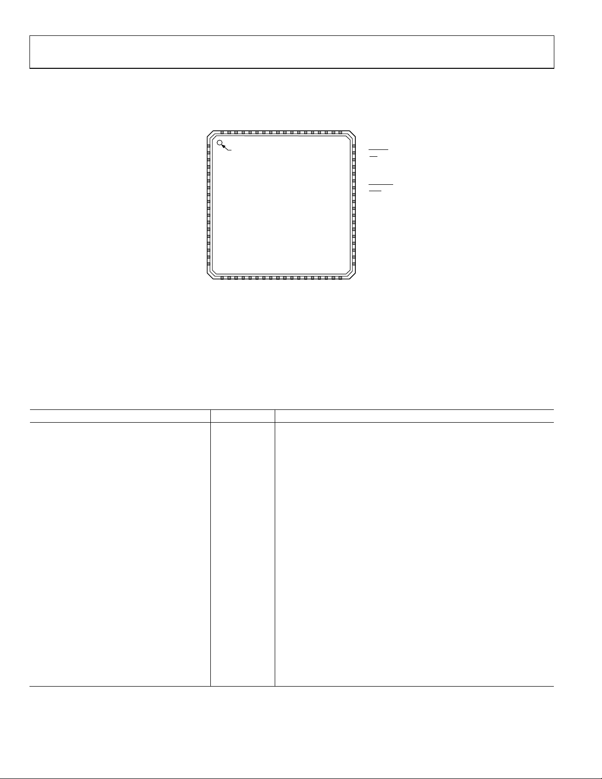
72-lead LFCSP (10 mm × 10 mm)
APPLICATIONS
Routing of high speed signals including
Video (NTSC, PAL, S, SECAM, YUV, RGB)
Compressed video (MPEG, wavelet)
3-level digital video (HDB3)
Data communications
Telecommunications
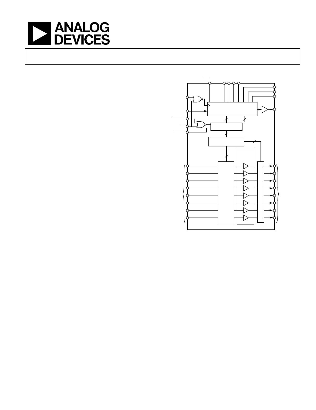
CLK
DATAIN
UPDATE
RESET
8
ADV3228/ADV3229
FUNCTIONAL BLOCK DIAGRAM
CE
INPUTS
SER/PAR
ADV3228/
ADV3229
D0 D1 D2 D3
40-BIT SHIFT REGISTER
WITH 4-BIT
PARALLEL LOADING
32 8
PARALLEL LATCH
32
DECODE
8 × 4:8 DECODERS
OUTPUT
BUFFER
64
SWITCH
Figure 1.
(RESERVED)
SET INDIVIDUAL
OR RESET ALL
OUTPUTS TO OFF
8
G = +1,
G = +2
Switch
A0
A1
A2
DATAOUT
8
ENABLED/DISABLED
OUTPUTS
09318-001
GENERAL DESCRIPTION
The ADV3228/ADV3229 are high speed 8 × 8 analog crosspoint
switch matrices. They offer a −3 dB large signal bandwidth of
750 MHz (ADV3228) and a slew rate of 2500 V/µs.
The ADV3228/ADV3229 include eight independent output buffers
that can be placed into a high impedance state for paralleling
crosspoint outputs to prevent off channels from loading the output
bus. The ADV3228 has a gain of +1, the ADV3229 has a gain of
+2, and they both operate on voltage supplies of ±5 V. Channel
Rev. 0
Information furnished by Analog Devices is believed to be accurate and reliable. However, no
responsibility is assumed by Analog Devices for its use, nor for any infringements of patents or other
rights of third parties that may result from its use. Specifications subject to change without notice. No
license is granted by implication or otherwise under any patent or patent rights of Analog Devices.
Trademarks and registered trademarks are the property of their respective owners.
switching is performed via a serial digital control that can
accommodate daisy chaining of several devices or via a parallel
control to allow updating of an individual output without
reprogramming the entire array.
The ADV3228/ADV3229 are available in the 72-lead LFCSP
package over the extended industrial temperature range of
−40°C to +85°C.
One Technology Way, P.O. Box 9106, Norwood, MA 02062-9106, U.S.A.
Tel: 781.329.4700 www.analog.com
Fax: 781.461.3113 ©2010 Analog Devices, Inc. All rights reserved.
Page 2

ADV3228/ADV3229
TABLE OF CONTENTS
Features .............................................................................................. 1
Applications ....................................................................................... 1
Functional Block Diagram .............................................................. 1
General Description ......................................................................... 1
Revision History ............................................................................... 2
Specifications ..................................................................................... 3
Timing Characteristics (Serial) .................................................. 5
Logic Levels ................................................................................... 5
Timing Characteristics (Parallel) ............................................... 6
Absolute Maximum Ratings ............................................................ 7
Thermal Resistance ...................................................................... 7
Power Dissipation ......................................................................... 7
ESD Caution .................................................................................. 7
REVISION HISTORY
11/10—Revision 0: Initial Version
Pin Configuration and Function Descriptions ..............................8
Truth Table and Logic Diagram ............................................... 10
Typical Performance Characteristics ........................................... 11
Circuit Diagrams ............................................................................ 20
Theory of Operation ...................................................................... 21
Applications Information .............................................................. 22
Serial Programming ................................................................... 22
Parallel Programming ................................................................ 22
Power-On Reset .......................................................................... 23
Gain Selection ............................................................................. 23
Creating Larger Crosspoint Arrays .......................................... 23
Outline Dimensions ....................................................................... 24
Ordering Guide .......................................................................... 24
Rev. 0 | Page 2 of 24
Page 3

ADV3228/ADV3229
SPECIFICATIONS
VS = ±5 V, TA = 25°C, RL = 150 Ω, unless otherwise noted.
Table 1.
ADV3228 ADV3229
Parameter Test Conditions/Comments Min Typ Max Min Typ Max Unit
DYNAMIC PERFORMANCE
−3 dB Bandwidth 200 mV p-p 1200 900 MHz
2 V p-p 750 850 MHz
Gain Flatness 0.1 dB, 2 V p-p 55 50 MHz
0.5 dB, 2 V p-p 250 235 MHz
Propagation Delay 2 V p-p 0.6 0.6 ns
Settling Time 1%, 2 V step 3 3 ns
Slew Rate 2 V step, peak 2500 2500 V/μs
NOISE/DISTORTION PERFORMANCE
Differential Gain Error NTSC or PAL 0.01 0.02 %
Differential Phase Error NTSC or PAL 0.01 0.02 Degrees
Crosstalk, All Hostile, RTO f = 100 MHz −45 −45 dB
f = 5 MHz −87 −70 dB
Off Isolation, Input to Output f = 100 MHz, one channel −80 −87 dB
OIP2 f = 100 MHz, RL = 100 Ω 38 dBm
f = 500 MHz, RL = 100 Ω 15 dBm
OIP3 f = 100 MHz, RL = 100 Ω 32 dBm
f = 500 MHz, RL = 100 Ω 7 dBm
Output 1 dB Compression Point f = 100 MHz, RL = 100 Ω 19 dBm
f = 500 MHz, RL = 100 Ω 10 dBm
Input Voltage Noise Density 50 MHz 18 18 nV/√Hz
DC PERFORMANCE
Gain Error 0.1 0.5 0.2 1.5 %
Gain Matching Channel-to-channel 0.5 1.5 %
Gain Temperature Coefficient 0.5 5 ppm/°C
OUTPUT CHARACTERISTICS
Output Resistance DC, enabled 0.2 0.2 Ω
DC, disabled 15 8 MΩ
Output Disabled Capacitance 2.2 2.6 pF
Output Leakage Current Output disabled 0.5 0.5 μA
Output Voltage Range No load ±3 ±3 V
R
Short-Circuit Current 55 55 mA
INPUT CHARACTERISTICS
Input Offset Voltage Worst case (all configurations) ±5 ±5 mV
Input Offset Voltage Drift 5 5 μV/°C
Input Voltage Range ±3 ±1.5 V
Input Capacitance Any switch configuration 1.8 1.8 pF
Input Resistance 2 2 MΩ
Input Bias Current Any switch configuration ±1 ±1 μA
SWITCHING CHARACTERISTICS
Enable/Disable Time
Switching Time, 2 V Step
Switching Transient (Glitch) 25 50 mV p-p
= 150 Ω ±2.8 ±2.8 V
L
50% UPDATE
50% UPDATE
to 1% settling
to 1% settling
20 20 ns
20 20 ns
Rev. 0 | Page 3 of 24
Page 4

ADV3228/ADV3229
ADV3228 ADV3229
Parameter Test Conditions/Comments Min Typ Max Min Typ Max Unit
POWER SUPPLIES
Supply Current AVCC, outputs enabled, no load 52 70 58 70 mA
AVCC, outputs disabled 12 18 13 18 mA
AVEE, outputs enabled, no load 52 70 58 70 mA
AVEE, outputs disabled 12 18 14 18 mA
DVCC, outputs enabled, no load 6 6 mA
Supply Voltage Range ±4.5 ±5 ±5.5 ±4.5 ±5 ±5.5 V
PSRR DC to 50 kHz, AVCC, AVEE <−60 <−60 dB
f = 100 kHz, AVCC, AVEE −60 −60 dB
f = 10 MHz, AVCC −48 −35 dB
f = 10 MHz, AVEE −35 −55 dB
f = 100 MHz, AVCC −25 −15 dB
f = 100 MHz, AVEE −15 −15 dB
f = 100 kHz, DVCC −90 −90 dB
OPERATING TEMPERATURE RANGE
Temperature Range Operating (still air) −40 +85 −40 +85 °C
θJA Operating (still air) 29 29 °C/W
Rev. 0 | Page 4 of 24
Page 5
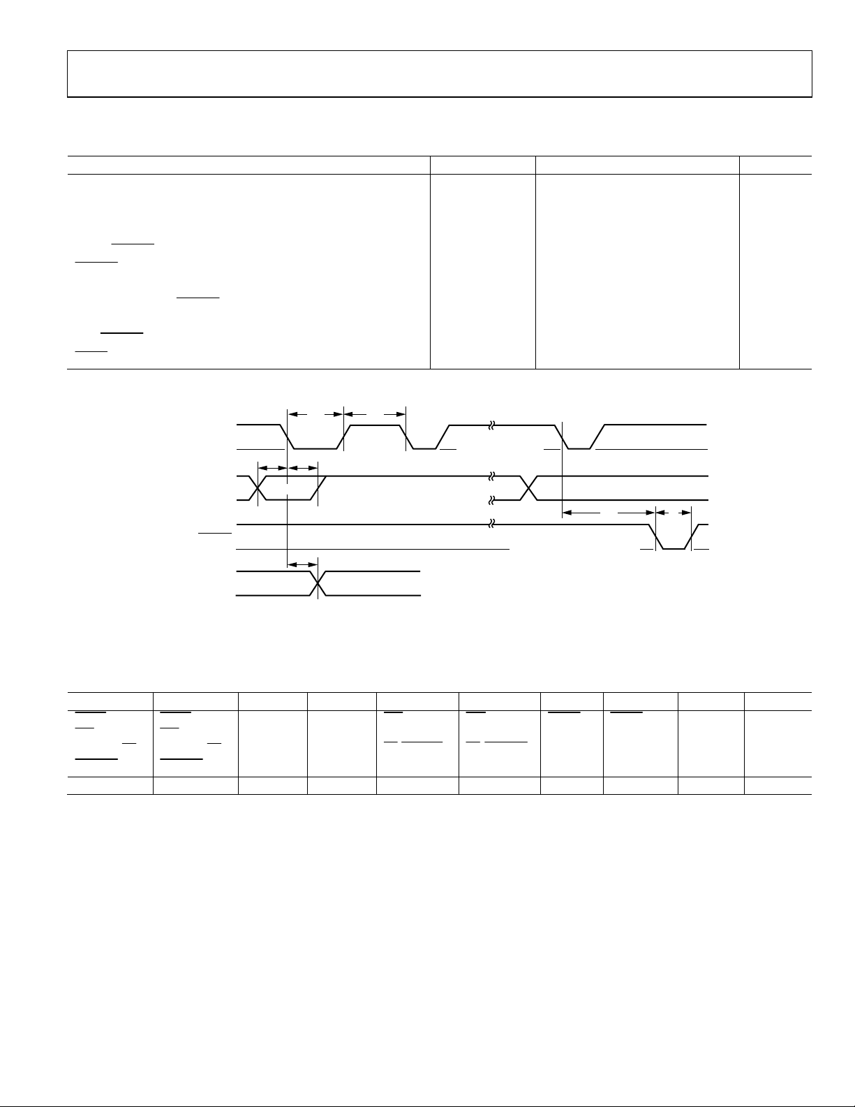
ADV3228/ADV3229
0
TIMING CHARACTERISTICS (SERIAL)
Table 2.
Parameter Symbol Min Typ Max Unit
Serial Data Setup Time t1 10 ns
CLK Pulse Width t2 10 ns
Serial Data Hold Time t3 10 ns
CLK Pulse Separation, Serial Mode t4 10 ns
t
CLK to UPDATE Delay
UPDATE Pulse Width
CLK to DATAOUT Valid, Serial Mode t7 50 ns
Propagation Delay, UPDATE to Switch On or Off
Data Load Time, CLK = 5 MHz, Serial Mode 8 μs
CLK, UPDATE Rise and Fall Times
RESET Time
Timing Diagram—Serial Mode
CLK
DATAIN
1 = LATCHED
UPDATE
= TRANSPARENT
t
1
0
1
0
t1t
OUT07 (D3) OUT07 (RESERVED) OUT00 (D0)
2
3
t
7
t
4
10 ns
5
t
10 ns
6
20 ns
50 ns
30 ns
LOAD DATA INT O
SERIAL REGI STER
ON FALLING EDGE
t
5
TRANSFER DATA FROM SERIAL
REGISTE R T O PARALLEL
LATCHES DURING LOW LEVEL
t
6
DATAOUT
09318-002
Figure 2. Timing Diagram, Serial Mode
LOGIC LEVELS
Table 3. Logic Levels
VIH V
RESET,
/PAR, CLK,
SER
DATA IN, CE
UPDATE
2.0 V min 0.8 V max 2.4 V min 0.4 V max 2 μA max 2 μA max 2 μA max 300 μA max 3 mA min 1 mA min
V
IL
RESET
,
/PAR, CLK,
SER
,
DATA IN, CE
UPDATE
,
V
OH
I
OL
DATA OUT DATA OUT
I
IH
/PAR,
SER
CLK, DATA IN,
CE
, UPDATE
I
IL
/PAR,
SER
CLK, DATA IN,
CE
, UPDATE
I
IH
RESET
I
IL
RESET
I
OH
OL
DATA OUT DATA OUT
Rev. 0 | Page 5 of 24
Page 6
ADV3228/ADV3229
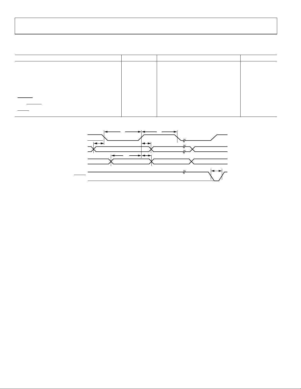
TIMING CHARACTERISTICS (PARALLEL)
Table 4.
Parameter Symbol Min Typ Max Unit
Parallel Data Setup Time t1d 10 ns
Address Setup Time t1a 10 ns
CLK Pulse Width t2 10 ns
Parallel Data Hold Time t3d 10 ns
Address Hold Time t3a 10 ns
CLK Pulse Separation t4 20 ns
t
UPDATE Pulse Width
CLK, UPDATE Rise and Fall Times
RESET Time
Timing Diagram—Parallel Mode
CLK
A0 TO A2
D0 TO D3
1 = LATCHED
UPDATE
0 = TRANSPARENT
1
0
1
0
1
0
t
1a
10 ns
5
50 ns
30 ns
t
2
t
1d
Figure 3. Timing Diagram, Parallel Mode
t
4
t
3a
t
3d
t
5
09318-003
Rev. 0 | Page 6 of 24
Page 7
ADV3228/ADV3229
ABSOLUTE MAXIMUM RATINGS
Table 5.
Parameter Rating
Analog Supply Voltage (AVCC to AVEE) 11 V
Digital Supply Voltage (DVCC to DGND) 6 V
Supply Potential Difference (AVCC to DVCC) ±0.5 V
Ground Potential Difference
±0.5 V
(AGND to DGND)
Maximum Potential Difference
6 V
(DVCC to AVEE)
Analog Input Voltage AVEE < VIN < AVCC
Digital Input Voltage DGND < DIN < DVCC
Exposed Paddle Voltage AGND
Output Voltage (Disabled Analog Output) AVEE < V
< AVCC
OUT
Output Short-Circuit
Duration Momentary
Current
Internally limited
to 55 mA
Temperature
Storage Temperature Range −65°C to +125°C
Operating Temperature Range −40°C to +85°C
Junction Temperature 150°C
Lead Temperature
300°C
(Soldering, 10 sec)
Stresses above those listed under Absolute Maximum Ratings
may cause permanent damage to the device. This is a stress
rating only; functional operation of the device at these or any
other conditions above those indicated in the operational
section of this specification is not implied. Exposure to absolute
maximum rating conditions for extended periods may affect
device reliability.
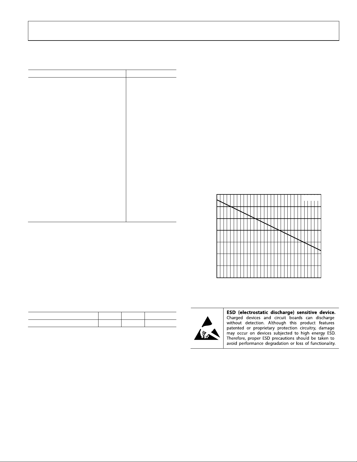
THERMAL RESISTANCE
θJA is specified for the worst-case conditions, that is, a device
soldered in a circuit board for surface-mount packages.
Table 6. Thermal Resistance
Package Type θJA θ
72-Lead LFCSP_VQ 29 0.5 °C/W
Unit
JC
POWER DISSIPATION
The ADV3228/ADV3229 operate with ±5 V supplies and can
drive loads down to 100 Ω, resulting in a wide range of possible
power dissipations. For this reason, extra care must be taken when
derating the operating conditions based on ambient temperature.
Packaged in the 72-lead LFCSP, the ADV3228/ADV3229 junctionto-ambient thermal impedance (θ
) is 29°C/W. For long-term
JA
reliability, the maximum allowed junction temperature of the
die should not exceed 125°C; even temporarily exceeding this
limit can cause a shift in parametric performance due to a change
in stresses exerted on the die by the package. Exceeding a junction
temperature of 150°C for an extended period can result in device
failure. In Figure 4, the curve shows the range of allowed internal
die power dissipation that meets these conditions over the −40°C
to +85°C ambient temperature range. When using Figure 4, do
not include the external load power in the maximum power
calculation, but do include the load current dropped on the die
output transistors.
7
6
5
4
3
2
MAXIMUM PO WER DISSIPATION (W)
1
0
–40 –20 0 20 40 60 80
AMBIENT TEMPERATURE (°C)
Figure 4. Maximum Die Power Dissipation vs. Ambient Temperature
T
= 150°C
J
9318-004
ESD CAUTION
Rev. 0 | Page 7 of 24
Page 8
ADV3228/ADV3229
2
F
L
PIN CONFIGURATION AND FUNCTION DESCRIPTIONS
AGNDNCAVEENCAVCCNCAVEE
7271706968676665646362616059585756
AVCC
1
IN0
2
AVEE
3
IN1
4
AVCC
5
IN2
6
AVEE
7
IN3
8
AVCC
9
10
IN4
11
AVEE
12
IN5
13
AVCC
14
IN6
15
AVEE
16
IN7
17
AGND
18
AVEE
NOTES
1. NC = NO CONNECT. DO NOT CONNECT TO THIS PIN.
. EXPOSED PADDLE. THE EXPOSED METAL PADDLE ON THE BOTTOM O
THE LFCSP PACKAGE MUST BE SOLDERED TO THE PCB AGND FOR
PROPER HEAT DISSIPATI ON AND FOR NOI S E AND M E CHANI CA
STRENGTH BENEFITS.
PIN 1
INDICATOR
ADV3228/ADV3229
1920212223242526272829303132333435
OUT7
OUT6
AVEE
AVCC
AVCCNCAVEENCAVCCNCAVEENCAGND
NC
TOP VIEW
(Not to S cale)
OUT4
OUT5
AVEE
AVCC
AVCC
DVCC
55
54
DGND
53
RESET
52
CE
51
DATAOUT
50
CLK
49
DATAIN
48
UPDATE
47
SER/PAR
46
A0
45
A1
44
A2
43
D0
42
D1
41
D2
40
D3
39
NC
38
DGND
37
DVCC
36
OUT3
OUT2
OUT1
AVEE
OUT0
AVEE
AVCC
AVEE
AVCC
09318-005
Figure 5. Pin Configuration
Table 7. Pin Function Descriptions
Pin No. Mnemonic Description
1, 5, 9, 13, 19, 23, 27, 31, 35, 60, 64, 68 AVCC Analog Positive Supply.
2 IN0 Input Number 0.
3, 7, 11, 15, 18, 21, 25, 29, 33, 36, 58, 62, 66, 70 AVEE Analog Negative Supply.
4 IN1 Input Number 1.
6 IN2 Input Number 2.
8 IN3 Input Number 3.
10 IN4 Input Number 4.
12 IN5 Input Number 5.
14 IN6 Input Number 6.
16 IN7 Input Number 7.
17, 56, 72 AGND Analog Ground.
20 OUT7 Output Number 7.
22 OUT6 Output Number 6.
24 OUT5 Output Number 5.
26 OUT4 Output Number 4.
28 OUT3 Output Number 3.
30 OUT2 Output Number 2.
32 OUT1 Output Number 1.
34 OUT0 Output Number 0.
37, 55 DVCC Digital Positive Supply.
38, 54 DGND Digital Ground.
39, 57, 59, 61, 63, 65, 67, 69, 71 NC No Internal Connection.
Rev. 0 | Page 8 of 24
Page 9

ADV3228/ADV3229
Pin No. Mnemonic Description
40 to 43 D3, D2, D1, D0 Parallel Data Input.
44 to 46 A2, A1, A0 Parallel Output Address Input.
47
48
49 DATAIN Serial Data In (Control Pin).
50 CLK Serial Data Clock, Parallel First Rank Latch Enable (Control Pin).
51 DATAOUT Serial Data Out.
52
53
EPAD
/PAR
SER
UPDATE
CE
RESET
Serial/Parallel Mode Select (Control Pin).
Second Rank Write Strobe (Control Pin).
Chip Enable (Control Pin).
Second Rank Reset (Control Pin).
Exposed Paddle. The exposed metal paddle on the bottom of the LFCSP
package must be soldered to the PCB AGND for proper heat dissipation
and for noise and mechanical strength benefits.
Rev. 0 | Page 9 of 24
Page 10

ADV3228/ADV3229
TRUTH TABLE AND LOGIC DIAGRAM
Table 8. Operation Truth Table1
CE
UPDATE
CLK DATAIN DATAOUT
RESET
1 X X X X X X No change in logic.
0 X
0 X 0 D0…D3
Data
2
Data
I
Not applicable in
X 0
I-80
X 1
parallel mode3
0 0 X X X 1 X
X X X X X 0 X
1
X is don’t care.
2
DataI: serial data. Reserved bit internally set to Logic 1.
3
DATAOUT remains active in parallel mode and always reflects the state of the MSB of the serial shift register.
DATA
D0
D1
D2
D3
D
CLK
S
D1
Q
Q
D0
S
D1
Q
D0
D
CLK
S
D1
Q
Q
D0
D
CLK
S
D1
Q
Q
D0
D
CLK
S
D1
Q
Q
D0
D
CLK
S
D1
Q
D
Q
D0
CLK
PARALLEL
RESERVED
(INTERNALLY
SET HIGHT)
(OUTPUT
ENABLE)
SER/PAR
DATAIN
(SERIAL)
SER
Q
/PAR
S
D1
Q
D0
Description
The data on the serial DATAIN line is loaded into the
serial register. The first bit clocked into the serial
register appears at DATAOUT 40 clock cycles later.
The data on the parallel data lines, D0 to D3, are
loaded into the 40-bit serial shift register location
addressed at A0 to A2.
Data in the 40-bit shift register transfers into the
parallel latches that control the switch array. Latches
are transparent.
Asynchronous operation. All outputs are disabled.
Second rank latches are cleared. Remainder of logic
is unchanged.
D
CLK
S
D1
Q
Q
D0
D
CLK
S
D1
D
Q
Q
Q
D0
CLK
D
CLK
S
D1
Q
Q
D0
S
D1
Q
D0
D
CLK
S
D1
Q
D0
DATA
Q
D
Q
OUT
CLK
CLK
CE
UPDATE
OUT0 EN
OUT1 EN
OUT2 EN
OUTPUT
ADDRESS
OUT3 EN
OUT4 EN
A0
OUT5 EN
A1
3 TO 8 DECODER
OUT6 EN
A2
OUT7 EN
(OUTPUT ENABLE)
RESET
LE
OUT0
D
B0
Q
LE
OUT0
B1
D
Q
LE
OUT0
B2
D
Q
LE
OUT0
R
D
Q
LE
OUT0
EN
D
QCLR
LE
OUT1
D
B0
Q
LE
OUT6
EN
D
QCLR
LE
OUT7
B0
D
Q
LE
OUT7
B1
D
Q
LE
OUT7
B2
D
Q
LE
OUT7
R
D
Q
LE
OUT7
EN
D
QCLR
DECODE
128
8
OUTPUT ENABL ESWITCH MATRIX
09318-006
Figure 6. Logic Diagram
Rev. 0 | Page 10 of 24
Page 11

ADV3228/ADV3229
TYPICAL PERFORMANCE CHARACTERISTICS
4
OUTPUT SI GNAL, UNICAST
3
OUTPUT SI GNAL, BROADCAST
2
1
0
–1
–2
–3
–4
–5
GAIN (dB)
–6
–7
–8
–9
–10
–11
V
= 200mV p-p
OUT
–12
1 10 100 1000 10000
FREQUENCY ( MHz )
Figure 7. ADV3228 Small Signal Frequency Response
4
OUTPUT SIGNAL, UNICAS T
3
OUTPUT SIGNAL, BROADCAS T
2
1
0
–1
–2
–3
–4
–5
GAIN (dB)
–6
–7
–8
–9
–10
–11
V
= 2V p-p
OUT
–12
1 10 100 1000 10000
FREQUENCY (M Hz)
Figure 8. ADV3228 Large Signal Frequency Response
6
5
4
3
2
1
0
–1
–2
–3
GAIN (dB)
–4
–5
–6
–7
–8
–9
V
= 200mV p-p
OUT
–10
1 10 100 1000 10000
10.4pF
1.2pF
0pF
FREQUENCY (MHz )
5.2pF
2.2pF
Figure 9. ADV3228 Small Signal Frequency Response with Capacitive Loads
09318-008
09318-009
09318-010
10
OUTPUT SIGNAL, UNICAST
9
OUTPUT SIGNAL, BROADCAST
8
7
6
5
4
3
2
1
0
–1
GAIN (dB)
–2
–3
–4
–5
–6
–7
–8
–9
V
= 200mV p-p
OUT
–10
1 10 100 1000 10000
FREQUENCY (MHz)
Figure 10. ADV3229 Small Signal Frequency Response
10
OUTPUT SI GNAL, UNICAST
9
OUTPUT SI GNAL, BROADCAST
8
7
6
5
4
3
2
1
0
–1
GAIN (dB)
–2
–3
–4
–5
–6
–7
–8
–9
V
= 2V p-p
OUT
–10
1 10 100 1000 10000
FREQUENCY (MHz)
Figure 11. ADV3229 Large Signal Frequency Response
14
13
12
11
10
9
8
7
6
5
4
3
2
1
0
GAIN (dB)
–1
–2
–3
–4
–5
–6
–7
–8
–9
V
= 200mV p-p
OUT
–10
1 10 100 1000 10000
10.4pF
1.2pF
0pF
FREQUENCY ( M Hz )
5.2pF
2.2pF
Figure 12. ADV3229 Small Signal Frequency Response, RL = 150 Ω
09318-011
09318-012
09318-013
Rev. 0 | Page 11 of 24
Page 12

ADV3228/ADV3229
4
3
2
1
0
–1
–2
–3
–4
GAIN (dB)
–5
–6
–7
–8
–9
V
= 2V p-p
OUT
–10
1 10 100 1000 10000
10.4pF
1.2pF
0pF
FREQUENCY ( MHz )
5.2pF
2.2pF
09318-014
Figure 13. ADV3228 Large Signal Frequency Response with Capacitive Loads
0.15
INPUT SIGNAL
OUTPUT SI GNAL, UNICAST
OUTPUT SI GNAL, BROADCAST
0.10
0.05
(V)
0
OUT
V
–0.05
14
13
12
11
10
9
8
7
6
5
4
3
2
1
0
GAIN (dB)
–1
–2
–3
–4
–5
–6
–7
–8
V
= 2V p-p
–9
OUT
–10
1 10 100 1000 10000
10.4pF
2.2pF
1.2pF
FREQUENCY ( MHz)
0pF
5.2pF
09318-017
Figure 16. ADV3229 Large Signal Frequency Response with Capacitive Loads
0.15
INPUT
OUTPUT SI GNAL, UNICAST
OUTPUT SI GNAL, BROADCAST
0.10
0.05
(V)
0
OUT
V
–0.05
–0.10
V
= 200mV p-p
OUT
–0.15
0 2 4 6 8 10 12 14 16 18 20
TIME (ns)
09318-015
Figure 14. ADV3228 Small Signal Pulse Response
0.15
INPUT SIGNAL
OUTPUT SI GNAL, UNICAST
OUTPUT SI GNAL, BROADCAST
0.10
0.05
(V)
0
OUT
V
–0.05
–0.10
V
= 2V p-p
OUT
–0.15
0 2 4 6 8 101214161820
Time (ns)
09318-016
Figure 15. ADV3228 Large Signal Pulse Response
–0.10
V
= 200mV p-p
OUT
–0.15
0 2 4 6 8 101214161820
TIME (ns)
09318-018
Figure 17. ADV3229 Small Signal Pulse Response
1.5
INPUT
OUTPUT SIGNAL, UNICAST
OUTPUT SIGNAL, BROADCAS T
1.0
0.5
(V)
0
OUT
V
–0.5
–1.0
V
= 2V p-p
OUT
–1.5
0 2 4 6 8 101214161820
TIME (ns)
09318-019
Figure 18. ADV3229 Large Signal Pulse Response
Rev. 0 | Page 12 of 24
Page 13

ADV3228/ADV3229
2.0
RISING EDGE PULSE
RISING EDGE SLEW RATE
1.5
1.0
0.5
(V)
0
OUT
V
–0.5
–1.0
–1.5
–2.0
0 0.5 1.0 1.5 2.0 2.5 3.0 3.5 4.0 4.5 5.0
TIME (ns)
Figure 19. ADV3228 Rising Edge Slew Rate
2.0
1.5
1.0
0.5
(V)
0
OUT
V
–0.5
–1.0
–1.5
FALLING EDGE PULSE
FALLING EDGE SLEW RATE
–2.0
0 0.5 1.0 1.5 2.0 2.5 3.0 3.5 4.0 4.5 5.0
TIME (ns)
Figure 20. ADV3228 Falling Edge Slew Rate
1.5
1.0
0.5
(V)
OUT
V
–0.5
OUTPUT–INPUT
0
INPUT SIGNAL
OUTPUT SIGNAL
3000
2500
2000
1500
1000
500
0
–500
–1000
500
0
–500
–1000
–1500
–2000
–2500
–3000
–3500
40
30
20
10
0
2.0
1.5
1.0
0.5
(V)
0
OUT
V
SLEW RATE (V/μs)
09318-020
–0.5
–1.0
–1.5
RISING E DGE PULS E
RISING EDGE SLEW RATE
–2.0
0 0.5 1.0 1.5 2.0 2.5 3.0 3.5 4.0 4.5 5.0
TIME (ns)
Figure 22. ADV3229 Rising Edge Slew Rate
2.0
FALLING EDGE PULSE
FALLING EDGE SLEW RATE
1.5
1.0
0.5
(V)
0
OUT
V
SLEW RATE (V/μs)
09318-021
–0.5
–1.0
–1.5
–2.0
0 0.5 1.0 1.5 2.0 2.5 3.0 3.5 4.0 4.5 5.0
TIME (ns)
Figure 23. ADV3229 Falling Edge Slew Rate
1.5
OUTPUT–INPUT
1.0
0.5
(V)
0
OUT
V
OUTPUT ERRO R ( %)
–0.5
INPUT SIGNAL
OUTPUT SIGNAL
4000
3500
3000
2500
2000
1500
1000
500
0
–500
–1000
1000
500
0
–500
–1000
–1500
–2000
–2500
–3000
–3500
–4000
40
30
20
10
0
SLEW RATE (V/μs)
SLEW RATE (V/μs)
OUTPUT ERRO R (%)
09318-022
09318-023
–1.0
–1.5
–2.0 –1.5 –1.0 –0.5 0 0.5 1.0 1.5 2.0 3.02.5
PROPAGATI ON DELAY NOT SHOWN
TIME (ns)
Figure 21. ADV3228 Settling Time
–10
–20
09318-049
Rev. 0 | Page 13 of 24
–1.0
–1.5
–1.0 –0.5 0 0.5 1.0 1.5 2.0 2.5 3.0 3.5 4.0
PROPAGATI ON DELAY NOT SHOWN
TIME (ns)
Figure 24. ADV3229 Settling Time
–10
–20
09318-050
Page 14

ADV3228/ADV3229
–
L
A
–
L
A
20
10
0
–10
–20
–30
–40
PSR (dB)
–50
–60
–70
–80
–90
0.1 1 10
FREQUENCY (M Hz)
VEE AGGRESSOR
VCC AGGRESSOR
100 1k
09318-051
Figure 25. ADV3228 Power Supply Rejection
400
350
300
250
200
150
NOISE (nV/√Hz)
100
50
0
1 10 100 1000 10000 100000
FREQUENCY ( kHz)
09318-024
Figure 26. ADV3228 Output Noise, 100 Ω Load
40
20
10
0
–10
–20
–30
–40
PSR (dB)
–50
–60
–70
–80
–90
0.1 1 10
VCC AGGRESSOR
VEE AGGRESSOR
FREQUENCY (M Hz )
100 1k
09318-052
Figure 28. ADV3229 Power Supply Rejection
700
650
600
550
500
450
400
350
300
NOISE (n V/Hz)
250
200
150
100
50
0
1 10 100 1000 10000 100000
FREQUENCY (kHz )
09318-026
Figure 29. ADV3229 Output Noise, 100 Ω Load
20
–50
–60
–70
–80
TION (dB)
–90
ISO
–100
–110
–120
1 10 100 1000
FREQUENCY ( MHz)
Figure 27. ADV3228 Off Isolation
09318-025
–40
–60
–80
TION (dB)
ISO
–100
–120
–140
1 10 100 1000
FREQUENCY ( MHz )
Figure 30. ADV3229 Off Isolation
09318-027
Rev. 0 | Page 14 of 24
Page 15

ADV3228/ADV3229
0
IN11-OUT3: V ICTIM CHANNEL
IN12-OUT4: AGGRESSOR
–10
V
= 2V p-p
OUT
–20
–30
–40
–50
–60
–70
CROSSTALK (dB)
–80
–90
–100
–110
1 10 100 1000
FREQUENCY ( M Hz )
Figure 31. ADV3228 Crosstalk, One Adjacent Channel, RTO
0
IN3-OUT3: VI CTIM CHANNEL
V
= 2V p-p
–10
OUT
–20
–30
–40
–50
–60
–70
CROSSTALK (dB)
–80
–90
–100
–110
1 10 100 1000
FREQUENCY ( M Hz )
Figure 32. ADV3228 Crosstalk, All Hostile, RTO
1M
09318-029
09318-030
0
IN11-OUT3:V ICTIM CHANNEL
IN12-OUT4: AGGRESSOR
–10
V
= 2V p-p
OUT
–20
–30
–40
–50
–60
–70
CROSSTALK (dB)
–80
–90
–100
–110
1 10 100 1000
FREQUENCY ( M Hz )
Figure 34. ADV3229 Crosstalk, One Adjacent Channel, RTO
20
IN3-OUT3: VICTIM CHANNEL
10
V
= 2V p-p
OUT
0
–10
–20
–30
–40
–50
–60
CROSSTALK (dB)
–70
–80
–90
–100
–110
1 10 100 1000
FREQUENCY ( MHz)
Figure 35. ADV3229 Crosstalk, All Hostile, RTO
1M
09318-032
09318-033
100k
10k
1k
IMPEDANCE (Ω)
100
10
1
0.1 1 10
100
FREQUENCY ( M Hz )
1000 10000
Figure 33. ADV3228 Input Impedance
09318-031
Rev. 0 | Page 15 of 24
100k
10k
1k
IMPEDANCE (Ω)
100
10
1
0.1 1 10 100 1000 10000
FREQUENCY ( M Hz )
Figure 36. ADV3229 Input Impedance
09318-034
Page 16

ADV3228/ADV3229
1M
1M
100k
10k
1k
IMPEDANCE (Ω)
100
10
1
0.1 1 10 100 1000
FREQUENCY ( M Hz )
09318-035
Figure 37. ADV3228 Output Impedance, Disabled
100
10
IMPEDANCE (Ω)
1
100k
10k
1k
IMPEDANCE (Ω)
100
10
1
0.1 1 10 100 1000
FREQUENCY ( M Hz )
09318-038
Figure 40. ADV3229 Output Impedance, Disabled
100
10
IMPEDANCE (Ω)
1
0.1
0.1 1 10 100 1000
FREQUENCY ( M Hz )
Figure 38. ADV3228 Output Impedance, Enabled
2.0
1.5
1.0
0.5
(V)
0
OUT
V
–0.5
–1.0
–1.5
–2.0
–20 –15 –10 –5 0 5 10 15 20 25 30
UPDATE
TIME (ns)
V
OUT
V
FALLING EDGE
OUT
Figure 39. ADV3228 Switching Time
RISING EDGE
3.5
3.0
2.5
2.0
1.5
1.0
0.5
0
–0.5
0.1
0.1 1 10 100 1000
09318-036
FREQUENCY ( M Hz )
09318-039
Figure 41. ADV3229 Output Impedance, Enabled
2.0
UPDATE
1.5
V
RISING EDGE
1.0
0.5
(V)
0
OUT
UPDATE (V)
09318-037
V
–0.5
–1.0
–1.5
–2.0
–20 –15 –10 –5 0 5 10 15 20 25 30
TIME (ns)
OUT
V
FALLING EDGE
OUT
Figure 42. ADV3229 Switching Time
3.5
3.0
2.5
2.0
1.5
1.0
0.5
0
–0.5
UPDATE (V )
09318-040
Rev. 0 | Page 16 of 24
Page 17

ADV3228/ADV3229
A
0.0500
0.0375
0.0250
0.0125
(V)
OUT
V
–0.0125
–0.0250
–0.0375
–0.0500
UPDATE
V
OUT
0
–15 –10 –5 0 5 10 15 20
TIME (ns)
Figure 43. ADV3228 Switching Glitch
4
UPDATE
3
2
1
(V)
0
OUT
V
1
2
3
4
–20 –15 –10 –5 0 5 10 15 20 25 30
TIME (ns)
V
OUT
FALLING EDGE
V
OUT
Figure 44. ADV3228 Enable Time
0.0045
0.0040
0.0035
0.0030
0.0025
0.0020
0.0015
0.0010
0.0005
DIFFERENT IAL GAIN ERROR (%)
0
–0.0005
–0.8 –0.6 –0.4 –0.2 0 0.2 0.4 0.6 0.8
INPUT DC OFFSET (V)
Figure 45. ADV3228 Differential Gain Error
RISING EDG E
3.5
3.0
2.5
2.0
1.5
UPDATE (V)
1.0
0.5
0
–0.5
30
25
09318-041
0.100
0.075
0.050
0.025
(V)
0
OUT
V
–0.025
–0.050
–0.075
–0.100
–15 –10 –5 0 5 10
UPDATE
TIME (ns)
V
OUT
15
20 25 30
3.5
3.0
2.5
2.0
1.5
1.0
0.5
0
–0.5
UPDATE (V)
Figure 46. ADV3229 Switching Glitch
3.5
3.0
2.5
2.0
1.5
1.0
0.5
0
0.5
UPDATE (V)
09318-042
4
3
2
1
(V)
0
OUT
V
–1
–2
–3
–4
–20 –15 –10 –5 0 5 10 15 20 25 30
UPDATE
TIME (ns)
V
RISING EDGE
OUT
FALLING EDGE
V
OUT
Figure 47. ADV3229 Enable Time
3.5
3.0
2.5
2.0
1.5
1.0
0.5
0
–0.5
UPDATE (V)
0.014
0.012
0.010
0.008
L GAIN ERROR (%)
0.006
0.004
DIFFERENTI
0.002
0
09318-043
–0.7 –0.6 –0.5 –0.4 –0.3 –0.2 –0.1 0 0.1 0.2 0.3 0.4 0.5 0.6 0.7
INPUT DC OFFSET (V)
09318-046
Figure 48. ADV3229 Differential Gain Error
09318-044
09318-045
Rev. 0 | Page 17 of 24
Page 18

ADV3228/ADV3229
T
T
0.001
0.002
0
–0.001
–0.002
–0.003
–0.004
–0.005
–0.006
DIFFERENTIAL PHASE E RROR (Degrees)
–0.007
–0.7 –0.6 –0.5 –0.4 –0.3 –0.2 –0.1 0 0.1 0.2 0.3 0.4 0.5 0.6 0.7
INPUT VOLTAGE (V)
09318-047
Figure 49. ADV3228 Differential Phase Error
5
4
3
2
1
0
AGE (V)
–1
VOL
–2
–3
–4
–5
0 102030405060708090100
VIN = 8.5V p- p
V
AT VIN = 8.5V p-p
OUT
TIME (ns)
09318-053
Figure 50. ADV3228 Overdrive Recovery
22
REF: 50Ω
20
18
0
–0.002
–0.004
–0.006
–0.008
–0.010
–0.012
DIFFERENTIAL PHASE ERROR (Degrees)
–0.014
–0.7 –0.6 –0.5 –0.4 –0.3 –0.2 –0.1 0 0.1 0.2 0.3 0.4 0.5 0.6 0.7
INPUT VOLTAGE (V)
Figure 52. ADV3229 Differential Phase Error
5
4
3
2
1
0
AGE (V)
–1
VOL
–2
–3
–4
–5
0 102030405060708090100
V
AT VIN = 8.5V p-p
OUT
TIME (ns)
VIN = 8.5V p- p
Figure 53. ADV3229 Overdrive Recovery
40
REF: 50Ω
35
30
25
09318-048
09318-055
16
14
1dB GAIN COM P RE S SION (dBm)
12
RL = 100Ω
10
10 100 1000
INPUT FREQUENCY (MHz )
Figure 51. ADV3229 1 dB Gain Compression, 100 Ω Load
09318-054
20
15
10
THIRD-ORDER I NTERCEPT (dBm)
5
RL = 100Ω
TONE SPACING: 1MHz
0
10 100 1000
INPUT FREQUENCY (MHz)
09318-056
Figure 54. ADV3229 Third-Order Intercept, 100 Ω Load
Rev. 0 | Page 18 of 24
Page 19

ADV3228/ADV3229
–
55
REF: 50Ω
50
45
40
35
30
25
20
SECOND-ORDER INT E RCEP T (d Bm)
15
R
= 100Ω
L
TONE SPACI NG : 1M Hz
10
10
INPUT FREQ UENC Y (M Hz)
100
1000
09318-057
Figure 55. ADV3229 Second-Order Intercept, 100 Ω Load
40
35
30
25
20
20
–30
–40
–50
–60
–70
–80
–90
HARMONIC DIS TORTION (d Bc)
–100
RL = 100Ω
–110
10 100 1000
HD2, 0dBm
HD3, 10dBm
HD2, 10dBm
HD3, 0dBm
INPUT FRE QUENCY (MHz)
09318-058
Figure 57. ADV3229 Harmonic Distortion,100 Ω Load
15
NUMBER OF HITS
10
5
0
–20 –16 –12 –8 –4 0 4 8 12 16 20
INPUT OFFSET VOLTAGE (mV)
09318-059
Figure 56. ADV3228 and ADV3229, Input VOS Distribution
Rev. 0 | Page 19 of 24
Page 20

ADV3228/ADV3229
CIRCUIT DIAGRAMS
INx
1.8pF
Figure 58. Analog Input
OUTx
2.4pF
09318-060
09318-064
Figure 62. Analog Output Disabled
INx, OUTx
OUTx
Figure 59. Analog Output Enabled
AVCC
AGND
DVCC
DGNDAGND
Figure 60. ESD Map
A[2:0], CE, CLK,
D[4:0], DATAIN,
SER/PAR, UPDATE
1kΩ
DGND
Figure 61. Logic Input
09318-061
CLK, RESET,
SER/PAR, CE,
UPDATE,
DATAIN,
DATAOUT,
A[2:0], D[4:0]
09318-063
DVCC
20kΩ
RESET
1kΩ
DGND
09318-065
Figure 63. Reset Input
DVCC
DATAOUT
09317-062
DGND
09318-066
Figure 64. Logic Output
Rev. 0 | Page 20 of 24
Page 21

ADV3228/ADV3229
THEORY OF OPERATION
The ADV3228 (G = +1) and ADV3229 (G = +2) are crosspoint
arrays with eight outputs, each of which can be connected to
any one of eight inputs. Organized by output row, eight switchable
input transconductance stages are connected to each output buffer
to form 8-to-1 multiplexers. There are eight of these multiplexers,
each with its inputs wired in parallel, for a total array of 64 transconductance stages forming a multicast-capable crosspoint
switch. Each input is buffered and is not loaded by the outputs,
simplifying the construction of larger arrays using the ADV3228
or ADV3229 as a building block.
Decoding logic for each output selects one (or none) of the
transconductance stages to drive the output stage. The enabled
transconductance stage drives the output stage, and feedback
forms a closed-loop amplifier. A mask programmable feedback
network sets the closed-loop signal gain. For the ADV3228, this
gain is +1, and for the ADV3229, this gain is +2.
The output stage of the ADV3228 or ADV3229 is designed for
low differential gain and phase error when driving composite
video signals. It also provides slew current for a fast pulse response
when driving component video signals. Unlike many multiplexer
designs, these requirements are balanced such that large signal
bandwidth is very similar to small signal bandwidth. The design
load is 150 Ω, but provisions are made to drive loads as low as
100 Ω when on-chip power dissipation limits are not exceeded.
The outputs of the ADV3228/ADV3229 can be disabled to minimize
on-chip power dissipation. When disabled, there is no feedback
network loading the output. This high disabled output impedance
allows multiple ICs to be bussed together without additional
buffering. Take care to reduce output capacitance, which results
in more overshoot and frequency domain peaking.
A series of internal amplifiers drives internal nodes such that a
wideband high impedance is presented at the disabled output,
even while the output bus is under large signal swings. To keep
these internal amplifiers in their linear range of operation when
the outputs are disabled and driven externally, do not allow the
voltage applied to them to exceed the valid output swing range
for the ADV3228/ADV3229. If the disabled outputs are left
floating, they may exhibit high enable glitches. If necessary,
the disabled output can be kept from drifting out of range by
applying an output load resistor to ground.
The connection of the ADV3228/ADV3229 is controlled by a
flexible TTL-compatible logic interface. Either parallel or serial
loading into a first rank of latches preprograms each output. A
global update signal moves the programming data into the second
rank of latches, simultaneously updating all outputs. In serial
mode, a serial output pin allows devices to be daisy-chained
together for single pin programming of multiple ICs. A poweron reset pin is available to avoid bus conflicts by disabling all
outputs. This power-on reset clears the second rank of latches
but does not clear the first rank of latches. In serial mode, preprogramming individual inputs is not possible, and the entire
shift register must be flushed.
To easily interface to ground-referenced video signals, the
ADV3228/ADV3229 operate on split ±5 V supplies. The logic
inputs and output run on a single 5 V supply, and the logic
inputs switch at approximately 1.6 V for compatibility with a
variety of logic families. The serial output buffer is a rail-to-rail
output stage with 5 mA of drive capability.
Rev. 0 | Page 21 of 24
Page 22

ADV3228/ADV3229
APPLICATIONS INFORMATION
The ADV3228/ADV3229 have two options for changing the
programming of the crosspoint matrix. In the first option, a
serial word of 40 bits can be provided, which updates the entire
matrix each time the 40-bit word is shifted into the device. The
second option allows for changing the programming of a single
output via a parallel interface. The serial option requires fewer
signals but more time (clock cycles) for changing the programming, whereas the parallel programming technique requires
more signals but can change a single output at a time and requires
fewer clock cycles to complete the programming.
SERIAL PROGRAMMING
The serial programming mode uses the CE, CLK, DATAIN,
UPDATE
SER
on
the chip must be low to allow data to be clocked into the device.
CE
The
devices are connected in parallel.
UPDATE
The
shifted into the serial port of the device. Although the data still shifts
in when
allow the shifting data to reach the matrix, which causes the matrix
to try to update to every intermediate state as defined by the
shifting data.
The data at DATAIN is clocked in at every falling edge of CLK, and
a total of 40 bits must be shifted in to fill the register, and thereby,
complete the programming. For each of the eight outputs there are
five bits in the shift register; the position of these bits in the register
determines the output to which they apply (see Figure 6). Three of
the bits (D0 to D2) determine the source of the input that connects
to the output that pertains to the position in the register; the MSB is
shifted in first. The fourth bit (reserved) is a reserved enable bit and
must be shifted in as a logic high prior to D0 to D2 in all cases (in
parallel programming mode this bit is internally set high). The fifth
bit (D3) precedes these four bits and determines the enabled state
of the output. If D3 is low (output disabled), the four associated
bits do not matter because no input switches to that output.
The most significant output address data is shifted in first, and the
remaining addresses follow in sequence until the least significant
output address data is shifted in. At this point,
taken low, which programs the device according to the data that
was just shifted in. The update registers are asynchronous, and
UPDATE
when
If more than one ADV3228/ADV3229 device is to be serially
programmed in a system, the DATAOUT signal from one device
can be connected to the DATAIN of the next device to form a serial
chain. Connect all of the CLK,
parallel and operate them as described previously in this section.
The serial data is input to the DATAIN pin of the first device of
the chain, and it ripples through to the last. Therefore, the data for
the last device in the chain should come at the beginning of the
SER
, and
/PAR to enable the serial programming mode. CE for
signal can be used to address an individual device when
UPDATE
/PAR pins. The first step is to assert a low
signal should be high during the time that data is
is low, the transparent, asynchronous latches
UPDATE
is low (and CE is low), they are transparent.
CE
UPDATE
,
, and
SER
can be
/PAR pins in
programming sequence. The length of the programming sequence
(40 bits) is multiplied by the number of devices in the chain.
PARALLEL PROGRAMMING
When using the parallel programming mode, it is not necessary
to reprogram the entire device when making changes to the matrix.
Parallel programming allows the modification of a single output
at a time. Because this takes only one CLK/
cant time savings can be realized by using parallel programming.
An important consideration in using parallel programming is
RESET
that the
ADV3229. When taken low, the
to the disabled state. This is helpful during power-up to ensure
that two parallel outputs are not active at the same time.
After initial power-up, the internal registers in the device generally
contain random data, even though the
If parallel programming is used to program one output, that
output is properly programmed, but the rest of the device has a
random program state depending on the internal register content
at power-up. Therefore, when using parallel programming, it is
essential that all outputs be programmed to a desired state after
power-up to ensure that the programming matrix is always in a
known state. From this point, parallel programming can be used
to modify either a single output or multiple outputs at one time.
Similarly, if both
power-up, the random power-up data in the shift register is
programmed into the matrix. Therefore, to prevent programming
the crosspoint into an unknown state, do not apply low logic levels
to both
the possibility of programming the matrix to an unknown state,
after initial power-up, program the full shift register one time to
a desired state using either serial or parallel programming.
To change the programming of an output via parallel programming,
take the
low. The CLK signal should be in the high state. Place the 3-bit
address of the output to be programmed on A0 to A2. The first
three data bits (D0 to D2) contain the information that identifies
the input that is programmed to the addressed output. A fourth bit,
reserved, is a reserved enable bit and is internally connected to a
logic high level in parallel programming mode. The fifth data bit
(D3) determines the enabled state of the output. If D3 is low
(output disabled), the data bits on D0 to D2 do not matter.
After the address and data signals are established, they can be
latched into the shift register by pulling the CLK signal low;
however, the matrix is not programmed until the
is taken low. In this way, it is possible to latch in new data for
several or all of the outputs first via successive negative transitions
of CLK while
take effect when
programming the device for the first time after power-up when
signal does not reset all registers in the ADV3228/
RESET
CE
SER
UPDATE
and
/PAR and
UPDATE
CE
UPDATE
UPDATE
and
after power is initially applied. To eliminate
UPDATE
is held high and then have all the new data
pins high, and take the CE pin
goes low. Use this technique when
UPDATE
signal sets each output
RESET
are taken low after initial
cycle, signifi-
signal was asserted.
UPDATE
signal
Rev. 0 | Page 22 of 24
Page 23

ADV3228/ADV3229
using parallel programming. In parallel mode, the CLK pin is
level sensitive, whereas in serial mode, it is edge triggered.
POWER-ON RESET
When powering up the ADV3228/ADV3229, it is usually desirable
to have the outputs come up in the disabled state. When taken
low, the
However, the
RESET
pin causes all outputs to be in the disabled state.
RESET
signal does not reset all registers in the
ADV3228/ADV3229. This is important when operating in the
parallel programming mode. Refer to the
Parallel Programming
section for information about programming internal registers
after power-up. Serial programming programs the entire matrix
each time; therefore, no special considerations apply.
Because the data in the shift register is random after power-up,
it should not be used to program the matrix, or the matrix can
enter unknown states. To prevent the matrix from entering
unknown states, do not apply logic low signals to both
UPDATE
register with the data and then take
initially after power-up. Instead, first load the shift
UPDATE
low to program
CE
and
the device.
RESET
The
pin has a 20 k pull-up resistor to DVCC that can
be used to create a simple power-up reset circuit. A capacitor from
RESET
to ground holds the
RESET
pin low for a period during
which the rest of the device stabilizes. The low condition causes
all of the outputs to be disabled. The capacitor then charges
through the pull-up resistor to the high state, thereby, allowing
full programming capability of the device.
GAIN SELECTION
The 8 × 8 crosspoints come in two versions, depending on
the gain of the analog circuit path. The ADV3228 device is unity
gain and can be used for analog logic switching and other
applications where unity gain is desired. The ADV3228 outputs
have very high impedance when their outputs are disabled.
The ADV3229 can be used for devices that drive a terminated
cable with its outputs. This device has a built-in gain of +2 that
eliminates the need for a gain of +2 buffer to drive a video line. Its
high output disabled impedance minimizes signal degradation
when paralleling additional outputs of other crosspoint devices.
CREATING LARGER CROSSPOINT ARRAYS
The ADV3228/ADV3229 are high density building blocks for
creating crosspoint arrays of dimensions larger than 8 × 8. Various
features, such as output disable, chip enable, and gain of +1 and
gain of +2 options, are useful for creating larger arrays.
The first consideration in constructing a larger crosspoint is to
determine the minimum number of devices that is required. The 8
× 8 architecture of the ADV3228/ADV3229 contains 64 points,
which is a factor of 16 greater than a 4 × 1 crosspoint (or multiplexer).
The benefits realized in printed circuit board (PCB) area used,
power consumption, and design effort are readily apparent when
compared to using multiples of these smaller 4 × 1 devices.
To obtain the minimum number of required points for a nonblocking crosspoint, multiply the number of inputs by the number
Rev. 0 | Page 23 of 24
of outputs. Nonblocking requires that the programming of a given
input to one or more outputs not restrict the availability of that input
to be a source for any other outputs. Some nonblocking crosspoint
architectures require more than this minimum. In addition, there
are blocking architectures that can be constructed with fewer
devices than this minimum. These systems have connectivity
available on a statistical basis that is determined when designing
the overall system.
The basic concept in constructing larger crosspoint arrays is to
connect inputs in parallel in a horizontal direction and to wire-OR
the outputs together in the vertical direction. The wire-OR
connection can be viewed as a tristate multiplex of the two outputs,
in that only one output is enabled and the other is in a high-Z state.
The meaning of horizontal and vertical can best be understood
by referring to
Figure 65, which illustrates this concept for a 32 × 8
crosspoint array that uses four ADV3228 or ADV3229 devices.
ADV3228
OR
8
ADV3229
ADV3228
OR
8
ADV3229
ADV3228
OR
8
ADV3229
ADV3228
OR
8
ADV3229
OUT00 TO OUT07
8
8
8
8
8
09318-007
R
R
R
R
8
TERM
8
TERM
8
TERM
8
TERM
IN00 TO IN07
IN08 TO IN15
IN16 TO IN23
IN24 TO IN31
Figure 65. A 32 × 8 Nonblocking Crosspoint Switch Array
Each input is uniquely assigned to each of the eight inputs of the
four devices and terminated appropriately; the outputs are wiredOR’ed together. The output from only one wire-OR’ed connection
can be enabled at any given time, and care must be exercised to
minimize load capacitance at the wired-OR’ed connections. The
device programming software must be properly written to prevent
multiple connected outputs from being enabled at the same time.
More expansion options are possible using the ADV3226 and
ADV3227 wideband 16 × 16 arrays, and ADV3224 and ADV3225
16 × 8 arrays. Also available are 32 × 16 arrays in a single package:
AD8104, AD8105, ADV3202, and ADV3203. For a complete
32 × 32 array in a single device, use the AD8117 and AD8118 for
wide bandwidth or the ADV3200 and ADV3201 for less bandwidth.
Page 24

ADV3228/ADV3229
OUTLINE DIMENSIONS
PIN 1
INDICATOR
12° MAX
1.00
0.85
0.80
SEATING
PLANE
10.00
BSC SQ
TOP VIEW
0.30
0.23
0.18
0.60
0.42
0.24
9.75
BSC SQ
0.80 MAX
0.65 TYP
COMPLIANT TO JEDEC STANDARDS MO-220-VNND-4
0.05 MAX
0.02 NOM
0.20 REF
0.50
BSC
0.50
0.40
0.30
COPLANARITY
0.08
0.60
0.42
0.24
55
54
37
Figure 66. 72-Lead Lead Frame Chip Scale Package [LFCSP_VQ]
10 mm × 10 mm Body, Very Thin Quad (CP-72-1)
Dimensions shown in millimeters
72
1
EXPOSED
PAD
(BOTTOM VIEW)
18
1936
8.50 REF
FORPROPERCONNECTIONOF
THE EXPOSED PAD, REFER TO
THE PIN CONFIGURATION AND
FUNCTION DESCRIPTIONS
SECTION OF THIS DATA SHEET.
PIN 1
INDICATOR
4.70
BSC SQ
11-15-2007-A
ORDERING GUIDE
Model1 Temperature Range Package Description Package Option
ADV3228ACPZ −40°C to +85°C 72-Lead Lead Frame Chip Scale Package [LFCSP_VQ] CP-72-1
ADV3228-EVALZ Evaluation Board
ADV3229ACPZ −40°C to +85°C 72-Lead Lead Frame Chip Scale Package [LFCSP_VQ] CP-72-1
ADV3229-EVALZ Evaluation Board
1
Z = RoHS Compliant Part.
©2010 Analog Devices, Inc. All rights reserved. Trademarks and
registered trademarks are the property of their respective owners.
D09318-0-11/10(0)
Rev. 0 | Page 24 of 24
 Loading...