

Page 1
Isolated Half-Bridge Driver
with Integrated Isolated High-Side Supply
PRELIMINARY TECHNICAL DATA
FEATURES
Integrated Isolated High Side Supply
250mW Isolated DC/DC converter
200mA Output Sink Current, 200mA Output Source Current
High common-mode transient immunity: > 25 kV/μs
High temperature operation: 105°C
Wide body SOIC 16-lead package
Safety and regulatory approvals (pending)
UL recognition
3750 V rms for 1 minute per UL 1577
CSA component acceptance notice #5A
CSA/IEC 60950-1, 400 V
VDE certificate of conformity
DIN V VDE 0884-10 (VDE V 0884-10):2006-12
= 560 V peak
V
IORM
APPLICATIONS
MOSFET/IGBT Gate Drive
Motor Drives
Solar Panel Inverters
Power Supplies
RMS
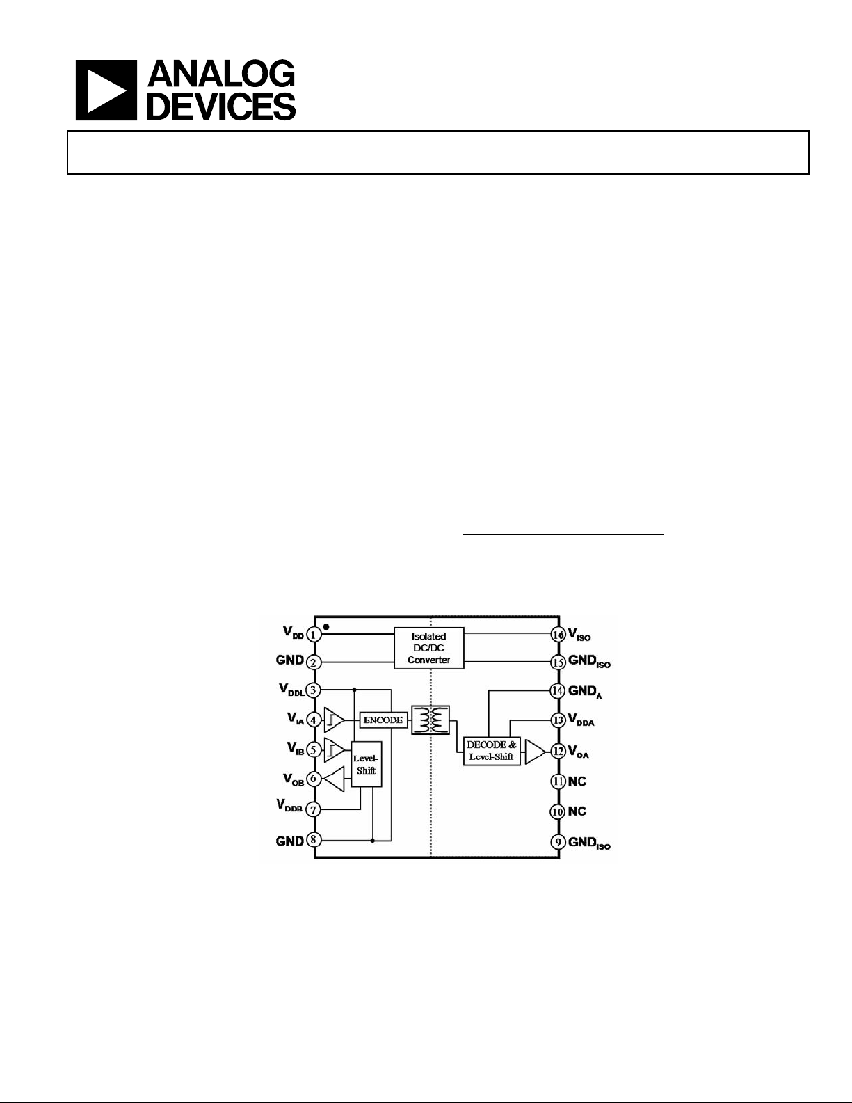
FUNCTIONAL BLOCK DIAGRAM
ADuM6132
GENERAL DESCRIPTION
The ADuM61321 is an isolated half-bridge gate driver that employs
Analog Devices’ iCoupler® technology to provide an isolated highside driver with an integrated 300 mW high-side supply. This
supply, provided by an internal isolated DC/DC converter powers
not only the ADuM6132’s high-side output but also any external
buffer circuitry that would commonly be used with the
ADuM6132.
difficulties associated with external supply configurations such
as a bootstrap circuitry.
channel and high side power from the control and low side
interface circuitry. Care has been taken to ensure close matching
between the high and low side driver timing characteristics,
reduces the need for dead time margin.
In comparison to gate drivers employing high voltage level
translation methodologies, the ADuM6132 offers the benefit of
true, galvanic isolation. The differential voltage between high and
low side channels can be as high as 1131V in some configurations
(see Table 7).
1
Protected by U.S. Patents 5,952,849; 6,873,065; and 7,075 329. Other patents
pending.
This eliminates the cost, space, and performance
The architecture isolates the high side
Figure 1. ADuM6132 Functional Block Diagram
Rev. PrG March 19, 2008
Information furnished by Analog Devices is believed to be accurate and reliable.
However, no responsibility is assumed by Analog Devices for its use, nor for any
infringements of patents or other rights of third parties that may result from its use.
Specifications subject to change without notice. No license is granted by implication
or otherwise under any patent or patent rights of Anal og Devices. Trademarks and
registered trademarks are the property of their respective owners.
One Technology Way, P.O. Box 9106, Norwood, MA 02062-9106, U.S.A.
Tel: 781.329.4700 www.analog.com
Fax: 781.326.8703 © 2008 Analog Devices, Inc. All rights reserved.
Page 2
ADuM6132 PRELIMINARY TECHNICAL DATA
SPECIFICATIONS
ELECTRICAL CHARACTERISTICS
All voltages are relative to their respective ground. 4.5 ≤ VDD = V
apply over the entire recommended operating range, unless otherwise noted. All typical specifications are at T
5.0V, V
= 15 V, V
DDB
DDA
= V
ISO
.
Table 1.
Parameter Symbol Min Typ Max Unit Test Conditions
DC SPECIFICATIONS
Isolated Power Supply
Input Current, Quiescent
I
DD
(Q)
Input Current, Loaded IDD 350 mA I
Maximum Output Current1 I
Output Voltage V
22 mA 12.5 < V
ISO(max)
12.5 15 17 V 0 < I
ISO
Logic Supply
Input Current I
1.8 3.0 mA
DDL
Output Supplies, Channel A or Channel B2
Supply Current, Quiescent
Supply Current, fIN=20kHz
Supply Current, fIN=100kHz
Supply Current, fIN=1000kHz
I
DDA
(Q)
I
DDA(20)
I
DDA(100)
I
DDA(1000)
, I
,
DDB
I
DDB(20)
I
DDB(100)
,
I
DDB(1000)
,
(Q)
Logic Inputs, Channel A or Channel B
Input Current IIA, I
Logic High Input Voltage V
Logic Low Input Voltage V
IB
, V
0.7 xV
IAH
IBH
, V
IAL
IBL
Outputs, Channel A or Channel B
Channel A High Level Output Voltage V
Channel B High Level Output Voltage V
Low Level Output Voltages V
High Level Output Current, Peak3 I
Low Level Output Current, Peak3 I
Undervoltage Lockout, V
DDA
or V
Supply
DDB
Positive going threshold V
Negative going threshold V
Hysteresis V
Undervoltage Lockout, V
Supply
DDL
Positive going threshold V
Negative going threshold V
Hysteresis V
V
OAH
V
OBH
0.1 V I
OAL,VOBL
, I
200 mA
OAH
OBH
, I
200 mA
OAL
OBL
DDAUV+, VDDBUV+
DDAUV-, VDDBUV-
, V
DDBUVH
DDBUVH
DDLUV+
DDLUV-
DDLUVH
SWITCHING SPECIFICATIONS
Minimum Pulse Width4 PW 50 ns CL = 200 pF
Maximum Switching Frequency5 f
Propagation Delay
6
1000 KHz CL = 200 pF
IN
t
, t
40 60 100 ns CL = 200 pF
PHL
PLH
Change versus temperature 100
Pulse-Width Distortion, |t
Channel-to-Channel Matching, Rising or
Falling Matching Edge Polarity
Channel-to-Channel Matching, Rising vs.
Falling Opposite Edge Polarity
| PWD 10 ns CL = 200 pF
PLH−tPHL
t
20 ns CL = 200 pF
7
8
M2
20 ns CL = 200 pF
t
M1
Part-to-Part Matching9 60 ns CL = 200 pF
Output Rise Time (10%−90%) tR 15 ns CL = 200 pF
Output Fall Time (10%−90%) tF 15 ns CL = 200 pF
≤ 5.5 V, 12.5 ≤ V
DDL
≤ 17.0 V, V
DDB
250 mA I
DDA
= V
. All min/max specifications
ISO
= 25°C, VDD = V
A
=0, DC signal inputs
ISO
= I
ISO
ISO(max,)
ISO
< 22
ISO
DDL
< 17.0
1.0 2 mA
1.1 2.1 mA CL = 200 pF
1.3 2.3 mA CL = 200 pF
4.5 5.5 mA CL = 200 pF
−10 0.01 10 μA 0 ≤ VIA, VIB ≤ 5.5V
DDL
–0.1
DDA
–0.1 V I
DDB
0.3 x V
V I
V
V
DDL
= -1 mA
OAH
= -1 mA
OBH
, I
OAL
= +1 mA
OBL
11.0 11.7 12.3 V
10.0 10.7 11.2 V
0.8 1.0 1.2 V
3.5 4.2 V
3.0 3.7 V
0.3 V
ps/°
C
=
Rev. PrG| Page 2 of 12
Page 3

PRELIMINARY TECHNICAL DATA
ADuM6132
1
The maximum output current is the maximum isolated supply current that the ADuM6132 can provide. This current supports external loads as well as the needs of
the ADuM6132 Channel A output circuitry. This is achieved via external connection of V
external loads is the ADuM6132 output current I
2
I
is supplied by the output of the integrated isolated dc/dc power as described in Footnote 1 above. I
DDA
Figure 3.
3
Duration less than 1 second. Average output current must conform to the limit shown under the Absolute Maximum Ratings.
4
The minimum pulse width is the shortest pulse width at which the specified pulse width distortion is guaranteed. Operation below the minimum pulse width is not
recommended.
5
The maximum switching frequency is the maximum signal frequency at which the specified timing parameters are guaranteed. Operation beyond the maximum
frequency is not recommended since high switching rates can cause droop in the output supply voltage.
6
t
propagation delay is measured from the 50% level of the falling edge of the VIx signal to the 50% level of the falling edge of the VOx signal. t
PHL
measured from the 50% level of the rising edge of the VIx signal to the 50% level of the rising edge of the VOx signal.
7
“Channel-to-channel matching, rising or falling matching edge polarity” is the magnitude of the propagation delay difference between two channels of the same part
when both inputs are either both rising or falling edges. The loads on each channel are equal.
8
“Channel-to-channel matching, rising vs. falling opposite edge polarity” is the magnitude of the propagation delay difference between two channels of the same part
when one input is a rising edge and one input is a falling edge. The loads on each channel are equal.
9
Part-to-part matching is the magnitude of the propagation delay difference between the same channels of two different parts. This includes rising vs. rising, falling vs.
falling, or rising vs. falling edges. The supply voltages, temperatures, and loads of each part are equal.
less the Channel A supply current I
ISO
DDA
to V
and GND
ISO
DDA
.
to GNDA (Figure 3). The net current available to power
ISO
is supplied by external power connection to V
DDB
propagation delay is
PLH
pin. See
DDB
Rev. PrG| Page 3 of 12
Page 4
ADuM6132 PRELIMINARY TECHNICAL DATA
PACKAGE CHARACTERISTICS
Table 2.
Parameter Symbol Min Typ Max Unit Test Conditions
Resistance (Input Side- High Side Output)1 R
Capacitance (Input to High Side Output)1 C
Input Capacitance CI 4.0 pF
IC Junction-to-Ambient Thermal Resistance θJA 45 °C/W 4-layer PC board
1
The device is considered a two-terminal device: Pins 1-8 are shorted together, and Pins 9-16 are shorted together.
REGULATORY INFORMATION
The ADuM6132 will be approved by the organizations listed in Table 3.
Table 3.
UL (pending) CSA (Pending) VDE (Pending)
Recognized under 1577
component recognition program
Double/reinforced insulation,
3750 V rms isolation voltage
Approved under CSA Component
1
Acceptance Notice #5A
Basic insulation per CSA 60950-1-03 and IEC
60950-1, 800 V rms (1131 V peak) maximum
working voltage
Reinforced insulation per CSA 60950-1-03 and
IEC 60950-1, 400 V rms maximum working voltage
File E214100 File 205078 File 2471900-4880-0001
1
In accordance with UL1577, each ADuM6132 is proof tested by applying an insulation test voltage ≥ 4500 V rms for 1 second (current leakage detection limit = 10 μA).
2
In accordance with DIN V VDE V 0884-10, each ADuM6132 is proof tested by applying an insulation test voltage ≥1050 V peak for 1 sec (partial discharge detection
limit = 5 pC). The * marking branded on the component designates DIN V VDE V 0884-10 approval.
INSULATION AND SAFETY-RELATED SPECIFICATIONS
Table 4.
Parameter Symbol Value Unit Conditions
Rated Dielectric Insulation Voltage 3750 V rms 1 minute duration
Minimum External Air Gap (Clearance) L(I01) 8.0 min mm Measured from input terminals to output terminals, shortest
Minimum External Tracking (Creepage) L(I02) 8.0 min mm
Minimum Internal Gap (Internal
Clearance)
Tracking Resistance (Comparative
Tracking Index)
Isolation Group IIIa Material Group (DIN VDE 0110, 1/89, Table 1)
0.017 min mm Insulation distance through insulation
CTI >175 V DIN IEC 112/VDE 0303 Part 1
1012 Ω
I-O
2.0 pF
I-O
Certified according to DIN V VDE V 0884-10
(VDE V 0884-10):2006-122
Reinforced insulation, 560 V peak
Complies with DIN EN 60747-5-2 (VDE 0884
Part 2): 2003-01, DIN EN 60950 (VDE 0805):
2001-12; EN 60950: 2000, DIN V VDE 0884-10
(VDE V 0884-10):2006-12
distance through air
Measured from input terminals to output terminals, shortest
distance path along body
Rev. PrG| Page 4 of 12
Page 5

PRELIMINARY TECHNICAL DATA
ADuM6132
DIN V VDE V 0884-10 (VDE V 0884-10) INSULATION CHARACTERISTICS
The ADuM6132 is suitable for reinforced electrical isolation only within the safety limit data. Maintenance of the safety data is ensured by
protective circuits. The * marking on the package denotes DIN V VDE V 0884-10 approval.
Table 5.
Description Conditions Symbol Characteristic Unit
Installation Classification per DIN VDE 0110
For Rated Mains Voltage ≤ 150 V rms I to IV
For Rated Mains Voltage ≤ 300 V rms I to III
For Rated Mains Voltage ≤ 400 V rms I to II
Climatic Classification 40/105/21
Pollution Degree (DIN VDE 0110, Table 1) 2
Maximum Working Insulation Voltage V
Input-to-Output Test Voltage, Method B1
× 1.875 = VPR, 100% production test, tm = 1 sec,
V
IORM
partial discharge < 5 pC
Input-to-Output Test Voltage, Method A V
× 1.6 = VPR, tm = 60 sec, partial discharge < 5 pC VPR
IORM
After Environmental Tests Subgroup 1 896 V peak
V
After Input and/or Safety Test Subgroup 2
× 1.2 = VPR, tm = 60 sec, partial discharge < 5 pC 672 V peak
IORM
and Subgroup 3
Highest Allowable Overvoltage Transient overvoltage, tTR = 10 sec VTR 6000 V peak
Safety-Limiting Values
Maximum value allowed in the event of a failure;
see
Case Temperature TS 150 °C
Side 1 Current IS1 265 mA
Side 2 Current IS2 335 mA
Insulation Resistance at TS VIO = 500 V RS >109 Ω
560 V peak
IORM
1050 V peak
V
PR
RECOMMENDED OPERATING CONDITIONS
Table 6.
Parameter Symbol Min Max Unit
Operating Temperature TA −40 +105 °C
Input Supply Voltage1 V
Channel B Supply Voltage1 V
Input Signal Rise and Fall Times 1 ms
Common-Mode Transient Immunity, Input-to-Output −50 +50 kV/μs
1
All voltages are relative to their respective ground.
4.5 5.5 V
DD
12.5 17 V
DDB
Rev. PrG| Page 5 of 12
Page 6

ADuM6132 PRELIMINARY TECHNICAL DATA
ABSOLUTE MAXIMUM RATINGS
Table 6.
Parameter Symbol Min Max Unit
Storage Temperature TST −55 +150 °C
−40 +105 °C
Ambient Operating
T
A
Temperature
Input Supply Voltage1 VDD −0.5 +7.0 V
−0.5 +27 V
Channel B Supply
1
Voltage
Input Voltage1 V
Output Voltage1 V
Output DC Current IOA, I
Common-Mode
Transients
2
V
DDB
, VIB −0.5 V
IA
, VOB −0.5
OA
OB
−100 +100 mA
+ 0.5 V
DDI
+ 0.5,
V
ISO
V
+ 0.5
DDB
V
−100 +100 kV/μs
1
All voltages are relative to their respective ground.
2
Refers to common-mode transients across any insulation barrier. Common-
mode transients exceeding the Absolute Maximum Ratings can cause latchup or permanent damage.
Stresses above those listed under Absolute Maximum Ratings
may cause permanent damage to the device. This is a stress
rating only; functional operation of the device at these or any
other conditions above those listed in the operational sections
of this specification is not implied. Exposure to absolute
maximum rating conditions for extended periods may affect
device reliability.
Ambient temperature = 25°C, unless otherwise noted.
ESD CAUTION
Table 7. Maximum Continuous Working Voltage
1
Parameter Max Unit Constraint
AC Voltage, Bipolar Waveform 565 V peak
AC Voltage, Unipolar Waveform V peak
Basic Insulation 1131 V peak
50-year minimum lifetime
Maximum approved working voltage per IEC 60950-1
DC Voltage
Basic Insulation 1131 V peak
1
Refers to continuous voltage magnitude imposed across the isolation barrier. See the Insulation Lifetime section for more details
600
500
400
300
200
100
Sa fe Operating VDD1 Current (mA)
0
0 50 100 150 200
Amb ien t Tempearture ( °C)
Maximum approved working voltage per IEC 60950-1
Figure 2 Thermal Derating Curve, Dependence of Safety Limiting Values on
Case Temperature, per DIN EN 60747-5-2
Rev. PrG| Page 6 of 12
Page 7

PRELIMINARY TECHNICAL DATA
PIN CONFIGURATIONS AND PIN FUNCTION DESCRIPTIONS
Figure 3. ADuM6132 Pin Configuration
Table 8. ADuM6132 Pin Function Descriptions
Pin
No. Mnemonic Function
1 V
2 GND
3 V
4 V
5 V
6 V
7 V
DD
Input supply voltage for logic, 4.5V to 5.5V
DDL
IA
IB
OB
DDB
8 GND Ground reference for isolated power supply input and logic inputs
9 GND
Ground reference for isolated power supply output
ISO
10 NC No Connect
11 NC No Connect
12 VOA Output A (isolated)
13 V
Output A supply voltage input, must be connected externally to V
DDA
14 GNDA Output A ground reference, must be connected externally to GND
15 GND
16 V
ISO
Isolated power supply voltage output
ISO
Table 9. ADuM6132 Truth Table (Positive Logic)
VIA
Input
VIB
Input
V
State V
DDL
L L Powered Powered L L
L H Powered Powered L H
H L Powered Powered H L
H H Powered Powered H H
X X Unpowered Powered L L
X X Powered Unpowered L L
Input supply voltage for isolated power supply, 4.5V to 5.5V
Ground reference for isolated power supply input and logic inputs
Logic input A
Logic input B
Output B (non-isolated).
Output B supply voltage input (non-isolated),
12.5V to 17V
Ground reference for isolated power supply output
State VOA
DDB
Output
VOB
Output
Notes
returns to input state within 1 μs
V
OA
power restoration.
of V
DD
ISO
(pin 15)
ISO
ADuM6132
(pin16)
Rev. PrG| Page 7 of 12
Page 8

ADuM6132 PRELIMINARY TECHNICAL DATA
APPLICATION INFORMATION
TYPICAL APPLICATION USAGE
The architecture of the ADuM6132 is ideal for motor drive and
inverter applications where the low side channels are common
to the controller. This arrangement requires only two isolation
regions in a package. All of the isolated signals and Isolated
power are grouped on one side of the package so full package
creepage and clearance are maintained. The low side drive as
well as the control signals share a common reference and are
also grouped together.
In order to maximize the efficacy of external bypass capacitors,
the isoPower DC/DC converter is not internally tied to the data
channels, and should be treated as a completely independent
subsystem, except for a UVLO function (see Undervoltage
lockout). This means that power must be applied to V
operate the DC/DC converter. Power must also be applied to
V
DDL
and V
to operate the data input and the channel B
DDB
driver output. On the secondary side, the power generated at
the VISO pin must be applied as an input power supply to the
V
pin. GND
DDA
and GNDA must be connected together.
ISO
The ADuM6132 is intended for driving low gate capacitance
transistors (200 pF typically). Most high voltage applications
involve larger transistors than this. To accommodate these
applications, users can implement a buffer configuration with
the ADuM6132 as shown in Figure 3. In many cases, this buffer
configuration is the least expensive option to drive high
capacitance devices and provides the greatest amount of design
flexibility. The precise buffer/high voltage transistor
combination can be selected to fit the needs of the application.
DD
to
Figure 3. Typical Application Circuit
PC BOARD LAYOUT
The ADuM6132 digital isolator with integrated 250mW
isoPower DC/DC converter requires no external interface
circuitry for the logic interfaces. Power supply bypassing is
required at the input and output supply pins (Figure 4). The
power supply section of the ADuM6132 uses a very high
oscillator frequency to efficiently pass power through its chip
scale transformers. In addition, the normal operation of the
data section of the iCoupler introduces switching transients on
the power supply pins. Bypass capacitors are required for
several operating frequencies. Noise suppression requires a low
ESR high frequency capacitor, ripple suppression and proper
regulation require a large value capacitor in parallel, see Table
10. The total lead length between both ends of the capacitor and
the input power supply pin should not exceed 20 mm.
Supply Pins Bypass Capacitors
VDD 1,2 0.1μF, 10μF
V
7,8 0.1μF
DDB
V
2,3 0.1μF
DDL
V
13,14 0.1μF
DDA
V
15,16 0.1μF, 10μF
ISO
Table 10 Recommended Bypass Capacitors
In applications involving high common-mode transients, care
should be taken to ensure that board capacitive coupling across the
isolation barrier is minimized. Furthermore, the board layout
should be designed such that any coupling that does occur
equally affects all pins on a given component side. Failure to
ensure this could cause voltage differentials between pins
exceeding the device’s Absolute Maximum Ratings, specified in
Error! Reference source not found. leading to latch-up and/or
permanent damage.
The ADuM6132 is a power device that dissipates about 1W of
power when fully loaded and running at maximum speed.
Since it is not possible to apply a heat sink to an isolation
device, the device primarily depends on heat dissipation into
the PCB through the GND pins. If the device will be used at
high ambient temperatures, care should be taken to provide a
Rev. PrG| Page 8 of 12
thermal path from the GND pins to the PCB ground plane.
Figure 4. Recommended Printed Circuit Board Layout
Page 9

PRELIMINARY TECHNICAL DATA
V
The board layout in Figure 4 shows enlarged pads for pins 8 and
9. Multiple vias should be implemented from the pad to the
ground plane. This will significantly reduce the temperatures
inside of the chip. The dimensions of the expanded pads are
left to discretion of the designer and the available board space.
THERMAL ANALYSIS
The ADuM6132 parts consist of several internal die, attached to
two lead frame paddles. For the purposes of thermal analysis it
is treated as a thermal unit with the highest junction
temperature reflected in the θ
not found. The value of θ
from Error! Reference source
JA
is based on measurements taken
JA
with the part mounted on a JEDEC standard 4 layer board with
fine width traces and still air. Under normal operating
conditions the ADuM6132 will operate at full load across the
full temperature range without derating the output current.
However, following the recommendations in the PC Board
Layout section will decrease the thermal resistance to the PCB
allowing increased thermal margin it high ambient
temperatures.
UNDERVOLTAGE LOCKOUT
The ADuM6132 has undervoltage lockout (UVLO) circuits on
, V
the V
DDL
DDA
, and V
UVLO circuit monitors the supply voltage and takes a
predetermined action based on whether the supply voltage is
above or below a given threshold. These thresholds are
specified in Table 1.
In the recommended configuration of Figure 3 only two
independent supplies are controlled by the user: V
V
DDL/VDD
(V
DDL=VDD
internal DC/DC converter via the V
connection. Nevertheless, the V
included in the below table so that the user has an
understanding of the V
DC/DC converter powers on and off.
supplies. For each supply its respective
DDB
and
DDB
in Figure 3). V
output behavior as the internal
OA
is supplied by the
DDA
ISO=VDDA
UVLO functionality is
DDA
external
ADuM6132
Table 11. Undervoltage Lockout Functionality Table
-
V
User-provided
supplies
V
DDL
Supply
V
DDB
Supply
H H H
H H L
X L X
L X X
Notes:
L: denotes supply voltage < undervoltage lockout threshold
H: denotes supply voltage > undervoltage lockout threshold
X: denotes supply voltage level is irrelevant
When all three supplies are above their respective UVLO
thresholds the ADuM6132 operates normally. The internal
DC/DC converter is active and both outputs operate as
determined by their respective input logic signals. If either of
the user-provided supplies is below its UVLO threshold, the
ADuM6132 is put into a disabled mode. In this mode the
internal DC/DC converter is turned off and both outputs are
driven low. The V
V
UVLO circuit (whichever is below its threshold). The VOA
DDB
output is driven low as the internal DC/DC converter is turned
off. The V
connected to V
supply voltage is drops to zero. Since V
ISO
ISO
below its UVLO threshold V
circuit.
ISO
powered
supply
V
DDA
Supply
Resultant
Effect
Normal operation.
Internal DC/DC converter active.
output logic states
V
OA/VOB
match V
input logic states.
IA/VIB
Internal DC/DC converter active
but V
belpow UVLO threshold.
ISO
output driven low.
V
OA
V
output operates normally.
OB
Internal DC/DC converter turned
off (V
= 0).
ISO
output driven low.
V
OA
V
output drive low.
OB
Internal DC/DC converter turned
off (V
= 0).
ISO
output driven low.
V
OA
V
output drive low.
OB
output is driven low by either the V
OB
is
DDA
, it also is brought down to zero. Once V
is driven low by the V
OA
DDA
UVLO
DDL
or
DDA
is
PROPAGATION DELAY-RELATED PARAMETERS
Propagation delay is a parameter that describes the time it takes
a logic signal to propagate through a component. The propagation
delay to a logic low output may differ from the propagation
delay to a logic high.
INPUT (
OUTPUT (V
Pulse width distortion is the maximum difference between
these two propagation delay values and is an indication of how
Rev. PrG| Page 9 of 12
)
IX
t
PLH
)
OX
Figure 5. Propagation Delay Parameters
t
PHL
50%
50%
03786-018
Page 10

ADuM6132 PRELIMINARY TECHNICAL DATA
accurately the input signal’s timing is preserved.
Channel-to-channel matching refers to the maximum amount
the propagation delay differs between channels within a single
ADuM6132 component.
MAGNETIC FIELD IMMUNITY
The ADuM6132 is extremely immune to external magnetic
fields. The limitation on the ADuM6132’s magnetic field
immunity is set by the condition in which induced voltage in
the transformer’s receiving coil is sufficiently large to either
falsely set or reset the decoder. The following analysis defines
the conditions under which this may occur.
The pulses at the transformer output have an amplitude greater
than 1.0 V. The decoder has a sensing threshold at about 0.5 V, thus
establishing a 0.5 V margin in which induced voltages can be
tolerated. The voltage induced across the receiving coil is given by
2
=Π−= NnrdtdV
...,2,1;)/β(
1M
100M100k
06401-010
∑
n
where:
β is the magnetic flux density (gauss).
N is the number of turns in the receiving coil.
r
is the radius of the nth turn in the receiving coil (cm).
n
Given the geometry of the receiving coil in the ADuM6132 and
an imposed requirement that the induced voltage is at most
50% of the 0.5 V margin at the decoder, a maximum allowable
magnetic field is calculated, as shown in Figure 6.
100
10
1
0.1
DENSITY (kgauss)
0.01
MAXIMUM ALLOWABLE MAGNETIC FLUX
0.001
1k 10k 10M
Figure 6. Maximum Allowable External Magnetic Flux Density
MAGNETIC F IELD FREQ UE NCY (Hz)
For example, at a magnetic field frequency of 1 MHz, the
maximum allowable magnetic field of 0.2 kgauss induces a
voltage of 0.25 V at the receiving coil. This is about 50% of the
sensing threshold and does not cause a faulty output transition.
Similarly, if such an event occurs during a transmitted pulse
(with the worst-case polarity), it reduces the received pulse
from > 1.0 V to 0.75 V. Note that this is still well above the 0.5 V
sensing threshold of the decoder.
The preceding magnetic flux density values correspond to
specific current magnitudes at given distances away from the
ADuM6132 transformers. Figure 7 expresses these allowable
current magnitudes as a function of frequency for selected
distances. As shown in Figure 7, the ADuM6132 is extremely
immune and can be affected only by extremely large currents
operated at high frequency and very close to the component.
For the 1 MHz example, one would have to place a 0.5 kA
current 5 mm away from the ADuM6132 to affect the
component’s operation.
1000
DISTANCE = 1m
100
10
DISTANCE = 100mm
1
DISTANCE = 5mm
0.1
MAXIMUM ALLOWABLE CURRENT (kA)
0.01
1k 10k 100M100k 1M 10M
MAGNETIC F I ELD FREQUENCY (Hz)
Figure 7. Maximum Allowable Current for Various
Current-to-ADuM6132 Spacings
06401-011
Note that at combinations of strong magnetic fields and high
frequencies, any loops formed by printed circuit board traces
could induce sufficiently large error voltages to trigger the
threshold of succeeding circuitry. Care should be taken in the
layout of such traces to avoid this possibility.
INSULATION LIFETIME
All insulation structures eventually break down when subjected
to voltage stress over a sufficiently long period. The rate of
insulation degradation depends on the characteristics of the
voltage waveform applied across the insulation. In addition to
the testing performed by the regulatory agencies, Analog
Devices conducts an extensive set of evaluations to determine
the lifetime of the insulation structure within the ADuM5230.
Analog Devices performs accelerated life testing using voltage
levels higher than the rated continuous working voltage.
Acceleration factors for several operating conditions are
determined. These factors allow calculation of the time to
failure at the actual working voltage. Table 7 summarizes the
peak voltages for 50 years of service life for a bipolar ac
operating condition and the maximum Analog Devices
recommended working voltages. In many cases, the approved
working voltage is higher than the 50-year service life voltage.
Operation at these high working voltages can lead to shortened
insulation life in some cases.
The insulation lifetime of the ADuM6132 depends on the
Rev. PrG| Page 10 of 12
Page 11

PRELIMINARY TECHNICAL DATA
voltage waveform type imposed across the isolation barrier.
The iCoupler insulation structure degrades at different rates
depending on whether the waveform is bipolar ac, unipolar ac,
or dc. Figure 8, Figure 9, and Figure 10 illustrate these different
isolation voltage waveforms.
Bipolar ac voltage is the most stringent environment. The goal
of a 50-year operating lifetime under the ac bipolar condition
determines the maximum working voltage recommended by
Analog Devices.
In the case of unipolar ac or dc voltage, the stress on the insulation is significantly lower. This allows operation at higher
working voltages while still achieving a 50-year service life.
The working voltages listed in Table 7 can be applied while
maintaining the 50-year minimum lifetime provided the voltage
conforms to either the unipolar ac or dc voltage cases. Any cross
insulation voltage waveform that does not conform to Figure 9
or Figure 10 should be treated as a bipolar ac waveform and its
peak voltage should be limited to the 50-year lifetime voltage
value listed in Table 7. Note that the voltage presented in Figure 9 is
shown as sinusoidal for illustration purposes only. It is meant to
represent any voltage waveform varying between 0 V and some
limiting value. The limiting value can be positive or negative,
but the voltage cannot cross 0 V.
ADuM6132
RATED PEAK VOLTAGE
0V
Figure 8. Bipolar AC Waveform
RATED PEAK VOLTAGE
0V
Figure 9. Unipolar AC Waveform
RATED PEAK VOLTAGE
0V
Figure 10. DC Waveform
06920-014
06920-015
06920-016
Rev. PrG| Page 11 of 12
Page 12

ADuM6132 PRELIMINARY TECHNICAL DATA
OUTLINE DIMENSIONS
10.50 (0.4134)
10.10 (0.3976)
16
1
1.27 (0.0500)
BSC
0.30 (0.0118)
0.10 (0.0039)
COPLANARITY
0.10
CONTROLLING DIMENSIONS ARE IN MILLIMETERS; INCH DIMENSIONS
(IN PARENTHESES) ARE ROUNDED-OFF MILLIMETER EQUIVALENTS FOR
REFERENCE ONLY AND ARE NOT APPROPRIATE FOR USE IN DESIGN
0.51 (0.0201)
0.31 (0.0122)
COMPLIANT TO JEDEC STANDARDS MS-013AA
9
7.60 (0.2992)
7.40 (0.2913)
8
2.65 (0.1043)
2.35 (0.0925)
SEATING
PLANE
10.65 (0.4193)
10.00 (0.3937)
0.33 (0.0130)
0.20 (0.0079)
0.75 (0.0295)
0.25 (0.0098)
8°
0°
× 45°
1.27 (0.0500)
0.40 (0.0157)
Figure 6. 16-Lead Standard Small Outline Package [SOIC]— Wide Body (RW-16).
Dimensions shown in millimeters (inches)
ORDERING GUIDE
No. of
Model
Channels
ADuM6132ARWZ1 2 0.2 15 −40°C to +105°C 16-Lead SOIC_W RW-16
ADuM6132ARWZ-RL1 2 0.2 15 −40°C to +105°C
1
Z = Pb-free part.
Output Peak
Current (A)
Output
Voltage (V)
Temperature Range Package Description
16-Lead SOIC_W, 13-inch Tape
and Reel Option (1, 000 Units)
Package
Option
RW-16
©2008 Analog Devices, Inc. All rights reserved. Trademarks and
registered trademarks are the property of their respective owners.
PR07393-0-3/08(PrG)
Rev. PrG| Page 12 of 12
 Loading...